FEARURES
DESCRIPTION
Internal LDO Regulator
12V High Voltage Supply
300MHz to 450MHz Frequency Range
Data Rates up to 10kbps ASK
Output Power to 17dBm on 50ohm load
Low external part count
SOT23-6 Package Type
Applications
Fan Controllers
Remote Power Switches
Multi-Media Remote Control
Remote Sensor Data Links
Infrared Transmitter Replacement
The F115H is a high voltage supply, high performance,
internal 3V LDO regulator output, single chip ASK
transmitter IC for remoter wireless applications in the
300 to 450MHz frequency band.
This transmitter IC is a true “data-in, antenna-out”
monolithic device, in terms of power, the F115H is
capable of delivering 17dBm into a 50ohm load
(matched). In the terms of operating voltage, the
F115H operates from 5V to 14V. In the terms of
internal LDO regulator, the regulator can output 3V
voltage supply for encode ICs or MCU, and up to
60mA load current with external 1uF capacitor when
12V input Voltage.
The F115H is easy to use, it requires a reference
frequency (RF carrier frequency divide by 32 times)
generated from a crystal without external capacitor. No
external matching network components
for PCB
antenna application.
The F115H operates with ASK/OOK UHF receiver
types from wide-band super-regenerative radios to
narrow-band, high performance super-heterodyne
receivers. The F115H’s maximum ASK data rate is
10kbps. The ASK data voltage should be under 3.6V.
*This preliminary datasheet is subject to change without notification.
- 1 -
�
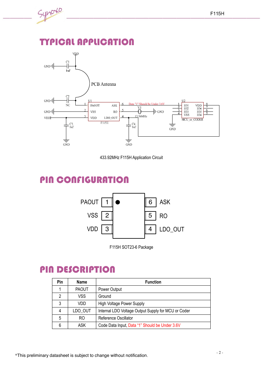
TYPICAL APPLICATION
433.92MHz F115H Application Circuit
PIN CONFIGURATION
F115H SOT23-6 Package
PIN DESCRIPTION
Pin
Name
Function
1
2
3
4
5
6
PAOUT
Power Output
VSS
VDD
Ground
High Voltage Power Supply
LDO_OUT
Internal LDO Voltage Output Supply for MCU or Coder
RO
ASK
Reference Oscillator
Code Data Input, Data “1” Should be Under 3.6V
*This preliminary datasheet is subject to change without notification.
- 2 -
ASKPAOUTVSSVDD1236RO5LDO_OUT4�
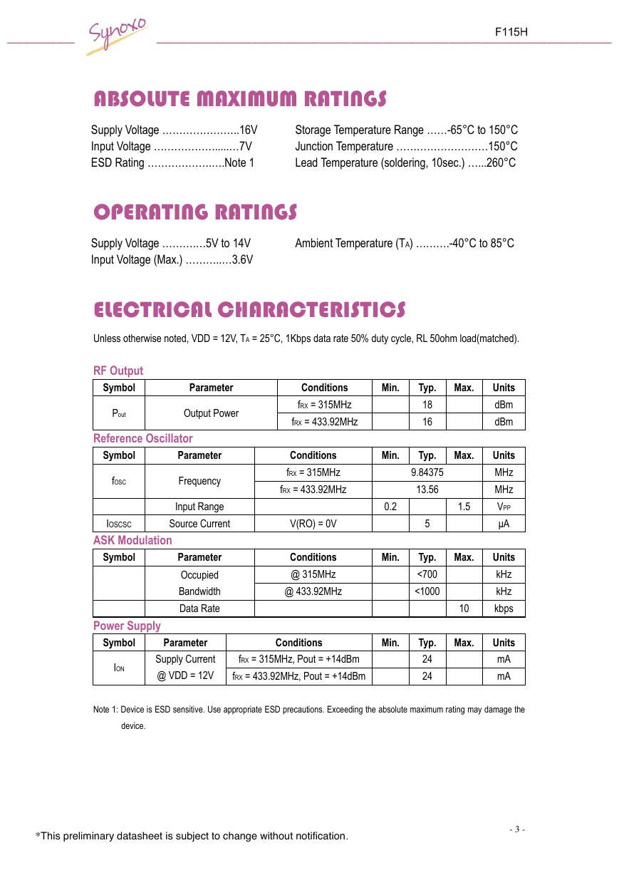
ABSOLUTE MAXIMUM RATINGS
Supply Voltage …………………..16V
Input Voltage ……………….....…7V
ESD Rating ……………….….Note 1
Storage Temperature Range ……-65° C to 150° C
Junction Temperature ………………………150° C
Lead Temperature (soldering, 10sec.) …...260° C
OPERATING RATINGS
Supply Voltage ……….…5V to 14V
Input Voltage (Max.) ………..…3.6V
Ambient Temperature (TA) ……….-40° C to 85° C
ELECTRICAL CHARACTERISTICS
Unless otherwise noted, VDD = 12V, TA = 25° C, 1Kbps data rate 50% duty cycle, RL 50ohm load(matched).
RF Output
Symbol
Parameter
Conditions
Min.
Typ.
Max.
Units
Pout
Output Power
Reference Oscillator
fRX = 315MHz
fRX = 433.92MHz
18
16
dBm
dBm
Symbol
Parameter
Conditions
Min.
Typ.
Max.
Units
fOSC
Frequency
Input Range
fRX = 315MHz
fRX = 433.92MHz
IOSCSC
Source Current
V(RO) = 0V
9.84375
13.56
0.2
5
1.5
MHz
MHz
VPP
μA
ASK Modulation
Symbol
Parameter
Occupied
Bandwidth
Data Rate
Power Supply
Conditions
@ 315MHz
@ 433.92MHz
Min.
Typ.
Max.
Units
<700
<1000
kHz
kHz
10
kbps
Symbol
Parameter
Conditions
Min.
Typ.
Max.
Units
Supply Current
fRX = 315MHz, Pout = +14dBm
@ VDD = 12V
fRX = 433.92MHz, Pout = +14dBm
24
24
mA
mA
ION
Note 1: Device is ESD sensitive. Use appropriate ESD precautions. Exceeding the absolute maximum rating may damage the
device.
*This preliminary datasheet is subject to change without notification.
- 3 -
�
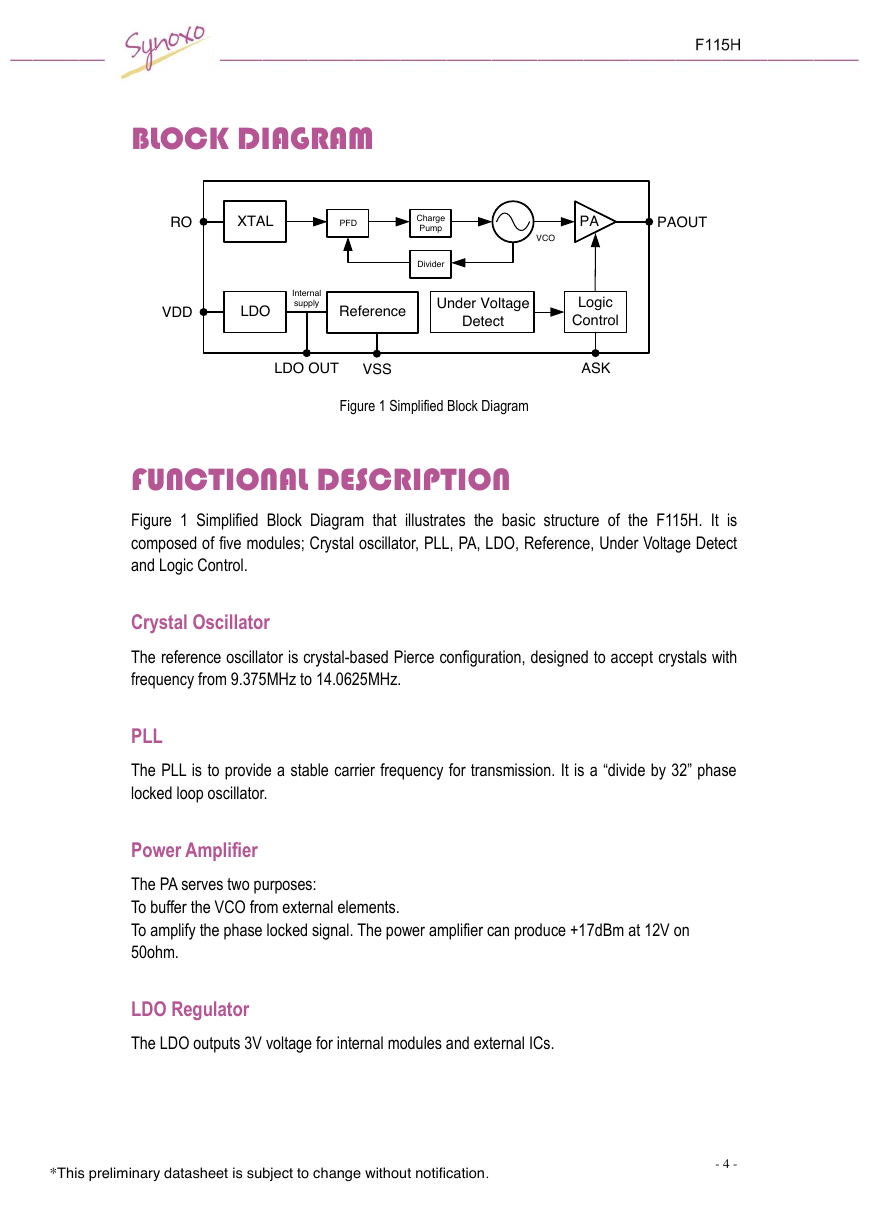
BLOCK DIAGRAM
Figure 1 Simplified Block Diagram
FUNCTIONAL DESCRIPTION
Figure 1 Simplified Block Diagram that illustrates the basic structure of the F115H. It is
composed of five modules; Crystal oscillator, PLL, PA, LDO, Reference, Under Voltage Detect
and Logic Control.
Crystal Oscillator
The reference oscillator is crystal-based Pierce configuration, designed to accept crystals with
frequency from 9.375MHz to 14.0625MHz.
PLL
The PLL is to provide a stable carrier frequency for transmission. It is a “divide by 32” phase
locked loop oscillator.
Power Amplifier
The PA serves two purposes:
To buffer the VCO from external elements.
To amplify the phase locked signal. The power amplifier can produce +17dBm at 12V on
50ohm.
LDO Regulator
The LDO outputs 3V voltage for internal modules and external ICs.
*This preliminary datasheet is subject to change without notification.
- 4 -
XTALPFDChargePumpDividerVCOPALDOLogic ControlUnder VoltageDetectROVDDVSSLDO OUTReferenceASKPAOUTInternal supply�
Reference
The reference provides the internal stable voltage and current
Under Voltage Detect
The block senses operating voltage. If the operating voltage falls below the setting voltage, this
block will send a signal to disable the PA.
Logic Control
The logic control gates the ASK data. It only allows transmission when lock, amplitude and
under voltage detect conditions are valid.
PCB LAYOUT
Layout Issues
For PCB antenna application, PCB layout is a primary concern for achieving optimum
performance and consistent manufacturing results, so PCB trace length should be short to
minimize parasitic inductance (25.4mm ~ 20nH), wide traces and a ground plane under the
signal traces is recommended.
Antenna Layout
No ground plane should be under the antenna trace, capacitance C2 normally don’t need.
Recommended for 433.92MHz application:
1. PCB antenna trace length is 45±5mm.
2. PCB antenna trace width is 1mm.
Recommended for 315MHz application:
1. PCB antenna trace length is 54±5mm.
2. PCB antenna trace width is 1mm.
*This preliminary datasheet is subject to change without notification.
- 5 -
�
PACKAGE DESCRIPTION
SOT23-6 Package Outline Dimensions shown in millimeters
*This preliminary datasheet is subject to change without notification.
- 6 -
�


 2023年江西萍乡中考道德与法治真题及答案.doc
 2012年重庆南川中考生物真题及答案.doc
 2013年江西师范大学地理学综合及文艺理论基础考研真题.doc
 2020年四川甘孜小升初语文真题及答案I卷.doc
 2020年注册岩土工程师专业基础考试真题及答案.doc
 2023-2024学年福建省厦门市九年级上学期数学月考试题及答案.doc
 2021-2022学年辽宁省沈阳市大东区九年级上学期语文期末试题及答案.doc
 2022-2023学年北京东城区初三第一学期物理期末试卷及答案.doc
 2018上半年江西教师资格初中地理学科知识与教学能力真题及答案.doc
 2012年河北国家公务员申论考试真题及答案-省级.doc
 2020-2021学年江苏省扬州市江都区邵樊片九年级上学期数学第一次质量检测试题及答案.doc
 2022下半年黑龙江教师资格证中学综合素质真题及答案.doc