I
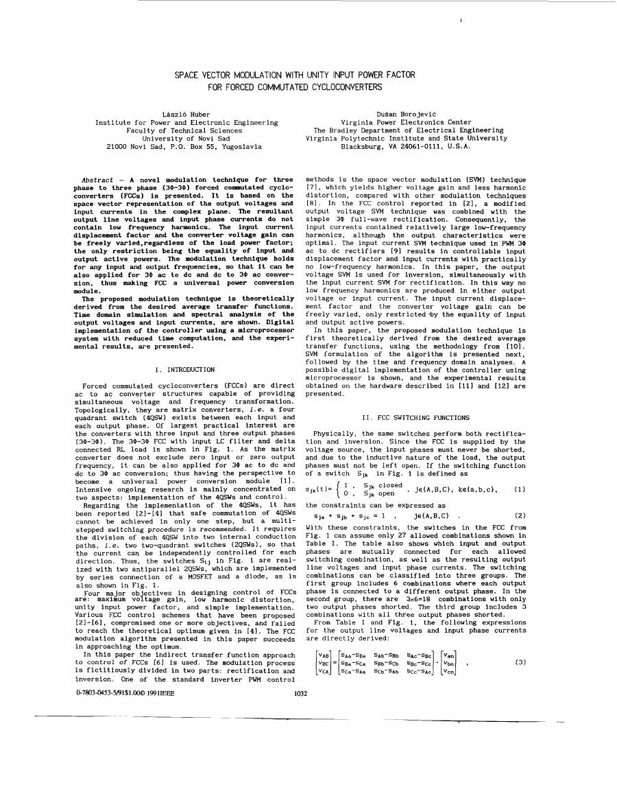
SPACE VECTOR MODULATION WITH UNITY INPUT POWER FACTOR
FOR FORCED COMMUTATED CYCLOCONVERTERS
Laszl6 Huber
Institute for Power and Electronic Engineering
Faculty of Technical Sciences
University of Novi Sad
21000 Novi Sad, P.O. Box 55, Yugoslavia
DuSan BorojeviC
Virginia Power Electronics Center
The Bradley Department of Electrical Engineering
Virginia Polytechnic Institute and State University
Blacksburg, VA 24061-0111, U.S.A.
Abstract - A novel modulation technique for three
phase to three phase (30-30) forced comnutated cyclo-
converters (FCCs) is presented. It is based on the
space vector representation of the output voltages and
input currents in the complex plane. The resultant
output line voltages and input phase currents do not
contain low frequency harmonics. The input current
displacement factor and the converter voltage gain can
be freely varied,regardless of the load power factor;
the only restriction being the equality of input and
output active powers. The modulation technique holds
for any input and output frequencies. so that it can be
also applied for 30 ac to dc and dc to 30 ac conver-
sion, thus making FCC a universal power conversion
module.
The proposed modulation technique is theoretically
derived from the desired average transfer functions.
Time domain simulation and spectral analysis of the
output voltages and input currents, are shown. Digital
implementation of the controller using a microprocessor
system with reduced time computation, and the experi-
mental results, are presented.
I . INTRODUCTION
Forced commutated cycloconverters (FCCs) are direct
ac to ac converter structures capable of providing
simultaneous voltage and frequency transformation.
Topologically, they are matrix converters, 1. e. a four
quadrant switch (4QSW) exists between each input and
each output phase. Of largest practical interest are
the converters with three input and three output phases
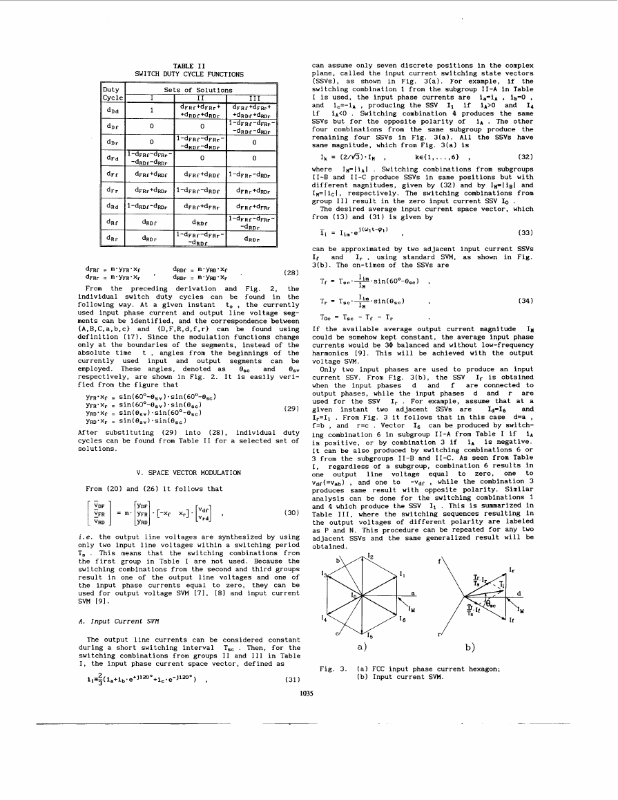
( 3 Q - 3 0 ) . The 30-30 FCC with input LC filter and delta
connected RL load is shown in Fig. 1. As the matrix
converter does not exclude zero input or zero output
frequency, it can be also applied for 30 ac to dc and
dc to 30 ac conversion; thus having the perspective to
become a universal power conversion module [11.
Intensive ongoing research is mainly concentrated on
two aspects: implementation of the 4QSWs and control.
Regarding the implementation of the 4QSWs. it has
been reported [21-[41 that safe commutation of 4QSWs
cannot be achieved in only one step, but a multi-
stepped switching procedure is recommended. It requires
the division of each 4QSW into two internal conduction
paths, i . e . two two-quadrant switches (ZQSWs), SO that
the current can be independently controlled for each
direction. Thus, the switches SlJ in Fig. 1 are real-
ized with two antiparallel ZQSWs, which are implemented
by series connection of a MOSFET and a diode, as is
also shown in Fig. 1.
Four major ob'ectives in designing control of FCCs
are: maximum voftage gain, low harmonic distortion,
unity input power factor, and simple implementation.
Various FCC control schemes that have been proposed
[21-[61, compromised one or more objectives, and failed
to reach the theoretical optimum given in [41. The FCC
modulation algorithm presented in this paper succeeds
in approaching the optimum.
In this paper the indirect transfer function approach
to control of FCCs [61 is used. The modulation process
is fictitiously divided in two parts: rectification and
inversion. One of the standard inverter PUM control
methods is the space vector modulation (SVM) technique
[71, which yields higher voltage gain and less harmonic
distortion, compared with other modulation techniques
[ S I . In the FCC control reported in [21, a modified
output voltage SVM technique was combined with the
simple 30 full-wave rectification. Consequently, the
input currents contained relatively large low-frequency
harmonics, although the output characteristics were
optimal. The input current SVM technique used in PWM 30
ac to dc rectifiers [91 results in controllable input
displacement factor and input currents with practically
no low-frequency harmonics. In this paper, the output
voltage SVM is used for inversion, simultaneously with
the input current SVM for rectification. In this way no
low frequency harmonics are produced in either output
voltage or input current. The input current displace-
ment factor and the converter voltage gain can be
freely varied, only restricted*by the equality of input
and output active powers.
In this paper, the proposed modulation technique is
first theoretically derived from the desired average
transfer functions, using the methodology from [lo].
SVM formulation of the algorithm is presented next,
followed by the time and frequency domain analyses. A
possible digital implementation of the controller using
microprocessor is shown, and the experimental results
obtained on the hardware described in [111 and [121 are
presented.
11. FCC SWITCHING FUNCTIONS
Physically, the same switches perform both rectifica-
tion and inversion. Since the FCC is supplied by the
voltage source, the input phases must never be shorted,
and due to the inductive nature of the load, the output
phases must not be left open. If the switching function
of a switch S j k in Fig. 1 is defined as
the constraints can be expressed as
jc{A,B,C} .
Sja + Sjb + Sjc = 1 ,
(2)
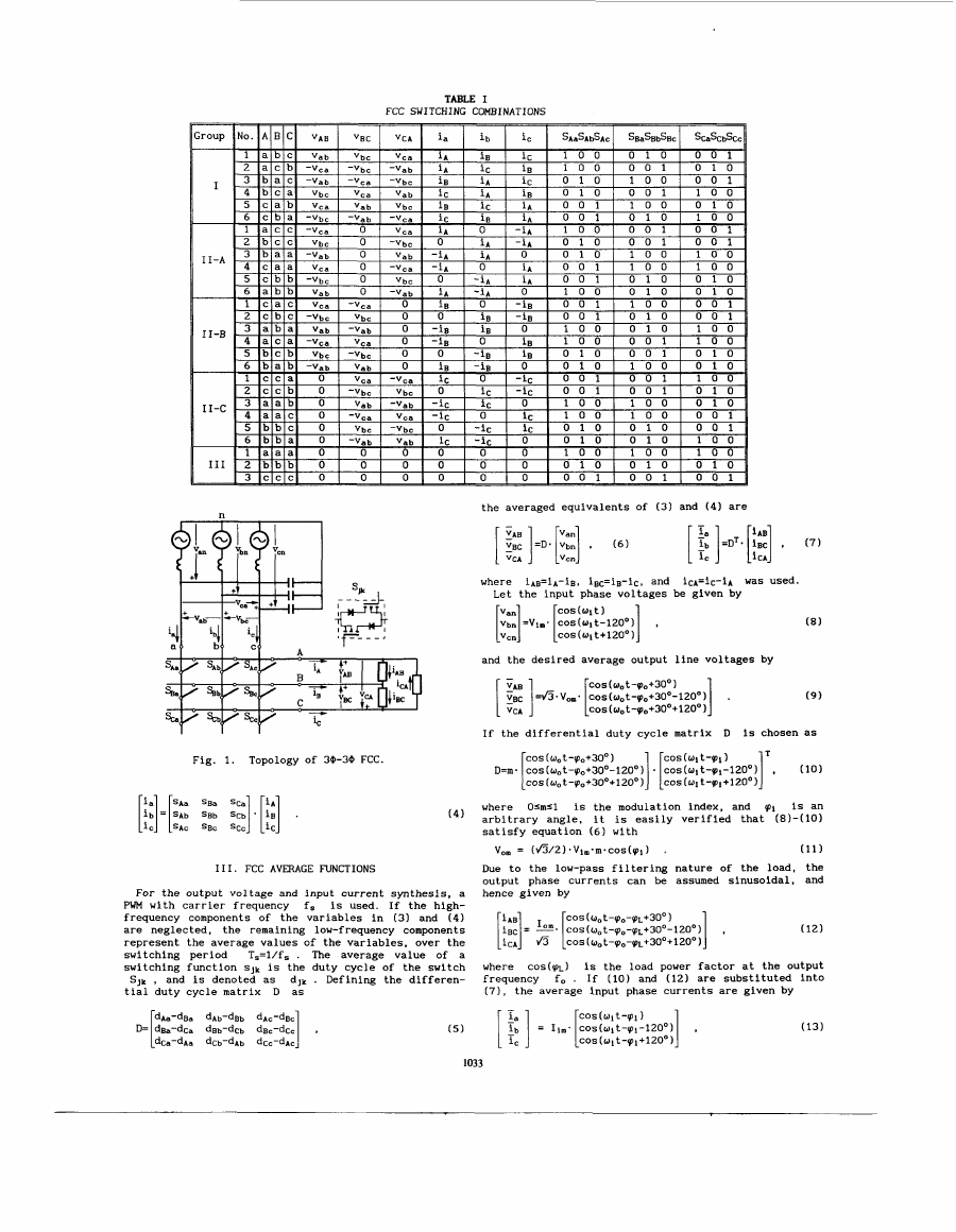
With these constraints, the switches in the FCC from
Fig. 1 can assume only 27 allowed combinations shown in
Table I. The table also shows which input and output
phases are mutually connected for each allowed
switching combination, as well as the resulting output
line voltages and input phase currents. The switching
combinations can be classified into three groups. The
first group includes 6 combinations where each output
phase is connected to a different output phase. In the
second group, there are 3x6=18 combinations with only
two output phases shorted. The third group includes 3
combinations with all three output phases shorted.
From Table I and Fig. 1. the following expressions
for the output line voltages and input phase currents
are directly derived:
( 3 )
�
TABLE I
FCC SWITCHING COMBINATIONS
the averaged equivalents of (3) and ( 4 ) are
where iAB=iA-iB, iBc=iB-ic, and icA=ic-iA was used.
Let the input phase voltages be given by
and the desired average output line voltages by
cos (~,t-p,+30~ 1
COS ( 0, t -po+3O0+ 1 20, 1
( 8 )
( 9 )
If the differential duty cycle matrix D is chosen as
Fig. 1. Topology of 30-30 FCC.
COS (U, t -(po+3O0 1
( 4 )
111. FCC AVERAGE FUNCTIONS
For the output voltage and input current synthesis, a
PUM with carrier frequency f, is used. If the high-
frequency components of the variables in (3) and ( 4 )
are neglected, the remaining low-frequency components
represent the average values of the variables, over the
T,=l/f. . The average value of a
switching period
switching function S J k is the duty cycle of the switch
S J k , and is denoted as d j k . Defining the differen-
tial duty cycle matrix D as
where Osmsl is the modulation index, and p i is an
arbitrary angle, it is easily verified that (8)-(10)
satisfy equation ( 6 ) with
v,.
(11)
Due to the low-pass filtering nature of the load, the
output phase currents can be assumed sinusoidal, and
hence given by
= (fi/2).~i,*m*cos(pl) .
COS (b~~t-~~-cp~+30~)
cos(oot-~,-~L+30"-12O~~
COS (~0t-(p0-~+300+1200
1
(12)
where cos((p~) is the load power factor at the output
frequency f, . If (10) and (12) are substituted into
(71, the average input phase currents are given by
[$I=
I
[ cos (Ui t-(pi+120° 1
cos(wlt-cp1)
1033
11,. cos(oit-(pi-12O0) ,
(13)
�
11, = (fi/2)*Io,.m-cos(~~) .
(14)
where
Since in and (PI in (10) can be independently selec-
ted, it follows from (8). (11) and (13) that the input
displacement angle 'pi and the converter voltage gain
Vo,/V~,
may be freely adjusted. The only restriction
is equality of the input and output active powers,
because from (11) and (14) it follows that
.
(15)
Unity input displacement factor is obtained for 'p1=0 ,
which from (111, with m=l , also results in the maxi-
mum output to input voltage ratio of A/2 .
I~~*cos((P~)~P~
P~=~.V~,.
IV. SWITCH DUTY CYCLES
Desired differential duty cycles are defined in (10).
From (51, (91, (101, and (13) they can be expressed as
-1 5 dlk-djk = m.ylJ'xk 5 1 , ije{AB.BC.CA),
YIJ'~IJ/(~~~o,) , XkzTk/Ilm ,
ke{a,b,c} .
(16)
Because duty cycles of individual switches must be
positive, they cannot be directly solved for from (16).
Instead, they have to be expressed as dlfferent
sinusoidal functions whenever the term Y I J - ~ ~ changes
sign.
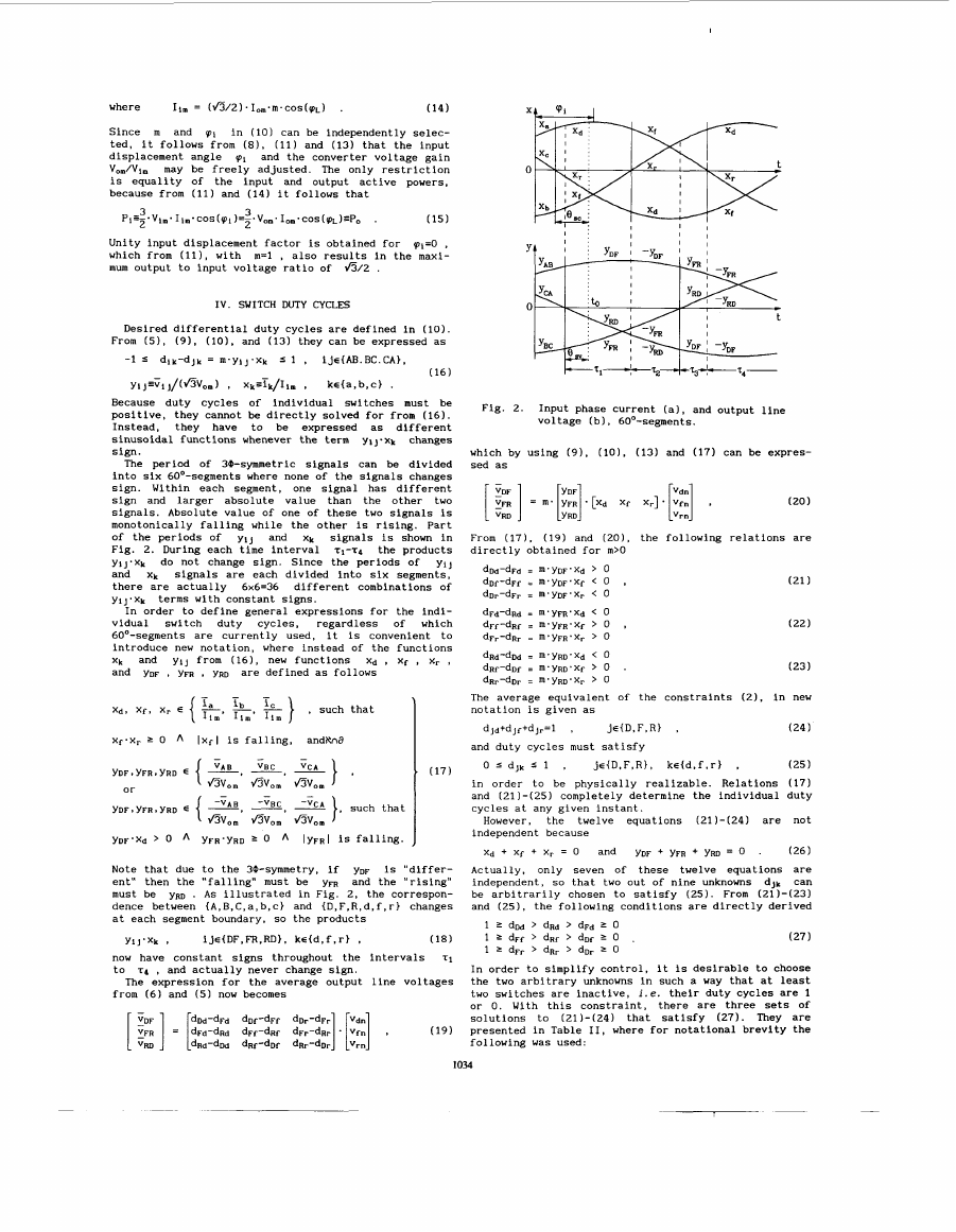
The period of 30-symmetric signals can be divided
into six 60°-segments where none of the signals changes
sign. Within each segment, one signal has different
sign and larger absolute value than the other two
signals. Absolute value of one of these two signals is
monotonically falling while the other is rising. Part
of the periods of Y!J
and xk signals is shown in
Fig. 2. During each time interval ~ 1 - T 4 the products
YlJ'xk do not change sign. Since the periods of Y ~ J
and xk signals are each divided into six segments,
there are actually 6x6=36 different combinations of
ylJ'Xk terms with constant signs.
In order to define general expressions for the indi-
vidual switch duty cycles, regardless of which
60°-segments are currently used, it is convenient to
introduce new notation, where instead of the functions
xk and YIJ from (161, new functions xd , xf , x, ,
and YDF , YFR , YRD are defined as follows
I
Fig. 2. Input phase current (a), and output line
voltage (b), 60°-segments.
which by using (91, (101, (13) and (17) can be expres-
sed as
[
YDF
VDF
i F R ] = m*[yFR]*[xd
VRD
Y RD
xf Xr].
(20)
From (17). (19) and (201, the following relations are
directly obtained for m>O
(21)
(22)
(23)
that
1
The average equivalent of the constraints (21, in new
notation is given as
djd+djf+dJ,=l ,
je{D,F,Rk ,
and duty cycles must satisfy
(24)
* (17)
such that
Note that due to the 3@-symmetry, if YDF is "differ-
ent" then the "falling" must be YFR and the "rising"
must be YRD . As illustrated in Fig. 2. the correspon-
dence between {A,B,C,a,b,c} and {D,F.R,d,f,r) changes
at each segment boundary, so the products
ije{DF,FB.RD). ks{d.f,r} ,
(18)
now have constant signs throughout the intervals T I
to 'c4 , and actually never change sign.
from (6) and (5) now becomes
The expression for the average output line voltages
YIJ'Xk ,
[ iFR ] = IFd-dRd dFf-dRf dFr-dRr]. Lfn]
dDd-dFd dof-dFf dDr-dFr Vdn
(19)
9
VDF
VRD
dRd-dki dRf-dDf dRr-dDr Vrn
0 5 djk 5 1 ,
jc{D,F,R), ke{d,f,r) ,
(25)
in order to be physically realizable. Relations (17)
and (21)-(25) completely determine the individual duty
cycles at any given instant.
However, the twelve equations (21)-(24) are not
independent because
xd + xf + x, = 0
and YDF + YFR + YRD = 0
(26)
Actually, only seven of these twelve equations are
independent, so that two out of nine unknowns dJk can
be arbitrarily chosen to satisfy (25). From (21)-(23)
and (25). the following conditions are directly derived
.
(27)
In order to simplify control, it is desirable to choose
the two arbitrary unknowns in such a way that at least
two switches are inactive, i.e. their duty cycles are 1
or 0. With this constraint, there are three sets of
solutions to (21)-(24) that satisfy (27). They are
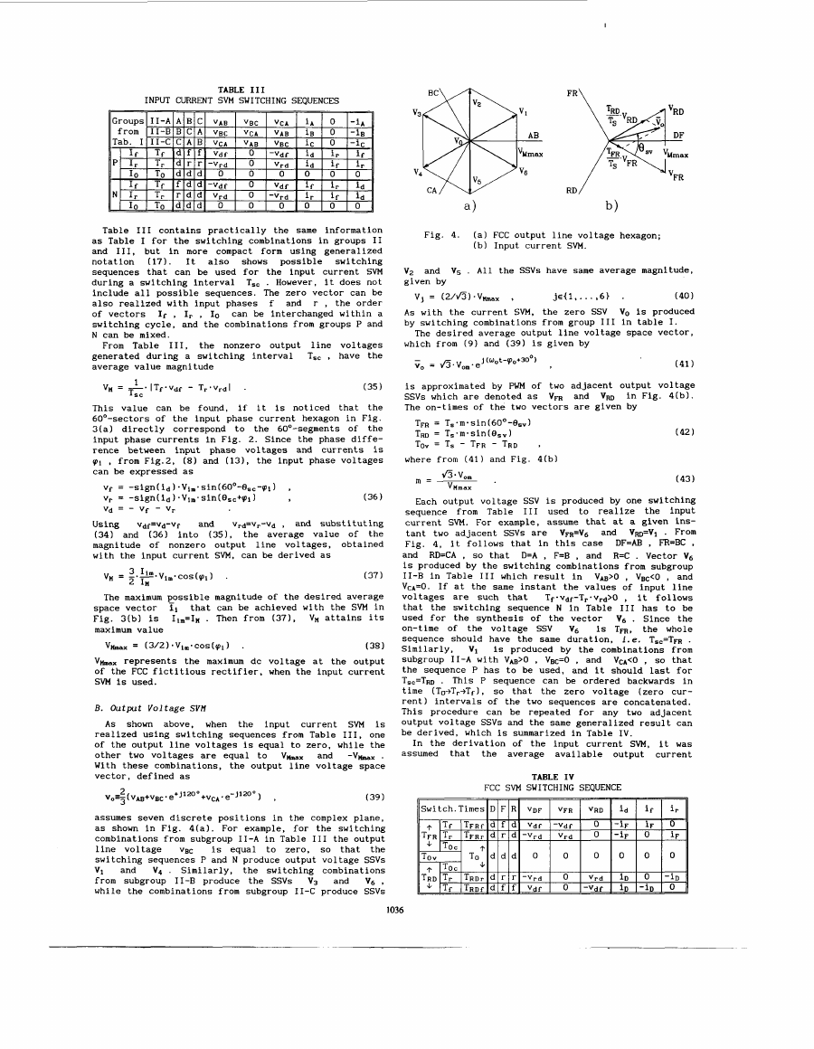
presented in Table 11, where for notational brevity the
following was used:
1034
�
can assume only seven discrete positions in the complex
plane, called the input current switching state vectors
(SSVs), as shown in Fig. 3(a). For example, if the
switching combination 1 from the subgroup 11-A in Table
I is used, the input phase currents are ia=iA , ib=O ,
and ic=-iA , producing the SSV 11 if iA>o and Iq
. Switching combination 4 produces the same
if iA'O
SSVs but for the opposite polarity of i A . The other
four combinations from the same subgroup produce the
remaining four SSVs in Fig. 3(a). All the SSVs have
same magnitude, which from Fig. 3(a) is
ke{l, . . . , 6 ) ,
(32)
where In=liAl . Switching combinations from subgroups
11-B and 11-C produce SSVs in same positions but with
different magnitudes, given by (32) and by In=liel and
IH=liCl, respectively. The switching combinations from
group I 1 1 result in the zero input current SSV IO .
from (13) and (31) is given by
The desired average input current space vector, which
II, = (2/fi)*Ia ,
can be approximated by two adjacent input current SSVs
If and I, , using standard SVM, as shown in Fig.
3(b). The on-times of the SSVs are
Tf = T,,-~~sin(60°-~,,) ,
IH
Tr = T,,*~~sin(B.,)
To= = T,, - Tf - T,
(34)
If the available average output current magnitude In
could be somehow kept constant, the average input phase
currents would be 30 balanced and without low-frequency
harmonics [91. This will be achieved with the output
voltage SVM.
Only two input phases are used to produce an input
current SSV. From Fig. 3(b), the SSV If is obtained
when the input phases d and f are connected to
output phases, while the input phases d and r are
used for the SSV Ir . For example, assume that at a
given instant two adjacent SSVs are
and
Ir=I1 . From Fig. 3 it follows that in this case d=a ,
f=b , and r=c . Vector 16 can be produced by switch-
ing combination 6 in subgroup 11-A from Table I if iA
is positive, or by combination 3 if i A is negative.
It can be also produced by switching combinations 6 or
3 from the subgroups 11-B and 11-C. As seen from Table
I, regardless of a subgroup, combination 6 results in
one output line voltage equal to zero, one to
Vdf(=Vab) , and one to -Vdf , while the combination 3
produces same result with opposite polarity. Similar
analysis can be done for the switching combinations 1
and 4 which produce the SSV I1 . This is summarized in
Table 111. where the switching sequences resulting in
the output voltages of different polarity are labeled
as P and N. This procedure can be repeated for any two
adjacent SSVs and the same generalized result will be
obtained.
Id=I6
dmf = m-YRo.xf
dRDr = m*ym*X, .
dFRf = m.YFR.xf
( 2 8 )
dFRr = m*YFR'Xr '
From the preceding derivation and Fig. 2, the
individual switch duty cycles can be found in the
following way. At a given instant to , the currently
used input phase current and output line voltage seg-
ments can be identified, and the correspondence between
{A,B,C,a,b,c} and {D,F,R,d,f,r} can be found using
definition (17). Since the modulation functions change
only at the boundaries of the segments, instead of the
absolute time t , angles from the beginnings of the
currently used input and output segments can be
employed. These angles, denoted as Os,
respectively, are shown in Fig. 2. It is easily veri-
fied from the figure that
and
e,.,
After substituting ( 2 9 ) into (281, individual duty
cycles can be found from Table I1 for a selected set of
solutions.
( 2 9 )
V. SPACE VECTOR MODULATION
From (20) and (26) it follows that
(30)
i.e. the output line voltages are synthesized by using
only two input line voltages within a switching period
T, . This means that the switching combinations from
the first group in Table I are not used. Because the
switching combinations from the second and third groups
result in one of the output line voltages and one of
the input phase currents equal to zero, they can be
used for output voltage SVM [71, [SI and input current
SVM 191.
A. Input Current SVM
The output line currents can be considered constant
during a short switching interval T,, . Then, for the
switching combinations from groups I1 and I11 in Table
I, the input phase current space vector, defined as
,
i i ~ ~ ( i a + i b . e + J 1 2 0 0 + i c . e - J l ~ o )
3
(31 1
1035
Fig. 3. (a) FCC input phase current hexagon;
(b) Input current SVM.
�
I
FR\
RD/
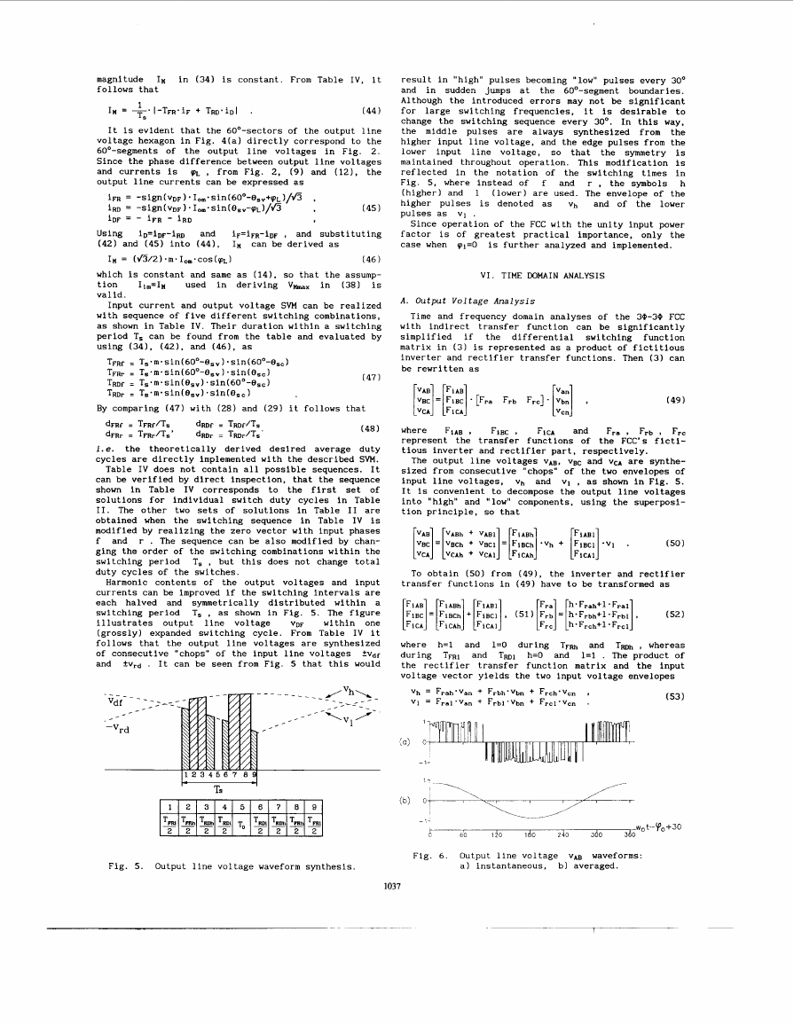
Fig. 4. (a) FCC output line voltage hexagon;
(b) Input current SVM.
Vz and V5 . All the SSVs have same average magnitude,
given by
v, = (2/fi).VW, ,
(40)
As with the current SVM, the zero SSV VO is produced
by switching combinations from group I11 in table I.
je{l, ..., 61 .
The desired average output line voltage space vector,
which from (9) and (39) is given by
is approximated by PUM of two adjacent output voltage
SSVs which are denoted as VFR and Vm in Fig. 4(b).
The on-times of the two vectors are given by
(41 1
TFR = T,~m~~in(60~-6.~)
TRD = T,*m*sin(B,,)
Tov = Ts - TFR - TRD ,
where from (41) and Fig. 4(b)
(42)
Each output voltage SSV is produced by one switching
sequence from Table I11 used to realize the input
current SVM. For example, assume that at a given ins-
tant two adjacent SSVs are VFR=V.5 and Vm=V1 . From
Fig. 4, it follows that in this case DF=AB , FR=BC ,
and RD=CA , so that D=A , F=B , and R=C . Vector v.5
is produced by the switching combinations from subgroup
11-B in Table 111 which result in V&O
, VBC
O , it follows
that the switching sequence N in Table 111 has to be
used for the synthesis of the vector v.5 . Since the
on-time of the voltage SSV v.5
is TFR, the whole
.
sequence should have the same duration, f . e . T.,=TFR
Similarly, V1 is produced by the combinations from
, VBC=O , and Vc.magnitude In in (34) is constant. From Table IV, it
follows that
1
Ts
In = --'I-TFR-~F + Tm*iDI .
(44)
It is evident that the 60°-sectors of the output line
voltage hexagon in Fig. 4(a) directly correspond to the
60°-segments of the output line voltages in Fig. 2.
Since the phase difference between output line voltages
and currents is ca , from Fig. 2, (9) and (12). the
output line currents can be expressed as
iFR = -sign(vDF) ~Io,~sin~600-~.,+~~~/~
iRD = -sign(voF).I,,.sin(B,,-~L)/~
IDF = - iFR - IRD
,
,
(45)
Using iD=iDF-im
(42) and (45) into (441, In can be derived as
and iF=iFR-iDF , and substituting
result in "high" pulses becoming "low" pulses every 30'
and in sudden jumps at the 60°-segment boundaries.
Although the introduced errors may not be significant
for large switching frequencies, it is desirable to
change the switching sequence every 30°. In this way,
the middle pulses are always synthesized from the
higher input line voltage, and the edge pulses from the
lower input line voltage, so that the symmetry is
maintained throughout operation. This modification is
reflected in the notation of the switching times in
Fig. 5, where instead of f and r , the symbols h
(higher) and 1 (lower) are used. The envelope of the
higher pulses is denoted as vh and of the lower
pulses as VI .
Since operation of the FCC with the unity input power
factor is of greatest practical importance, only the
case when cpi=O is further analyzed and implemented.
Ii,=In
In = (fi/2)*m*1,.*cos((~L)
(46)
which is constant and same as (14). so that the assump-
used in deriving V m x in (38) is
tion
valid.
Input current and output voltage SVM can be realized
with sequence of five different switching combinations,
as shown in Table IV. Their duration within a switching
period T, can be found from the table and evaluated by
using (34). (421, and (461, as
TFRf = T,.m. sin (6Oo-B,, * sin (60°-0,,)
TFRr = TS~m~sin(6O0-B,,) -sin(eSc)
TRDf = T,*m.sin(B,,) ~sin(60°-B,,)
T R D ~ = T,.m-sin(B.,)
.sin(e,,)
(47)
By comparing (47) with (28) and (29) it follows that
dFRf = TFRf/Ts
dFRr = TFRrlTs'
dmf = Tmf/Ts,
dmr = Tmr/Ts
(48)
i . e . the theoretically derived desired average duty
cycles are directly implemented with the described SVM.
Table IV does not contain all possible sequences. It
can be verified by direct inspection, that the sequence
shown in Table IV corresponds to the first set of
solutions for individual switch duty cycles in Table
11. The other two sets of solutions in Table I1 are
obtained when the switching sequence in Table IV is
modified by realizing the zero vector with input phases
f and r . The sequence can be also modified by chan-
ging the order of the switching combinations within the
switching period T, , but this does not change total
duty cycles of the switches.
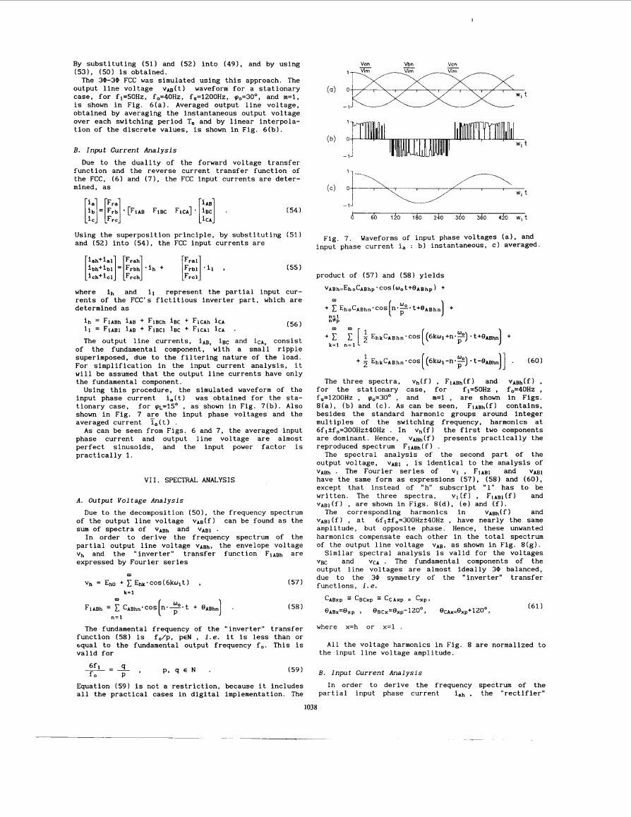
Harmonic contents of the output voltages and input
currents can be improved if the switching intervals are
each halved and symmetrically distributed within a
switching period T, , as shown in Fig. 5. The figure
within one
illustrates output line voltage
(grossly) expanded switching cycle. From Table IV it
follows that the output line voltages are synthesized
of consecutive "chops" of the input line voltages ?Vdf
and +vrd . It can be seen from Fig. 5 that this would
VDF
VI. TIME WMAIN ANALYSIS
A. Output Voltage Analysis
Time and frequency domain analyses of the 39-39 FCC
with indirect transfer function can be significantly
simplified if the differential switching function
matrix in (3) is represented as a product of fictitious
inverter and rectifier transfer functions. Then (3) can
be rewritten as
F ~ B C .
(49)
Fra . Frb . Frc
FIAB ,
where
represent the transfer functions of the FCC's ficti-
tious inverter and rectifier part, respectively.
FICA and
The output line voltages VAB, VBC and VCA are synthe-
sized from consecutive "chops" of the two envelopes of
input line voltages, vh and VI , as shown in Fig. 5 .
It is convenient to decompose the output line voltages
into "high" and "low" components, using the superposi-
tion principle, so that
VABh + "AB1
E!:]=[:;:;
[ii:]=[:::~J+b::::].
"'::]=[::::d'vh
FIABh
FlABh
F ~ A S I
+ k;;;:].vl
.
(50)
To obtain (50) from (491, the inverter and rectifier
transfer functions in (49) have to be transformed as
FIABI (51) li]=b:;L:E;::;L::].
h* Frah+l *Fra1
(52)
where h=l and 1=0 during T F ~ and Tmh , whereas
during TFRI and Tml h=O and 1=1 . The product of
the rectifier transfer function matrix and the input
voltage vector yields the two input voltage envelopes
Fig. 5. Output line voltage waveform synthesis.
Fig. 6. Output line voltage VAB waveforms:
a) instantaneous, b) averaged.
1037
�
I
By substituting (51) and (52) into (49). and by using
(531, (50) is obtained.
The 30-30 FCC was simulated using this approach. The
output line voltage VAB(t.1
waveform for a stationary
case, for fi=50Hz, f0=40Hz, fs=1200Hz, (po=3O0, and m=l,
is shown in Fig. 6(a). Averaged output line voltage,
obtained by averaging the instantaneous output voltage
over each switching period T. and by linear interpola-
tion of the discrete values, is shown in Fig. 6(b).
B. Input Current Analysis
Due to the duality of the forward voltage transfer
function and the reverse current transfer function of
the FCC, (6) and (71, the FCC input currents are deter-
mined, as
(541
Using the superposition principle, by substituting (511
and (52) into (541, the FCC input currents are
Fig. 7. Waveforms of input phase voltages (a), and
input phase current i, : b) instantaneous, c) averaged.
where ih and il represent the partial input cur-
rents of the FCC's fictitious inverter part, which are
determined as
(55)
(56)
ih = FiABh iAB + FiBch iBC + FiCAh iCA
il = F I A B ~ iAB + FiBcl iBc + Fic~i iCA .
The output line currents, iAB, iBc and icA, consist
of the fundamental component, with a small ripple
superimposed, due to the filtering nature of the load.
For simplification in the input current analysis, it
will be assumed that the output line currents have only
the fundamental component.
Using this procedure, the simulated waveform of the
was obtained for the sta-
input phase current i,(t)
tionary case, for (p~=15O , as shown in Fig. 7(b). Also
shown in Fig. 7 are the input phase voltages and the
averaged current i,(t)
As can be seen from Figs. 6 and 7, the averaged input
phase current and output line voltage are almost
perfect sinusoids, and the input power factor is
practically 1.
-
.
VII. SPECTRAL ANALYSIS
A. Output Voltage Analysis
Due to the decomposition (501, the frequency spectrum
of the output line voltage V A B ( ~ ) can be found as the
sum of spectra of VABh and V A B ~ .
In order to derive the frequency spectrum of the
partial output line voltage VABh, the envelope voltage
vh and the "inverter" transfer function FiABh are
expressed by Fourier series
(57)
The three Spectra, Vh(f) , FiABh(f) and VABh(f)
fi=50Hz , f,=4OHz ,
for the stationary case, for
m=l , are shown in Figs.
fS=1200Hz , (po=3O0 , and
8(a), (b) and (c). As can be seen, FlABh(f) contains,
besides the standard harmonic groups around integer
multiples of the switching frequency, harmonics at
6flffo=300Hzf40Hz . In Vh(f) the first two components
are dominant. Hence, VABh(f) presents practically the
reproduced spectrum FiABh(f 1 .
The corresponding harmonics in
The spectral analysis of the second part of the
output voltage, V A B ~ , is identical to the analysis of
VABh . The Fourier series of v1 , F ~ A B ~ and V A B ~
have the same form as expressions (571, (58) and (601,
except that instead of "h" subscript "1" has to be
written. The three spectra, vl(f) , FiABl(f)
and
VABl(f) , are shown in Figs. 8(d), (e) and (f).
VABh(f)
and
v~~l(f) , at 6fl?fO=300Hz?40Hz , have nearly the same
amplitude, but opposite phase. Hence, these unwanted
harmonics compensate each other in the total spectrum
of the output line voltage VAB, as shown in Fig. 8(g).
Similar spectral analysis is valid for the voltages
VCA . The fundamental components of the
VBC
output line voltages are almost ideally 30 balanced,
due to the 30 symmetry of the "inverter" transfer
functions, i.e.
and
CAB^^
eABx=@xp , eBcx=exp-1200, ecAx,exp+1200,
C~cxp e C C A X ~ = Cxp,
(61 1
The fundamental frequency of the "inverter" transfer
function (58) is f,/p, pcN , i . e . it is less than or
equal to the fundamental output frequency fo. This is
valid for
where x=h or x=l .
All the voltage harmonics in Fig. 8 are normalized to
the input line voltage amplitude.
Equation (59) is not a restriction, because it includes
all the practical cases in digital implementation. The
In order to derive the frequency spectrum of the
i&, , the "rectifier"
partial input phase current
(59)
B. Input Current Analysis
1038
�
ih(f)
ples of the switching frequency, a harmonic at
6fl=300Hz . The spectrum i&(f) , in the critical
.
frequency range is mainly proportional to F,,h(f)
This is evident from the fact that the 300Hz component
Fr,h(f) ,
of
harmonics at frequencies fi and (6jtl)-fl , JEN .
phase current, i,l
iah . The three spectra,
i,l(fI
The spectral analysis of the second part of the input
, is identical to the analysis of
and
, are shown in Figs. 9(d), (e) and (f).
produces, when multiplied by
F,,l(f) , il(f)
lsbo
2ab0
560
0.0
1 .o
lab0
0.0 J
(b) 0.5
2sbo d m f(W
1 .o L
(c)0,5L
0.0 1 .o (d)0.5j
0.0 1 .o (e)0.51
Again, as in the output voltage case, the correspon-
and i.l(f) , at the Criti-
ding harmonics in i&(f)
cal frequencies 6flffi=300Hz~50Hz , have nearly the
same amplitude, but opposite phase. Hence, these unwan-
ted harmonics compensate each other in the total spec-
trum of the input phase current i, , Fig. 9 ( g ) .
All the current harmonics in Fig. 9 are normalized to
the amplitude of the output line current fundamental
component.
compute the switching times according t o (471,
convert the switching times to switching pulses,
The FCC space vector modulator has to perform the
VIII. DIGITAL IMPLEMENTATION
following tasks:
* distribute the switching pulses to individual
4QSWs, based on the currently used input voltage
30°-segment and output voltage 6O0-segment.
0.0 1 .o
(9 0.0 0
1.0,
11
(9) 0.5
.
5
0.0
560
II I..
15bo
lobo
I I I I , .
2sbo
zdoo
3obo f ( M )
Fig. 8 . Frequency spectrum of
(a) Input voltage envelope vh ,
(b) Fictitious inverter transfer functions FlABh,
( c ) Partial output line voltage VABh ,
(d) Input Voltage Envelope vi ,
(e) Fictitious Inverter Transfer Function F ~ A B ~
(fl Partial Output Line Voltage V A B ~ ,
( g ) Total Output Line Voltage VAB .
,
transfer function Frah is expressed by Fourier series:
C;~-cos((6k-l)qt) . (62)
1
Frah=Cahl'COS(Wit) +
E (C:hr*coS((6k+l)olt)+
+
k= 1
~
,
,lbbo,,
,,,
,
,
,
1500
zoo0 2500
YJoOf(H2)
, ,
(a)::],
~
0.0
1 .o
(b) 0.5
0.0
0.0
(4
0.0
(e) 0.5
"O
1
By substituting ( 5 8 ) into (56). and using (611, the
partial input current of the FCC's "inverter" part is
obtained
3
2
ih = - ' c h ~ ' c o ~ ( ( p ~ + ( p L - 3 0 ° ~ ~ ~ ~ )
+
[ i
( - - i).~,t
+ ~ i , . ~ ~ ~
+ ei,,
11
.
(63)
Multiplication of (62) by (63) yields the FCC partial
iah . The three spectra,
input phase current
F,,h(f)
, ih(f) and i,h(f) , for the stationary case,
for (p~=15' , are shown in Figs. 9(a), (b) and (c). As
can be seen, ih(f) contains, besides the dc component
and the standard harmonic group around integer multi-
1039
Fig. 9. Frequency spectrum of
(a) Fictitious rectifier transfer function Frah ,
(b) Fictitious inverter input current ih ,
(c) Partial input phase current iah ,
(d) Fictitious rectifier transfer function Fral ,
(e) Fictitious inverter input current il ,
(f) Partial input phase current i a l ,
(g) Total input phase current i, .
�


 2023年江西萍乡中考道德与法治真题及答案.doc
 2012年重庆南川中考生物真题及答案.doc
 2013年江西师范大学地理学综合及文艺理论基础考研真题.doc
 2020年四川甘孜小升初语文真题及答案I卷.doc
 2020年注册岩土工程师专业基础考试真题及答案.doc
 2023-2024学年福建省厦门市九年级上学期数学月考试题及答案.doc
 2021-2022学年辽宁省沈阳市大东区九年级上学期语文期末试题及答案.doc
 2022-2023学年北京东城区初三第一学期物理期末试卷及答案.doc
 2018上半年江西教师资格初中地理学科知识与教学能力真题及答案.doc
 2012年河北国家公务员申论考试真题及答案-省级.doc
 2020-2021学年江苏省扬州市江都区邵樊片九年级上学期数学第一次质量检测试题及答案.doc
 2022下半年黑龙江教师资格证中学综合素质真题及答案.doc