011
Analog design is art and sci-
ence at the same time.
It is art because it requires
creativity to strike the right
compromises between the
specifications imposed and
the ones forgotten.
It is also science because
it requires a certain level of
methodology to carry out a
design, inevitably leading to
more insight in the compro-
mises taken.
This book is a guide
through
this wonderful
world of art and science. It
claims to provide the novice designers with all aspects of analog design, which are essential to
this understanding.
As teaching is the best way to learn, all slides are added on a CD-ROM, with and without
the comments added as notes in the pdf files. The reader is suggested to try to explain parts of
this course to his fellow designers. This is the way to experience and to cultivate the circles of
art and science embedded in this book.
All design is about circuits. All circuits contain transistors. Hand-models are required of these
devices in order to be able to predict circuit performance. CAD tools such as SPICE, ELDO,
SPECTRE, etc. are then used to verify the predicted performance. This feedback loop is essential
to converge to a real design. This loop will be used continuously in this book.
by means
012
For the design of analog
integrated circuits, we need
to be able to predict the per-
formance
of
simple expressions. As a
result,
simple models are
required. This means that
the small-signal operation of
each transistor must be
described by means of as
few equations as possible.
Clearly the performance of
the circuit can then only be
described in an approximate
way. The main advantage
however,
is that transistor
1
�
2
Chapter #1
sizing and current levels can easily be derived from such simple expressions. They can then be
used to simulate the circuit performance by means of a conventional circuit simulator such as
SPICE or ELDO.
In these simulators, models are used which are much more accurate but also much more
complicated. These simulations are required afterwards to verify the circuit performance. The
initial design with simple models is the first step in the design procedure. They are aimed
indeed at the determination of all transistor currents and sizes, according to the specifications
imposed.
We start with MOST devices, although the bipolar transistor are historically first. Nowadays
the number of MOS transistors integrated on chips, vastly outnumber the bipolar ones.
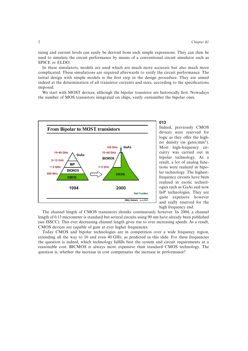
013
Indeed, previously CMOS
devices were reserved for
logic as they offer the high-
est density (in gates/mm2).
Most high-frequency cir-
cuitry was carried out
in
technology. As a
bipolar
result, a lot of analog func-
tions were realized in bipo-
lar technology. The highest-
frequency circuits have been
realized in exotic technol-
ogies such as GaAs and now
InP technologies. They are
quite
expensive however
and really reserved for the
high frequency end.
The channel length of CMOS transistors shrinks continuously however. In 2004, a channel
length of 0.13 micrometer is standard but several circuits using 90 nm have already been published
(see ISSCC). This ever decreasing channel length gives rise to ever increasing speeds. As a result,
CMOS devices are capable of gain at ever higher frequencies.
Today CMOS and bipolar technologies are in competition over a wide frequency region,
extending all the way to 10 and even 40 GHz, as predicted in this slide. For these frequencies
the question is indeed, which technology fulfills best the system and circuit requirements at a
reasonable cost. BICMOS is always more expensive than standard CMOS technology. The
question is, whether the increase in cost compensates the increase in performance?
�
Comparison of MOST and bipolar transistors
3
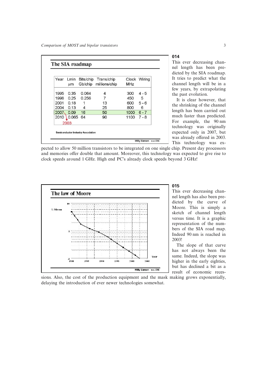
014
This ever decreasing chan-
nel
length has been pre-
dicted by the SIA roadmap.
It tries to predict what the
channel length will be in a
few years, by extrapolating
the past evolution.
It is clear however, that
the shrinking of the channel
length has been carried out
much faster than predicted.
For
the 90 nm
technology was originally
expected only in 2007, but
was already offered in 2003.
This
technology was ex-
pected to allow 50 million transistors to be integrated on one single chip. Present day processors
and memories offer double that amount. Moreover, this technology was expected to give rise to
clock speeds around 1 GHz. High end PC’s already clock speeds beyond 3 GHz!
example,
015
This ever decreasing chan-
nel length has also been pre-
dicted by the
curve of
Moore. This is simply a
sketch of channel
length
versus time. It is a graphic
representation of the num-
bers of the SIA road map.
Indeed 90 nm is reached in
2003!
The slope of that curve
has not always been the
same. Indeed, the slope was
higher in the early eighties,
but has declined a bit as a
result of economic reces-
sions. Also, the cost of the production equipment and the mask making grows exponentially,
delaying the introduction of ever newer technologies somewhat.
�
4
Chapter #1
To
explore
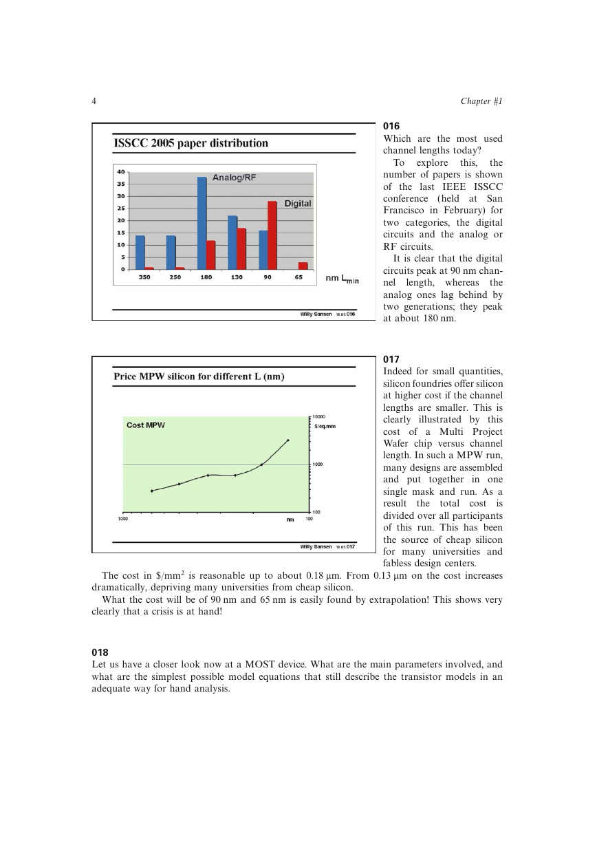
016
Which are the most used
channel lengths today?
this,
the
number of papers is shown
of
the last IEEE ISSCC
( held at San
conference
Francisco in February)
for
two categories, the digital
circuits and the analog or
RF circuits.
length, whereas
It is clear that the digital
circuits peak at 90 nm chan-
nel
the
analog ones lag behind by
two generations; they peak
at about 180 nm.
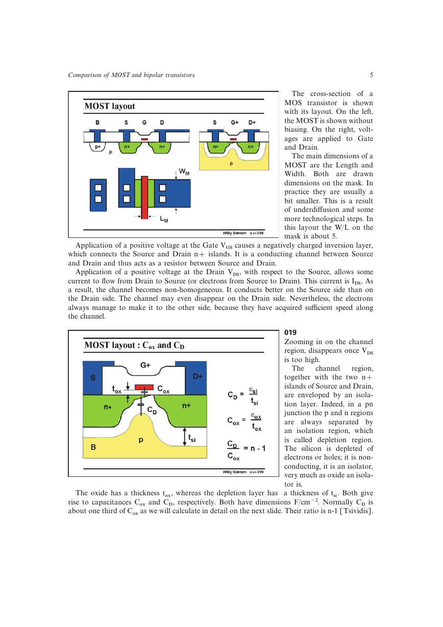
017
Indeed for small quantities,
silicon foundries offer silicon
at higher cost if the channel
lengths are smaller. This is
clearly illustrated by this
cost of a Multi Project
Wafer chip versus channel
length. In such a MPW run,
many designs are assembled
and put
in one
single mask and run. As a
result
is
divided over all participants
of this run. This has been
the source of cheap silicon
for many universities and
fabless design centers.
The cost in $/mm2 is reasonable up to about 0.18 mm. From 0.13 mm on the cost increases
together
total
the
cost
dramatically, depriving many universities from cheap silicon.
What the cost will be of 90 nm and 65 nm is easily found by extrapolation! This shows very
clearly that a crisis is at hand!
018
Let us have a closer look now at a MOST device. What are the main parameters involved, and
what are the simplest possible model equations that still describe the transistor models in an
adequate way for hand analysis.
�
Comparison of MOST and bipolar transistors
5
The cross-section of a
MOS transistor is shown
with its layout. On the left,
the MOST is shown without
biasing. On the right, volt-
ages are applied to Gate
and Drain.
The main dimensions of a
MOST are the Length and
Width. Both are drawn
dimensions on the mask. In
practice they are usually a
bit smaller. This is a result
of underdiffusion and some
more technological steps. In
this layout the W/L on the
mask is about 5.
Application of a positive voltage at the Gate VGS causes a negatively charged inversion layer,
which connects the Source and Drain n+ islands. It is a conducting channel between Source
and Drain and thus acts as a resistor between Source and Drain.
Application of a positive voltage at the Drain VDS, with respect to the Source, allows some
current to flow from Drain to Source (or electrons from Source to Drain). This current is IDS. As
a result, the channel becomes non-homogeneous. It conducts better on the Source side than on
the Drain side. The channel may even disappear on the Drain side. Nevertheless, the electrons
always manage to make it to the other side, because they have acquired sufficient speed along
the channel.
019
Zooming in on the channel
region, disappears once VDS
is too high.
The
channel
region,
together with the two n+
islands of Source and Drain,
are enveloped by an isola-
tion layer. Indeed, in a pn
junction the p and n regions
are always
separated by
an isolation region, which
is called depletion region.
The silicon is depleted of
electrons or holes; it is non-
conducting, it is an isolator,
very much as oxide an isola-
tor is.
The oxide has a thickness tox, whereas the depletion layer has a thickness of tsi. Both give
2. Normally CD is
rise to capacitances Cox and CD, respectively. Both have dimensions F/cm−
about one third of Cox as we will calculate in detail on the next slide. Their ratio is n-1 [Tsividis].
�
6
Chapter #1
It is mportant, however, to note that the channel inversion layer is coupled to the Gate by
means of Cox, but as much coupled to the Bulk by CD. Changing the Gate voltage will thus
change the conductivity of the channel and hence the current IDS. In a similar way, changing
the Bulk voltage will thus also change the conductivity of the channel and will thus change the
current IDS as well. The top gate gives the MOST operation, whereas the bulk gives JFET
operation. Indeed, a Junction FET is by definition a FET in which the current is controlled by
a junction capacitance.
All MOST devices are thus parallel combinations of MOSTs and JFETs. We normally use
only the MOST whereas the JFET is called the body effect, and is treated as a parasitic effect.
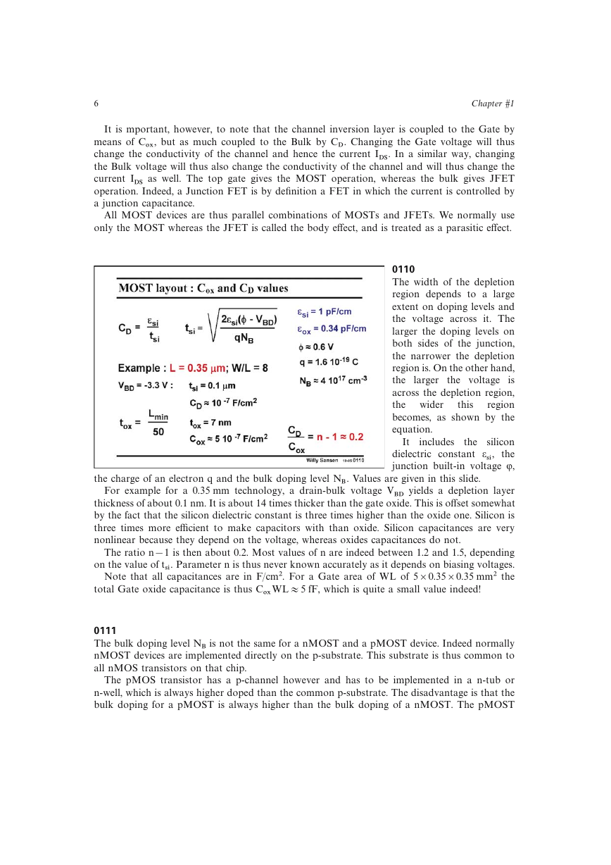
0110
The width of the depletion
region depends to a large
extent on doping levels and
the voltage across it. The
larger the doping levels on
both sides of the junction,
the narrower the depletion
region is. On the other hand,
the larger
the voltage is
across the depletion region,
the wider
region
becomes, as shown by the
equation.
this
It
the
includes
silicon
dielectric constant esi, the
junction built-in voltage Q,
the charge of an electron q and the bulk doping level NB. Values are given in this slide.
For example for a 0.35 mm technology, a drain-bulk voltage VBD yields a depletion layer
thickness of about 0.1 nm. It is about 14 times thicker than the gate oxide. This is offset somewhat
by the fact that the silicon dielectric constant is three times higher than the oxide one. Silicon is
three times more efficient to make capacitors with than oxide. Silicon capacitances are very
nonlinear because they depend on the voltage, whereas oxides capacitances do not.
The ratio n−1 is then about 0.2. Most values of n are indeed between 1.2 and 1.5, depending
on the value of tsi. Parameter n is thus never known accurately as it depends on biasing voltages.
Note that all capacitances are in F/cm2. For a Gate area of WL of 5×0.35×0.35 mm2 the
total Gate oxide capacitance is thus CoxWL#5 fF, which is quite a small value indeed!
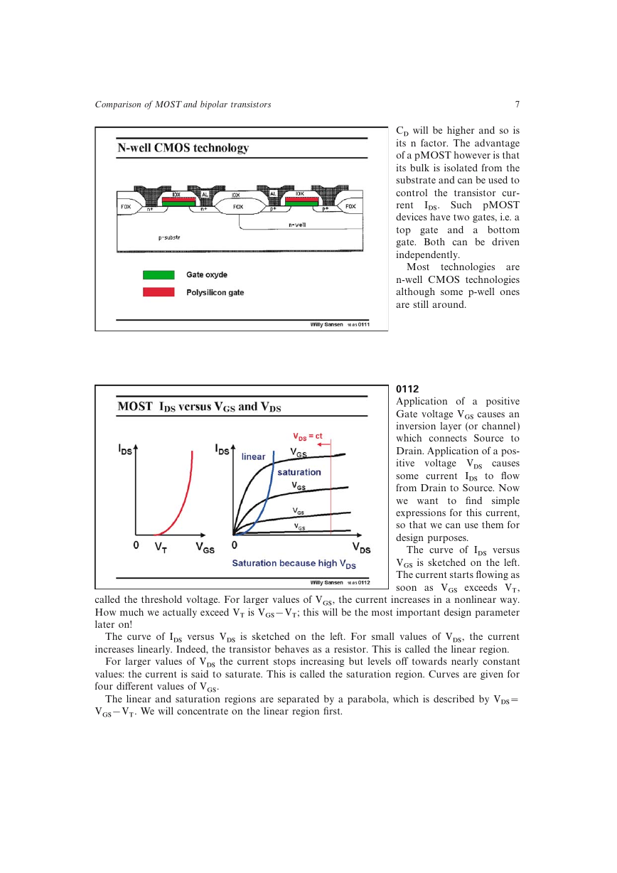
0111
The bulk doping level NB is not the same for a nMOST and a pMOST device. Indeed normally
nMOST devices are implemented directly on the p-substrate. This substrate is thus common to
all nMOS transistors on that chip.
The pMOS transistor has a p-channel however and has to be implemented in a n-tub or
n-well, which is always higher doped than the common p-substrate. The disadvantage is that the
bulk doping for a pMOST is always higher than the bulk doping of a nMOST. The pMOST
�
Comparison of MOST and bipolar transistors
7
CD will be higher and so is
its n factor. The advantage
of a pMOST however is that
its bulk is isolated from the
substrate and can be used to
control the transistor cur-
IDS. Such pMOST
rent
devices have two gates, i.e. a
top gate and a bottom
gate. Both can be driven
independently.
Most
technologies
are
n-well CMOS technologies
although some p-well ones
are still around.
0112
Application of a positive
Gate voltage VGS causes an
inversion layer (or channel )
which connects Source to
Drain. Application of a pos-
itive voltage VDS
causes
some current IDS
to flow
from Drain to Source. Now
we want
to find simple
expressions for this current,
so that we can use them for
design purposes.
The curve of IDS versus
VGS is sketched on the left.
The current starts flowing as
soon as VGS exceeds VT,
called the threshold voltage. For larger values of VGS, the current increases in a nonlinear way.
How much we actually exceed VT is VGS−VT; this will be the most important design parameter
later on!
The curve of IDS versus VDS is sketched on the left. For small values of VDS, the current
increases linearly. Indeed, the transistor behaves as a resistor. This is called the linear region.
For larger values of VDS the current stops increasing but levels off towards nearly constant
values: the current is said to saturate. This is called the saturation region. Curves are given for
four different values of VGS.
The linear and saturation regions are separated by a parabola, which is described by VDS=
VGS−VT. We will concentrate on the linear region first.
�
8
Chapter #1
applications
0113
In many
a
MOST is simply used as a
switch. Its voltage VDS
is
then very small. The MOST
is
then operating in the
linear
region (sometimes
called the ohmic region). In
this region the MOST tran-
sistor is really a small resis-
tor.
It provides a linear
voltage-current characteris-
tic. The channel has the
same conductivity at both
sides – the Source side and
the Drain side.
Let us investigate what
the actual resistance then is.
0114
Zooming in on the corner,
for very small values of VDS,
we find that
indeed the
IDS−VDS curves are very
linear. The MOST behaves
as a pure resistor.
The resistance value Ron
is given in this slide. In addi-
tion to the dimensions W
and L,
technological
parameter appears, called
KP.
a
This parameter character-
izes a certain CMOS tech-
nology as will be explained
on the next slide. Its dimen-
sion is A/V2.
It is clear that the transistor turns very nonlinear when we apply larger VDS voltages. The
crossover value towards the saturation is reached for VDS=VGS−VT, or more accurately for
VDS=( VGS−VT)/n. We will drop this factor n however, as a kind of safety factor. We will, from
now on, assume that a transistor is operating in the saturation region provided VDS>VGS−VT.
0115
For sake of illustration let us a have a closer look at this resistor ‘‘in the corner’’. For this
purpose we have to find an easy approximation for KP. It is given in this slide. Factor b (Greek
beta) contains both the parameter KP and the dimensions of the resistor W and L.
Actually, KP contains the oxide capacitance Cox, and the mobility m (Greek mu). This factor
�



 2023年江西萍乡中考道德与法治真题及答案.doc
 2012年重庆南川中考生物真题及答案.doc
 2013年江西师范大学地理学综合及文艺理论基础考研真题.doc
 2020年四川甘孜小升初语文真题及答案I卷.doc
 2020年注册岩土工程师专业基础考试真题及答案.doc
 2023-2024学年福建省厦门市九年级上学期数学月考试题及答案.doc
 2021-2022学年辽宁省沈阳市大东区九年级上学期语文期末试题及答案.doc
 2022-2023学年北京东城区初三第一学期物理期末试卷及答案.doc
 2018上半年江西教师资格初中地理学科知识与教学能力真题及答案.doc
 2012年河北国家公务员申论考试真题及答案-省级.doc
 2020-2021学年江苏省扬州市江都区邵樊片九年级上学期数学第一次质量检测试题及答案.doc
 2022下半年黑龙江教师资格证中学综合素质真题及答案.doc