ANIP9931E
Calculation of major IGBT operating parameters
CALCULATION OF MAJOR IGBT OPERATING
PARAMETERS
This application note covers how to calculate major IGBT operating parameters
- power dissipation;
-
-
-
- pulsed collector current
in a user specified environment using the datasheet as a source for device characteristics.
continuous collector current;
total power losses;
junction temperature & heatsink;
CONTENTS
1 Calculation of power dissipation .........................................................................................2
2 Calculation of maximum continuous collector current........................................................3
3 Calculation of power losses .................................................................................................6
3.1 Conduction losses..........................................................................................................7
3.2
Switching losses ............................................................................................................9
Total power losses.......................................................................................................16
3.3
4 Calculation of junction temperature and heatsink .............................................................17
5 Calculation of junction temperature and power losses ......................................................19
6 Calculation of pulsed collector current ..............................................................................20
7
Safe operating area.............................................................................................................23
www.infineon.com
1
August-99
�
Infineon
Technologies
ANIP9931E
Calculation of major IGBT operating parameters
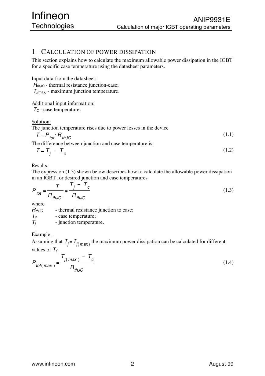
1 CALCULATION OF POWER DISSIPATION
This section explains how to calculate the maximum allowable power dissipation in the IGBT
for a specific case temperature using the datasheet parameters.
Input data from the datasheet:
RthJC - thermal resistance junction-case;
Tj(max) - maximum junction temperature.
Additional input information:
TC - case temperature.
.P
tot
Solution:
The junction temperature rises due to power losses in the device
D T
The difference between junction and case temperature is
D T T
j
T
c
R
thJC
(1.1)
(1.2)
Results:
The expression (1.3) shown below describes how to calculate the allowable power dissipation
in an IGBT for desired junction and case temperatures
D T
RthJC
Tj Tc
RthJC
- thermal resistance junction to case;
- case temperature;
- junction temperature.
Ptot
where
RthJC
Tc
Tj
(1.3)
Example:
Assuming that Tj Tj(
values of TC
)max the maximum power dissipation can be calculated for different
Ptot(
)max
Tc
Tj(
)max
RthJC
(1.4)
www.infineon.com
2
August-99
�
Infineon
Technologies
ANIP9931E
Calculation of major IGBT operating parameters
Figure 1.1 shows the maximum power dissipation for an IGBT as a function of case
temperature.
Parameters in this example:
RthJC = 0.7 K/W;
Tj(max) = 150 C.
Figure 1.1: Power dissipation of SGP20N60.
2 CALCULATION OF MAXIMUM CONTINUOUS COLLECTOR
CURRENT
This section illustrates how to calculate the maximum continuous collector current of IGBT
for a specific case temperature using the datasheet parameters.
Input data from the datasheet:
RthJC - thermal resistance junction-case;
Tj(max) - maximum junction temperature;
output characteristic at Tj(max).
Additional input information:
TC - case temperature.
.Ic Vce
Solution:
The conduction power losses during the on-state of IGBT is the product of the collector
current and the collector-emitter voltage drop at this desired current level.
Pcond
Collector-emitter saturation voltage depends on the collector current flowing through the
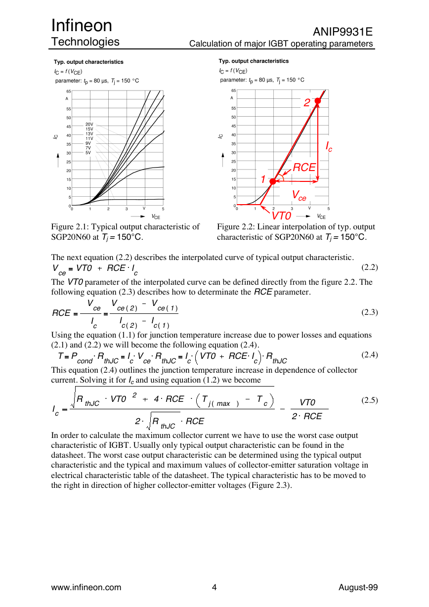
IGBT. The output characteristic of IGBT at maximum junction temperature (Figure 2.1) can
be used to calculate the conduction losses for different current levels. In order to simplify the
analysis the output characteristic for a given gate-emitter voltage will be linearly interpolated
(Figure 2.2).
(2.1)
www.infineon.com
3
August-99
�
Infineon
Technologies
ANIP9931E
Calculation of major IGBT operating parameters
2
D Ic
1
RCE
D Vce
Figure 2.1: Typical output characteristic of
SGP20N60 at Tj = 150 C.
VT0
Figure 2.2: Linear interpolation of typ. output
characteristic of SGP20N60 at Tj = 150 C.
The next equation (2.2) describes the interpolated curve of typical output characteristic.
Vce VT0
The VT0 parameter of the interpolated curve can be defined directly from the figure 2.2. The
following equation (2.3) describes how to determinate the RCE parameter.
.RCE Ic
(2.2)
RCE
D Vce
D Ic
Vce(
Ic(
)2 Vce(
)1
)2
Ic(
)1
(2.3)
Using the equation (1.1) for junction temperature increase due to power losses and equations
(2.1) and (2.2) we will become the following equation (2.4).
D T
.RCE I
c
This equation (2.4) outlines the junction temperature increase in dependence of collector
current. Solving it for Ic and using equation (1.2) we become
.P
cond
VT0
.I
c
.I
c
V
.
ce
.
R
thJC
R
thJC
R
thJC
(2.4)
Ic
RthJC VT0 2
.
.4 RCE Tj(
.
)max
Tc
.2 RthJC RCE
.
VT0
.2 RCE
(2.5)
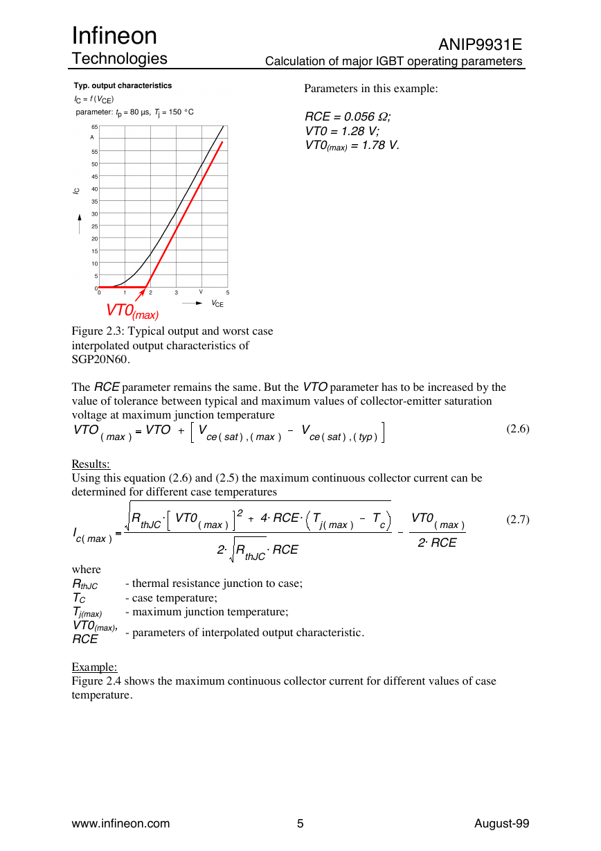
In order to calculate the maximum collector current we have to use the worst case output
characteristic of IGBT. Usually only typical output characteristic can be found in the
datasheet. The worst case output characteristic can be determined using the typical output
characteristic and the typical and maximum values of collector-emitter saturation voltage in
electrical characteristic table of the datasheet. The typical characteristic has to be moved to
the right in direction of higher collector-emitter voltages (Figure 2.3).
www.infineon.com
4
August-99
�
Infineon
Technologies
ANIP9931E
Calculation of major IGBT operating parameters
Parameters in this example:
RCE = 0.056 W ;
VT0 = 1.28 V;
VT0(max) = 1.78 V.
VT0(max)
Figure 2.3: Typical output and worst case
interpolated output characteristics of
SGP20N60.
The RCE parameter remains the same. But the VTO parameter has to be increased by the
value of tolerance between typical and maximum values of collector-emitter saturation
voltage at maximum junction temperature
VTO(
)max VTO V
)max
)sat
typ
)
)sat
ce(
,
(
V
ce(
,
(
Results:
Using this equation (2.6) and (2.5) the maximum continuous collector current can be
determined for different case temperatures
.RthJC VT0(
)max
2
.
.4 RCE Tj(
.
.2 RthJC RCE
)max
Tc
VT0(
)max
.2 RCE
- thermal resistance junction to case;
- case temperature;
- maximum junction temperature;
- parameters of interpolated output characteristic.
Ic(
)max
where
RthJC
TC
Tj(max)
VT0(max),
RCE
(2.6)
(2.7)
Example:
Figure 2.4 shows the maximum continuous collector current for different values of case
temperature.
www.infineon.com
5
August-99
�
Infineon
Technologies
ANIP9931E
Calculation of major IGBT operating parameters
Parameters in this example:
RCE = 0.056 W ;
RthJC = 0.7 K/W;
Tj(max) = 150 C;
VT0(max) = 1.78 V.
Figure 2.4: Continuous collector current of
SGP20N60.
3 CALCULATION OF POWER LOSSES
This section explains how to calculate the conduction and switching power losses in the IGBT
from the actual circuit, including the current waveform, voltage and operating frequency
using the datasheet parameters.
Input data from the datasheet:
output characteristic at Tj(max);
collector-emitter saturation voltage vs. junction temperature;
switching losses vs. collector current at Tj(max);
switching losses vs. gate resistor at Tj(max);
switching losses vs. junction temperature.
- duty cycle;
Additional input information:
D
dic
dt
f
Qrr, trr
TC
Tj
tp
RG
VDC(on)
VDC(off)
- collector current turn on transient rate;
- switching frequency;
- parameters of the user specific diode at these operation conditions;
- case temperature;
- junction temperature;
- pulse length;
- gate resistor;
- DC voltage at IGBT during the off state before the beginning of the turn-on
transition;
- DC voltage at IGBT after the end of the turn-off transition.
www.infineon.com
6
August-99
�
Infineon
Technologies
ANIP9931E
Calculation of major IGBT operating parameters
Solution:
The energy dissipated in the IGBT can be obtained with the following expression
E tot
t
p
0
.vce ic
d
t
(3.1)
.E tot f
where tp is the pulse length. Power is obtained by multiplying by frequency, for repetitive
switching waveforms
P tot
In order to simplify the analysis the total power losses can be divided into conduction and
switching losses
Ptot Pcond
The losses during the off state of transistor are negligible and will be not discussed.
Pswitch
(3.2)
(3.3)
3.1 Conduction losses
Conduction losses occur between the end of the turn-on transition and the beginning of the
turn-off transition. Using the equation 3.1 and interpolated output characteristic at Tj(max)
(equation 2.2) the conduction losses can be calculated for different waveforms of collector
current.
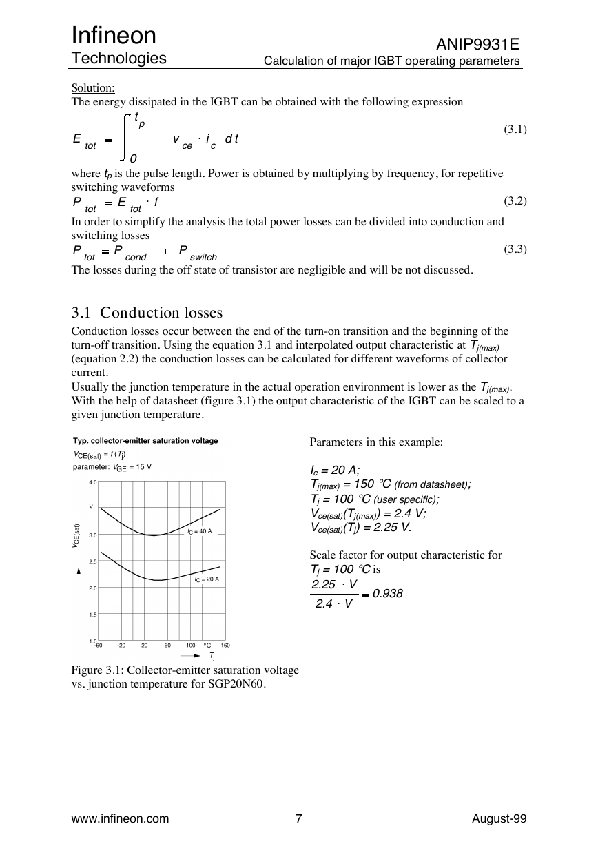
Usually the junction temperature in the actual operation environment is lower as the Tj(max).
With the help of datasheet (figure 3.1) the output characteristic of the IGBT can be scaled to a
given junction temperature.
Parameters in this example:
Ic = 20 A;
Tj(max) = 150 C (from datasheet);
Tj = 100 C (user specific);
Vce(sat)(Tj(max)) = 2.4 V;
Vce(sat)(Tj) = 2.25 V.
Scale factor for output characteristic for
Tj = 100 C is
.
2.25 V
.2.4 V
0.938
Figure 3.1: Collector-emitter saturation voltage
vs. junction temperature for SGP20N60.
www.infineon.com
7
August-99
�
Infineon
Technologies
ANIP9931E
Calculation of major IGBT operating parameters
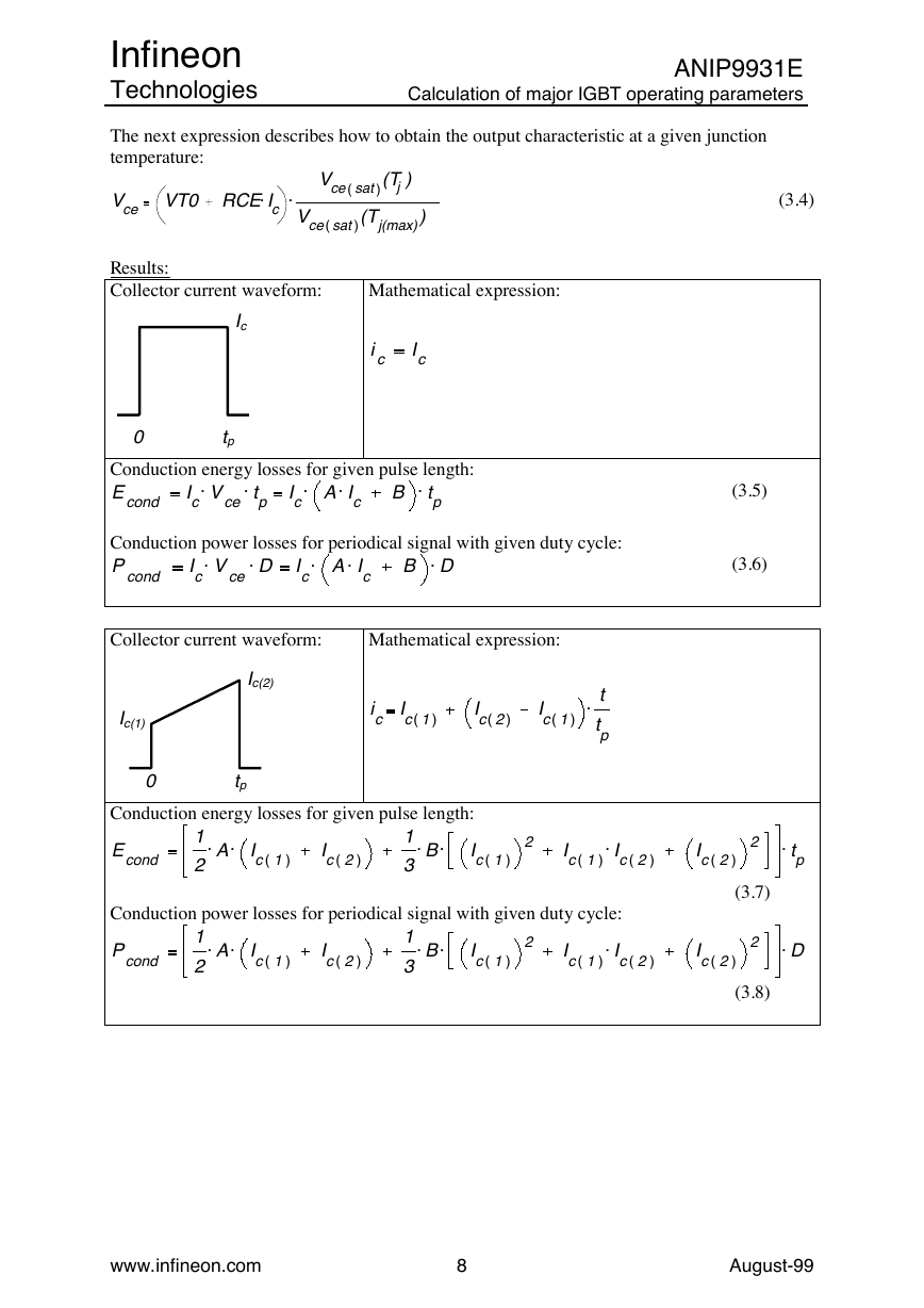
The next expression describes how to obtain the output characteristic at a given junction
temperature:
Vce
VT0
.RCEIc
.
)sat (T )j
Vce(
)sat (T )
j(max)
Vce(
Results:
Collector current waveform:
Mathematical expression:
Ic
ic
Ic
0
tp
Conduction energy losses for given pulse length:
Econd
.A Ic B tp
.Ic Vce tp
.Ic
.
.
Conduction power losses for periodical signal with given duty cycle:
Pcond
.A Ic B D
.Ic Vce D
.Ic
.
.
(3.4)
(3.5)
(3.6)
Collector current waveform:
Mathematical expression:
Ic(2)
Ic(1)
0
tp
ic Ic(
)1
Ic(
)2
Ic(
)1
.
t
tp
Conduction energy losses for given pulse length:
Econd
.1
2
.
A Ic(
)1
Ic(
)2
.1
3
.
B Ic(
)1
2
Ic(
.
)1 Ic(
)2
2
Ic(
)2
.
tp
Conduction power losses for periodical signal with given duty cycle:
Pcond
.1
2
.
A Ic(
)1
Ic(
)2
.1
3
.
B Ic(
)1
2
Ic(
.
)1 Ic(
)2
Ic(
)2
2 D
.
(3.7)
(3.8)
www.infineon.com
8
August-99
�




 2023年江西萍乡中考道德与法治真题及答案.doc
 2012年重庆南川中考生物真题及答案.doc
 2013年江西师范大学地理学综合及文艺理论基础考研真题.doc
 2020年四川甘孜小升初语文真题及答案I卷.doc
 2020年注册岩土工程师专业基础考试真题及答案.doc
 2023-2024学年福建省厦门市九年级上学期数学月考试题及答案.doc
 2021-2022学年辽宁省沈阳市大东区九年级上学期语文期末试题及答案.doc
 2022-2023学年北京东城区初三第一学期物理期末试卷及答案.doc
 2018上半年江西教师资格初中地理学科知识与教学能力真题及答案.doc
 2012年河北国家公务员申论考试真题及答案-省级.doc
 2020-2021学年江苏省扬州市江都区邵樊片九年级上学期数学第一次质量检测试题及答案.doc
 2022下半年黑龙江教师资格证中学综合素质真题及答案.doc