Agilent ATF-54143 Low Noise
Enhancement Mode
Pseudomorphic HEMT in a
Surface Mount Plastic Package
Data Sheet
Features
• High linearity performance
• Enhancement Mode Technology [1]
• Low noise figure
• Excellent uniformity in product
specifications
• 800 micron gate width
• Low cost surface mount small
plastic package SOT-343 (4 lead
SC-70)
• Tape-and-Reel packaging option
available
Specifications
2 GHz; 3 V, 60 mA (Typ.)
• 36.2 dBm output 3rd order intercept
• 20.4 dBm output power at 1 dB
SOURCE
gain compression
• 0.5 dB noise figure
GATE
• 16.6 dB associated gain
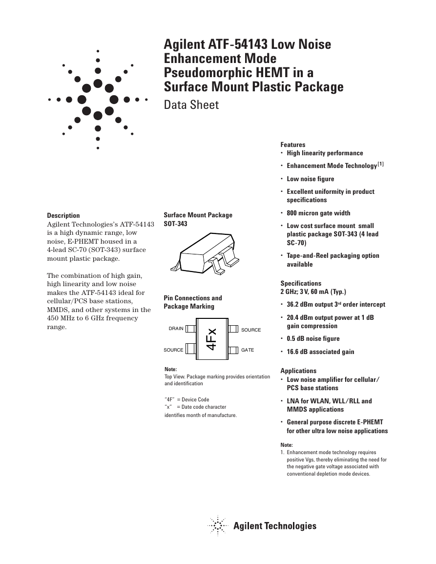
Description
Agilent Technologies’s ATF-54143
is a high dynamic range, low
noise, E-PHEMT housed in a
4-lead SC-70 (SOT-343) surface
mount plastic package.
The combination of high gain,
high linearity and low noise
makes the ATF-54143 ideal for
cellular/PCS base stations,
MMDS, and other systems in the
450 MHz to 6 GHz frequency
range.
Surface Mount Package
SOT-343
Pin Connections and
Package Marking
DRAIN
SOURCE
x
F
4
Note:
Top View. Package marking provides orientation
and identification
“4F” = Device Code
“x” = Date code character
identifies month of manufacture.
Applications
• Low noise amplifier for cellular/
PCS base stations
• LNA for WLAN, WLL/RLL and
MMDS applications
• General purpose discrete E-PHEMT
for other ultra low noise applications
Note:
1. Enhancement mode technology requires
positive Vgs, thereby eliminating the need for
the negative gate voltage associated with
conventional depletion mode devices.
�
Notes:
1. Operation of this device in excess of any one
of these parameters may cause permanent
damage.
2. Assumes DC quiescent conditions.
3. Source lead temperature is 25°C. Derate
6 mW/°C for TL > 92°C.
4. Thermal resistance measured using
150°C Liquid Crystal Measurement method.
5. The device can handle +10 dBm RF Input
Power provided IGS is limited to 2 mA. IGS at
P1dB drive level is bias circuit dependent. See
application section for additional information.
Units
V
V
V
mA
mW
dBm
mA
°C
°C
°C/W
Absolute
Maximum
5
-5 to 1
5
120
360
10[5]
2[5]
150
-65 to 150
162
ATF-54143 Absolute Maximum Ratings[1]
Symbol
Parameter
VDS
VGS
VGD
IDS
Pdiss
Pin max.
IGS
TCH
TSTG
θjc
120
100
80
60
40
20
)
A
m
(
S
D
I
Drain - Source Voltage[2]
Gate - Source Voltage[2]
Gate Drain Voltage [2]
Drain Current [2]
Total Power Dissipation [3]
RF Input Power
Gate Source Current
Channel Temperature
Storage Temperature
Thermal Resistance [4]
0.7V
0.6V
0.5V
0.4V
0.3V
3
4
VDS (V)
5
6
7
0
0
1
2
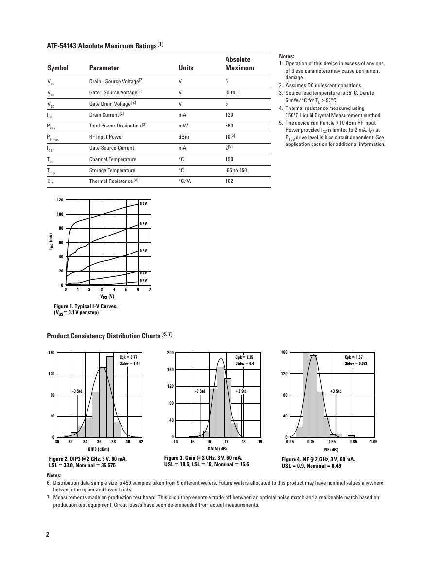
Figure 1. Typical I-V Curves.
(VGS = 0.1 V per step)
Product Consistency Distribution Charts [6, 7]
160
120
80
40
-3 Std
Cpk = 0.77
Stdev = 1.41
200
160
120
80
40
0
30
32
34
36
38
40
42
0
14
15
Cpk = 1.35
Stdev = 0.4
-3 Std
+3 Std
16
17
GAIN (dB)
18
19
Cpk = 1.67
Stdev = 0.073
+3 Std
160
120
80
40
0
0.25
0.45
0.65
0.85
1.05
NF (dB)
Figure 4. NF @ 2 GHz, 3 V, 60 mA.
USL = 0.9, Nominal = 0.49
OIP3 (dBm)
Figure 2. OIP3 @ 2 GHz, 3 V, 60 mA.
LSL = 33.0, Nominal = 36.575
Figure 3. Gain @ 2 GHz, 3 V, 60 mA.
USL = 18.5, LSL = 15, Nominal = 16.6
Notes:
6. Distribution data sample size is 450 samples taken from 9 different wafers. Future wafers allocated to this product may have nominal values anywhere
between the upper and lower limits.
7. Measurements made on production test board. This circuit represents a trade-off between an optimal noise match and a realizeable match based on
production test equipment. Circut losses have been de-embeaded from actual measurements.
2
�
ATF-54143 Electrical Specifications
TA = 25°C, RF parameters measured in a test circuit for a typical device
Symbol
Parameter and Test Condition
Vgs
Vth
Idss
Gm
Igss
NF
Ga
OIP3
P1dB
Operational Gate Voltage
Threshold Voltage
Saturated Drain Current
Transconductance
Gate Leakage Current
Noise Figure [1]
Associated Gain [1]
Output 3rd Order
Intercept Point [1]
1dB Compressed
Output Power [1]
Vds = 3V, Ids = 60 mA
Vds = 3V, Ids = 4 mA
Vds = 3V, Vgs = 0V
Vds = 3V, gm = ∆Idss/∆Vgs;
∆Vgs = 0.75 - 0.7 = 0.05V
f = 2 GHz
f = 900 MHz
f = 2 GHz
f = 900 MHz
f = 2 GHz
f = 900 MHz
f = 2 GHz
f = 900 MHz
Vgd = Vgs = -3V
Vds = 3V, Ids = 60 mA
Vds = 3V, Ids = 60 mA
Vds = 3V, Ids = 60 mA
Vds = 3V, Ids = 60 mA
Vds = 3V, Ids = 60 mA
Vds = 3V, Ids = 60 mA
Vds = 3V, Ids = 60 mA
Vds = 3V, Ids = 60 mA
Notes:
1. Measurements obtained using production test board described in Figure 5.
2. Typical values measured from a sample size of 450 parts from 9 wafers.
Units
Min.
Typ.[2]
Max.
V
V
µA
mmho
µA
dB
dB
dB
dB
dBm
dBm
dBm
dBm
0.4
0.18
—
230
—
—
—
15
—
33
—
—
—
0.59
0.38
1
410
—
0.5
0.3
16.6
23.4
36.2
35.5
20.4
18.4
0.75
0.52
5
560
200
0.9
—
18.5
—
—
—
—
—
Input
50 Ohm
Transmission
Line Including
Gate Bias T
(0.3 dB loss)
Input
Matching Circuit
Γ_mag = 0.30
Γ_ang = 150°
(0.3 dB loss)
DUT
Output
Matching Circuit
Γ_mag = 0.035
Γ_ang = -71°
(0.4 dB loss)
50 Ohm
Transmission
Line Including
Drain Bias T
(0.3 dB loss)
Output
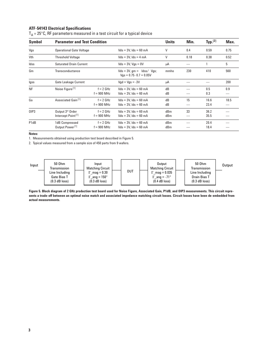
Figure 5. Block diagram of 2 GHz production test board used for Noise Figure, Associated Gain, P1dB, and OIP3 measurements. This circuit repre-
sents a trade-off between an optimal noise match and associated impedance matching circuit losses. Circuit losses have been de-embedded from
actual measurements.
3
�
ATF-54143 Typical Performance Curves
0.7
0.6
0.5
0.4
0.3
)
B
d
(
n
i
m
F
0.6
0.5
0.4
0.3
0.2
0.1
)
B
d
(
n
i
m
F
3V
4V
3V
4V
0.2
0
20
60
40
Id (mA)
80
100
0
0
20
60
40
Id (mA)
80
100
)
B
d
(
N
A
G
I
19
18
17
16
15
14
13
12
3V
4V
80
100
0
20
60
40
Ids (mA)
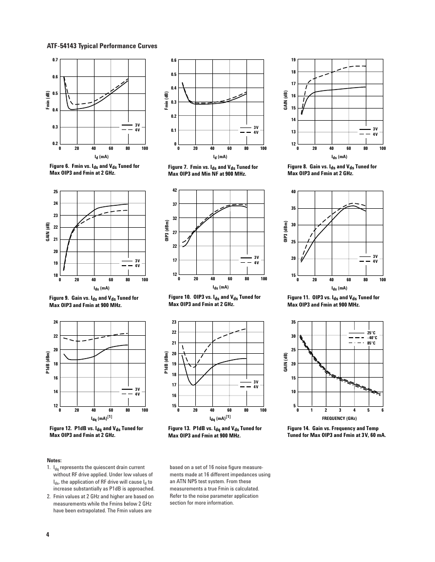
Figure 6. Fmin vs. Ids and Vds Tuned for
Max OIP3 and Fmin at 2 GHz.
Figure 7. Fmin vs. Ids and Vds Tuned for
Max OIP3 and Min NF at 900 MHz.
Figure 8. Gain vs. Ids and Vds Tuned for
Max OIP3 and Fmin at 2 GHz.
)
B
d
(
N
A
G
I
25
24
23
22
21
20
19
18
3V
4V
80
100
0
20
60
40
Ids (mA)
)
m
B
d
(
3
P
I
O
42
37
32
27
22
17
12
40
35
30
25
20
)
m
B
d
(
3
P
I
O
3V
4V
3V
4V
0
20
60
40
Ids (mA)
80
100
15
0
20
60
40
Ids (mA)
80
100
Figure 9. Gain vs. Ids and Vds Tuned for
Max OIP3 and Fmin at 900 MHz.
Figure 10. OIP3 vs. Ids and Vds Tuned for
Max OIP3 and Fmin at 2 GHz.
Figure 11. OIP3 vs. Ids and Vds Tuned for
Max OIP3 and Fmin at 900 MHz.
)
m
B
d
(
B
d
1
P
24
22
20
18
16
14
12
3V
4V
0
20
40
60
Idq (mA)[1]
80
100
)
m
B
d
(
B
d
1
P
23
22
21
20
19
18
17
16
15
3V
4V
0
20
40
60
Idq (mA)[1]
80
100
)
B
d
(
N
A
G
I
35
30
25
20
15
10
5
0
25°C
-40°C
85°C
1
2
3
4
5
6
FREQUENCY (GHz)
Figure 12. P1dB vs. Idq and Vds Tuned for
Max OIP3 and Fmin at 2 GHz.
Figure 13. P1dB vs. Idq and Vds Tuned for
Max OIP3 and Fmin at 900 MHz.
Figure 14. Gain vs. Frequency and Temp
Tuned for Max OIP3 and Fmin at 3V, 60 mA.
Notes:
1. Idq represents the quiescent drain current
without RF drive applied. Under low values of
Ids, the application of RF drive will cause Id to
increase substantially as P1dB is approached.
2. Fmin values at 2 GHz and higher are based on
measurements while the Fmins below 2 GHz
have been extrapolated. The Fmin values are
based on a set of 16 noise figure measure-
ments made at 16 different impedances using
an ATN NP5 test system. From these
measurements a true Fmin is calculated.
Refer to the noise parameter application
section for more information.
4
�
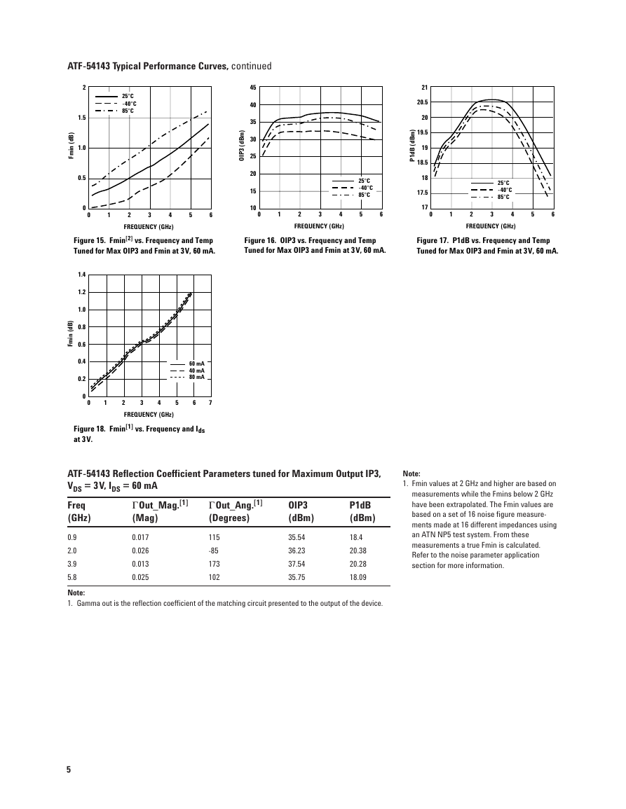
ATF-54143 Typical Performance Curves, continued
)
B
d
(
n
i
m
F
2
1.5
1.0
0.5
0
0
25°C
-40°C
85°C
1
2
3
4
5
6
FREQUENCY (GHz)
)
m
B
d
(
3
P
I
O
45
40
35
30
25
20
15
10
25°C
-40°C
85°C
0
1
2
3
4
5
6
FREQUENCY (GHz)
)
m
B
d
(
B
d
1
P
21
20.5
20
19.5
19
18.5
18
17.5
17
0
25°C
-40°C
85°C
1
2
3
4
5
6
FREQUENCY (GHz)
Figure 15. Fmin[2] vs. Frequency and Temp
Tuned for Max OIP3 and Fmin at 3V, 60 mA.
Figure 16. OIP3 vs. Frequency and Temp
Tuned for Max OIP3 and Fmin at 3V, 60 mA.
Figure 17. P1dB vs. Frequency and Temp
Tuned for Max OIP3 and Fmin at 3V, 60 mA.
)
B
d
(
n
i
m
F
1.4
1.2
1.0
0.8
0.6
0.4
0.2
0
0
60 mA
40 mA
80 mA
1
2
3
4
5
6
7
FREQUENCY (GHz)
Figure 18. Fmin[1] vs. Frequency and Ids
at 3V.
Note:
1. Fmin values at 2 GHz and higher are based on
measurements while the Fmins below 2 GHz
have been extrapolated. The Fmin values are
based on a set of 16 noise figure measure-
ments made at 16 different impedances using
an ATN NP5 test system. From these
measurements a true Fmin is calculated.
Refer to the noise parameter application
section for more information.
ATF-54143 Reflection Coefficient Parameters tuned for Maximum Output IP3,
VDS = 3V, IDS = 60 mA
Freq
(GHz)
ΓOut_Mag.[1]
(Mag)
P1dB
(dBm)
ΓOut_Ang.[1]
(Degrees)
OIP3
(dBm)
0.9
2.0
3.9
5.8
0.017
0.026
0.013
0.025
115
-85
173
102
35.54
36.23
37.54
35.75
18.4
20.38
20.28
18.09
Note:
1. Gamma out is the reflection coefficient of the matching circuit presented to the output of the device.
5
�
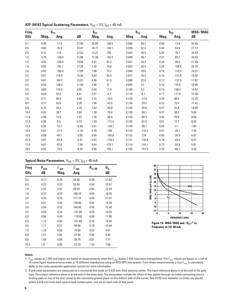
ATF-54143 Typical Scattering Parameters, VDS = 3V, IDS = 40 mA
Freq.
GHz
S21
Mag.
Mag.
S11
Ang.
Ang.
dB
0.1
0.5
0.9
1.0
1.5
1.9
2.0
2.5
3.0
4.0
5.0
6.0
7.0
8.0
9.0
10.0
11.0
12.0
13.0
14.0
15.0
16.0
17.0
18.0
0.99
0.83
0.72
0.70
0.65
0.63
0.62
0.61
0.61
0.63
0.66
0.69
0.71
0.72
0.76
0.83
0.85
0.88
0.89
0.87
0.88
0.87
0.87
0.92
-17.6
-76.9
-114
-120.6
-146.5
-162.1
-165.6
178.5
164.2
138.4
116.5
97.9
80.8
62.6
45.2
28.2
13.9
-0.5
-15.1
-31.6
-46.1
-54.8
-62.8
-73.6
27.99
25.47
22.52
21.86
19.09
17.38
17.00
15.33
13.91
11.59
9.65
8.01
6.64
5.38
4.20
2.84
1.42
0.23
-0.86
-2.18
-3.85
-5.61
-7.09
-8.34
25.09
18.77
13.37
12.39
9.01
7.40
7.08
5.84
4.96
3.80
3.04
2.51
2.15
1.86
1.62
1.39
1.18
1.03
0.91
0.78
0.64
0.52
0.44
0.38
Typical Noise Parameters, VDS = 3V, IDS = 40 mA
Freq
Rn/50
GHz
Γopt
Mag.
Γopt
Ang.
Fmin
dB
0.5
0.9
1.0
1.9
2.0
2.4
3.0
3.9
5.0
5.8
6.0
7.0
8.0
9.0
10.0
0.17
0.22
0.24
0.42
0.45
0.51
0.59
0.69
0.90
1.14
1.17
1.24
1.57
1.64
1.8
0.34
0.32
0.32
0.29
0.29
0.30
0.32
0.34
0.45
0.50
0.52
0.58
0.60
0.69
0.80
34.80
53.00
60.50
108.10
111.10
136.00
169.90
-151.60
-119.50
-101.60
-99.60
-79.50
-57.90
-39.70
-22.20
0.04
0.04
0.04
0.04
0.04
0.04
0.05
0.05
0.09
0.16
0.18
0.33
0.56
0.87
1.34
168.5
130.1
108
103.9
87.4
76.6
74.2
62.6
51.5
31
11.6
-6.7
-24.5
-42.5
-60.8
-79.8
-96.9
-112.4
-129.7
-148
-164.8
-178.4
170.1
156.1
Ga
dB
27.83
23.57
22.93
18.35
17.91
16.39
15.40
13.26
11.89
10.95
10.64
9.61
8.36
7.77
7.68
S12
Mag.
0.009
0.036
0.047
0.049
0.057
0.063
0.065
0.072
0.080
0.094
0.106
0.118
0.128
0.134
0.145
0.150
0.149
0.150
0.149
0.143
0.132
0.121
0.116
0.109
Ang.
80.2
52.4
40.4
38.7
33.3
30.4
29.8
26.6
22.9
14
4.2
-6.1
-17.6
-29.3
-40.6
-56.1
-69.3
-81.6
-95.7
-110.3
-124
-134.6
-144.1
-157.4
S22
Mag.
0.59
0.44
0.33
0.31
0.24
0.20
0.19
0.15
0.12
0.10
0.14
0.17
0.20
0.22
0.27
0.37
0.45
0.51
0.54
0.61
0.65
0.70
0.73
0.76
Ang.
-12.8
-54.6
-78.7
-83.2
-99.5
-108.6
-110.9
-122.6
-137.5
176.5
138.4
117.6
98.6
73.4
52.8
38.3
25.8
12.7
-4.1
-20.1
-34.9
-45.6
-55.9
-68.7
MSG/MAG
dB
34.45
27.17
24.54
24.03
21.99
20.70
20.37
19.09
17.92
16.06
14.57
13.28
12.25
11.42
10.48
9.66
8.98
8.35
7.84
7.36
6.87
6.37
5.81
5.46
)
B
d
(
1
2
S
d
n
a
G
A
M
/
G
S
M
40
35
30
25
20
15
10
5
0
-5
10
-15
MSG
S21
0
5
10
15
20
FREQUENCY (GHz)
Figure 19. MSG/MAG and |S21|2 vs.
Frequency at 3V, 40 mA.
Notes:
1. Fmin values at 2 GHz and higher are based on measurements while the Fmins below 2 GHz have been extrapolated. The Fmin values are based on a set of
16 noise figure measurements made at 16 different impedances using an ATN NP5 test system. From these measurements a true Fmin is calculated.
Refer to the noise parameter application section for more information.
2. S and noise parameters are measured on a microstrip line made on 0.025 inch thick alumina carrier. The input reference plane is at the end of the gate
lead. The output reference plane is at the end of the drain lead. The parameters include the effect of four plated through via holes connecting source
landing pads on top of the test carrier to the microstrip ground plane on the bottom side of the carrier. Two 0.020 inch diameter via holes are placed
within 0.010 inch from each source lead contact point, one via on each side of that point.
6
�
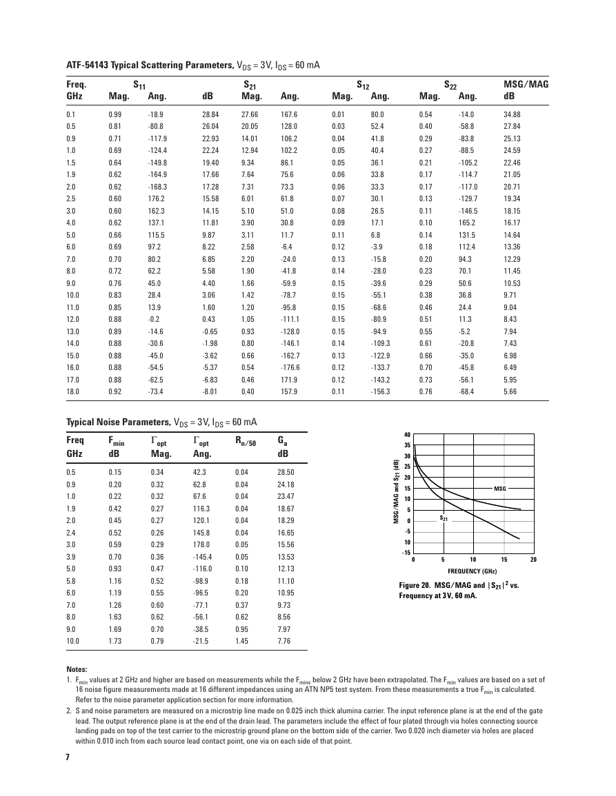
ATF-54143 Typical Scattering Parameters, VDS = 3V, IDS = 60 mA
Freq.
GHz
S21
Mag.
Mag.
S11
Ang.
Ang.
dB
0.1
0.5
0.9
1.0
1.5
1.9
2.0
2.5
3.0
4.0
5.0
6.0
7.0
8.0
9.0
10.0
11.0
12.0
13.0
14.0
15.0
16.0
17.0
18.0
0.99
0.81
0.71
0.69
0.64
0.62
0.62
0.60
0.60
0.62
0.66
0.69
0.70
0.72
0.76
0.83
0.85
0.88
0.89
0.88
0.88
0.88
0.88
0.92
-18.9
-80.8
-117.9
-124.4
-149.8
-164.9
-168.3
176.2
162.3
137.1
115.5
97.2
80.2
62.2
45.0
28.4
13.9
-0.2
-14.6
-30.6
-45.0
-54.5
-62.5
-73.4
28.84
26.04
22.93
22.24
19.40
17.66
17.28
15.58
14.15
11.81
9.87
8.22
6.85
5.58
4.40
3.06
1.60
0.43
-0.65
-1.98
-3.62
-5.37
-6.83
-8.01
27.66
20.05
14.01
12.94
9.34
7.64
7.31
6.01
5.10
3.90
3.11
2.58
2.20
1.90
1.66
1.42
1.20
1.05
0.93
0.80
0.66
0.54
0.46
0.40
Typical Noise Parameters, VDS = 3V, IDS = 60 mA
Freq
Rn/50
GHz
Γopt
Mag.
Γopt
Ang.
Fmin
dB
0.5
0.9
1.0
1.9
2.0
2.4
3.0
3.9
5.0
5.8
6.0
7.0
8.0
9.0
10.0
0.15
0.20
0.22
0.42
0.45
0.52
0.59
0.70
0.93
1.16
1.19
1.26
1.63
1.69
1.73
0.34
0.32
0.32
0.27
0.27
0.26
0.29
0.36
0.47
0.52
0.55
0.60
0.62
0.70
0.79
42.3
62.8
67.6
116.3
120.1
145.8
178.0
-145.4
-116.0
-98.9
-96.5
-77.1
-56.1
-38.5
-21.5
0.04
0.04
0.04
0.04
0.04
0.04
0.05
0.05
0.10
0.18
0.20
0.37
0.62
0.95
1.45
167.6
128.0
106.2
102.2
86.1
75.6
73.3
61.8
51.0
30.8
11.7
-6.4
-24.0
-41.8
-59.9
-78.7
-95.8
-111.1
-128.0
-146.1
-162.7
-176.6
171.9
157.9
Ga
dB
28.50
24.18
23.47
18.67
18.29
16.65
15.56
13.53
12.13
11.10
10.95
9.73
8.56
7.97
7.76
S12
Mag.
0.01
0.03
0.04
0.05
0.05
0.06
0.06
0.07
0.08
0.09
0.11
0.12
0.13
0.14
0.15
0.15
0.15
0.15
0.15
0.14
0.13
0.12
0.12
0.11
Ang.
80.0
52.4
41.8
40.4
36.1
33.8
33.3
30.1
26.5
17.1
6.8
-3.9
-15.8
-28.0
-39.6
-55.1
-68.6
-80.9
-94.9
-109.3
-122.9
-133.7
-143.2
-156.3
S22
Mag.
0.54
0.40
0.29
0.27
0.21
0.17
0.17
0.13
0.11
0.10
0.14
0.18
0.20
0.23
0.29
0.38
0.46
0.51
0.55
0.61
0.66
0.70
0.73
0.76
Ang.
-14.0
-58.8
-83.8
-88.5
-105.2
-114.7
-117.0
-129.7
-146.5
165.2
131.5
112.4
94.3
70.1
50.6
36.8
24.4
11.3
-5.2
-20.8
-35.0
-45.8
-56.1
-68.4
MSG/MAG
dB
34.88
27.84
25.13
24.59
22.46
21.05
20.71
19.34
18.15
16.17
14.64
13.36
12.29
11.45
10.53
9.71
9.04
8.43
7.94
7.43
6.98
6.49
5.95
5.66
)
B
d
(
1
2
S
d
n
a
G
A
M
/
G
S
M
40
35
30
25
20
15
10
5
0
-5
10
-15
MSG
S21
0
5
10
15
20
FREQUENCY (GHz)
Figure 20. MSG/MAG and |S21|2 vs.
Frequency at 3V, 60 mA.
Notes:
1. Fmin values at 2 GHz and higher are based on measurements while the Fmins below 2 GHz have been extrapolated. The Fmin values are based on a set of
16 noise figure measurements made at 16 different impedances using an ATN NP5 test system. From these measurements a true Fmin is calculated.
Refer to the noise parameter application section for more information.
2. S and noise parameters are measured on a microstrip line made on 0.025 inch thick alumina carrier. The input reference plane is at the end of the gate
lead. The output reference plane is at the end of the drain lead. The parameters include the effect of four plated through via holes connecting source
landing pads on top of the test carrier to the microstrip ground plane on the bottom side of the carrier. Two 0.020 inch diameter via holes are placed
within 0.010 inch from each source lead contact point, one via on each side of that point.
7
�
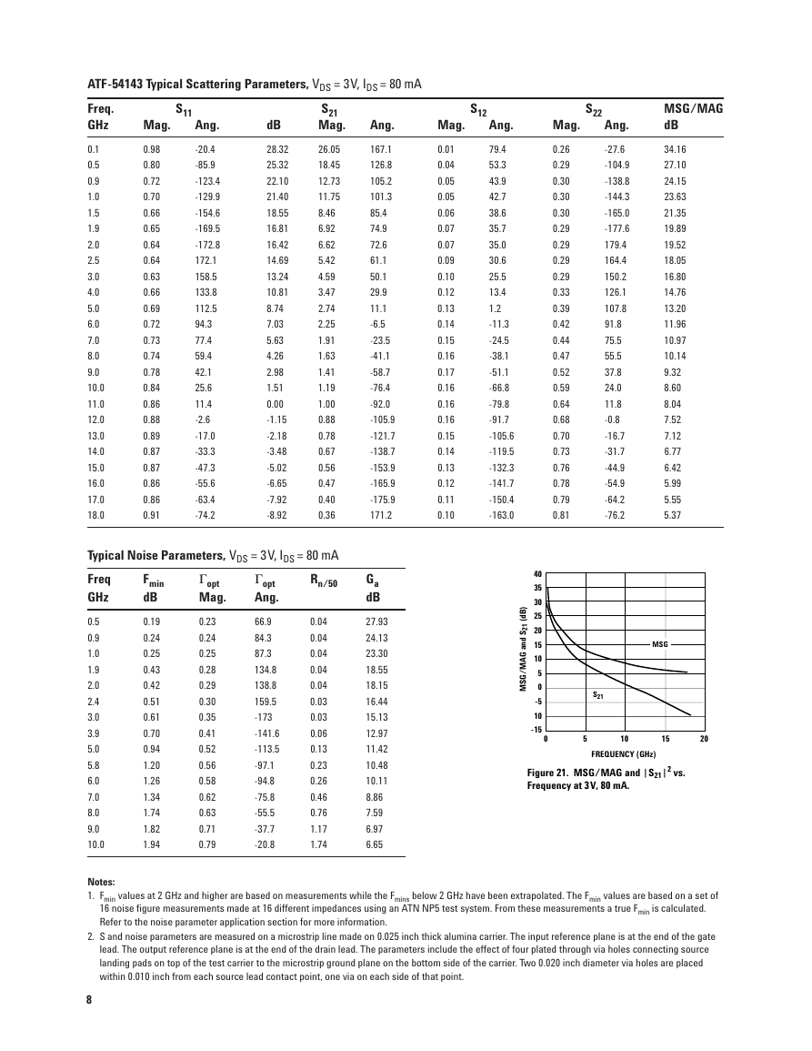
ATF-54143 Typical Scattering Parameters, VDS = 3V, IDS = 80 mA
Freq.
GHz
S21
Mag.
Mag.
S11
Ang.
Ang.
dB
0.1
0.5
0.9
1.0
1.5
1.9
2.0
2.5
3.0
4.0
5.0
6.0
7.0
8.0
9.0
10.0
11.0
12.0
13.0
14.0
15.0
16.0
17.0
18.0
0.98
0.80
0.72
0.70
0.66
0.65
0.64
0.64
0.63
0.66
0.69
0.72
0.73
0.74
0.78
0.84
0.86
0.88
0.89
0.87
0.87
0.86
0.86
0.91
-20.4
-85.9
-123.4
-129.9
-154.6
-169.5
-172.8
172.1
158.5
133.8
112.5
94.3
77.4
59.4
42.1
25.6
11.4
-2.6
-17.0
-33.3
-47.3
-55.6
-63.4
-74.2
28.32
25.32
22.10
21.40
18.55
16.81
16.42
14.69
13.24
10.81
8.74
7.03
5.63
4.26
2.98
1.51
0.00
-1.15
-2.18
-3.48
-5.02
-6.65
-7.92
-8.92
26.05
18.45
12.73
11.75
8.46
6.92
6.62
5.42
4.59
3.47
2.74
2.25
1.91
1.63
1.41
1.19
1.00
0.88
0.78
0.67
0.56
0.47
0.40
0.36
Typical Noise Parameters, VDS = 3V, IDS = 80 mA
Freq
Rn/50
GHz
Γopt
Mag.
Γopt
Ang.
Fmin
dB
0.5
0.9
1.0
1.9
2.0
2.4
3.0
3.9
5.0
5.8
6.0
7.0
8.0
9.0
10.0
0.19
0.24
0.25
0.43
0.42
0.51
0.61
0.70
0.94
1.20
1.26
1.34
1.74
1.82
1.94
0.23
0.24
0.25
0.28
0.29
0.30
0.35
0.41
0.52
0.56
0.58
0.62
0.63
0.71
0.79
66.9
84.3
87.3
134.8
138.8
159.5
-173
-141.6
-113.5
-97.1
-94.8
-75.8
-55.5
-37.7
-20.8
0.04
0.04
0.04
0.04
0.04
0.03
0.03
0.06
0.13
0.23
0.26
0.46
0.76
1.17
1.74
167.1
126.8
105.2
101.3
85.4
74.9
72.6
61.1
50.1
29.9
11.1
-6.5
-23.5
-41.1
-58.7
-76.4
-92.0
-105.9
-121.7
-138.7
-153.9
-165.9
-175.9
171.2
Ga
dB
27.93
24.13
23.30
18.55
18.15
16.44
15.13
12.97
11.42
10.48
10.11
8.86
7.59
6.97
6.65
S12
Mag.
0.01
0.04
0.05
0.05
0.06
0.07
0.07
0.09
0.10
0.12
0.13
0.14
0.15
0.16
0.17
0.16
0.16
0.16
0.15
0.14
0.13
0.12
0.11
0.10
Ang.
79.4
53.3
43.9
42.7
38.6
35.7
35.0
30.6
25.5
13.4
1.2
-11.3
-24.5
-38.1
-51.1
-66.8
-79.8
-91.7
-105.6
-119.5
-132.3
-141.7
-150.4
-163.0
S22
Mag.
0.26
0.29
0.30
0.30
0.30
0.29
0.29
0.29
0.29
0.33
0.39
0.42
0.44
0.47
0.52
0.59
0.64
0.68
0.70
0.73
0.76
0.78
0.79
0.81
Ang.
-27.6
-104.9
-138.8
-144.3
-165.0
-177.6
179.4
164.4
150.2
126.1
107.8
91.8
75.5
55.5
37.8
24.0
11.8
-0.8
-16.7
-31.7
-44.9
-54.9
-64.2
-76.2
MSG/MAG
dB
34.16
27.10
24.15
23.63
21.35
19.89
19.52
18.05
16.80
14.76
13.20
11.96
10.97
10.14
9.32
8.60
8.04
7.52
7.12
6.77
6.42
5.99
5.55
5.37
)
B
d
(
1
2
S
d
n
a
G
A
M
/
G
S
M
40
35
30
25
20
15
10
5
0
-5
10
-15
MSG
S21
0
5
10
15
20
FREQUENCY (GHz)
Figure 21. MSG/MAG and |S21|2 vs.
Frequency at 3V, 80 mA.
Notes:
1. Fmin values at 2 GHz and higher are based on measurements while the Fmins below 2 GHz have been extrapolated. The Fmin values are based on a set of
16 noise figure measurements made at 16 different impedances using an ATN NP5 test system. From these measurements a true Fmin is calculated.
Refer to the noise parameter application section for more information.
2. S and noise parameters are measured on a microstrip line made on 0.025 inch thick alumina carrier. The input reference plane is at the end of the gate
lead. The output reference plane is at the end of the drain lead. The parameters include the effect of four plated through via holes connecting source
landing pads on top of the test carrier to the microstrip ground plane on the bottom side of the carrier. Two 0.020 inch diameter via holes are placed
within 0.010 inch from each source lead contact point, one via on each side of that point.
8
�


 2023年江西萍乡中考道德与法治真题及答案.doc
 2012年重庆南川中考生物真题及答案.doc
 2013年江西师范大学地理学综合及文艺理论基础考研真题.doc
 2020年四川甘孜小升初语文真题及答案I卷.doc
 2020年注册岩土工程师专业基础考试真题及答案.doc
 2023-2024学年福建省厦门市九年级上学期数学月考试题及答案.doc
 2021-2022学年辽宁省沈阳市大东区九年级上学期语文期末试题及答案.doc
 2022-2023学年北京东城区初三第一学期物理期末试卷及答案.doc
 2018上半年江西教师资格初中地理学科知识与教学能力真题及答案.doc
 2012年河北国家公务员申论考试真题及答案-省级.doc
 2020-2021学年江苏省扬州市江都区邵樊片九年级上学期数学第一次质量检测试题及答案.doc
 2022下半年黑龙江教师资格证中学综合素质真题及答案.doc