logo资料库

mipi DPHY2.0 spec.pdf

第1页 / 共143页
第2页 / 共143页
第3页 / 共143页
第4页 / 共143页
第5页 / 共143页
第6页 / 共143页
第7页 / 共143页
第8页 / 共143页
资料共143页,剩余部分请下载后查看
Contents
Figures
Tables
Release History
1 Introduction
1.1 Scope
1.2 Purpose
2 Terminology
2.1 Use of Special Terms
2.2 Definitions
2.3 Abbreviations
2.4 Acronyms
3 References
4 D-PHY Overview
4.1 Summary of PHY Functionality
4.2 Mandatory Functionality
5 Architecture
5.1 Lane Modules
5.2 Master and Slave
5.3 High Frequency Clock Generation
5.4 Clock Lane, Data Lanes and the PHY-Protocol Interface
5.5 Selectable Lane Options
5.6 Lane Module Types
5.6.1 Unidirectional Data Lane
5.6.2 Bi-directional Data Lanes
5.6.2.1 Bi-directional Data Lane without High-Speed Reverse Communication
5.6.2.2 Bi-directional Data Lane with High-Speed Reverse Communication
5.6.3 Clock Lane
5.7 Configurations
5.7.1 Unidirectional Configurations
5.7.1.1 PHY Configuration with a Single Data Lane
5.7.1.2 PHY Configuration with Multiple Data Lanes
5.7.1.3 Dual-Simplex (Two Directions with Unidirectional Lanes)
5.7.2 Bi-Directional Half-Duplex Configurations
5.7.2.1 PHY Configurations with a Single Data Lane
5.7.2.2 PHY Configurations with Multiple Data Lanes
5.7.3 Mixed Data Lane Configurations
6 Global Operation
6.1 Transmission Data Structure
6.1.1 Data Units
6.1.2 Bit order, Serialization, and De-Serialization
6.1.3 Encoding and Decoding
6.1.4 Data Buffering
6.2 Lane States and Line Levels
6.3 Operating Modes: Control, High-Speed, and Escape
6.4 High-Speed Data Transmission
6.4.1 Burst Payload Data
6.4.2 Start-of-Transmission
6.4.3 End-of-Transmission
6.4.4 HS Data Transmission Burst
6.5 Bi-directional Data Lane Turnaround
6.6 Escape Mode
6.6.1 Remote Triggers
6.6.2 Low-Power Data Transmission
6.6.3 Ultra-Low Power State
6.6.4 Escape Mode State Machine
6.7 High-Speed Clock Transmission
6.8 Clock Lane Ultra-Low Power State
6.9 Global Operation Timing Parameters
6.10 System Power States
6.11 Initialization
6.12 Calibration
6.13 Global Operation Flow Diagram
6.14 Data Rate Dependent Parameters (informative)
6.14.1 Parameters Containing Only UI Values
6.14.2 Parameters Containing Time and UI values
6.14.3 Parameters Containing Only Time Values
6.14.4 Parameters Containing Only Time Values That Are Not Data Rate Dependent
6.15 Interoperability
7 Fault Detection
7.1 Contention Detection
7.2 Sequence Error Detection
7.2.1 SoT Error
7.2.2 SoT Sync Error
7.2.3 EoT Sync Error
7.2.4 Escape Mode Entry Command Error
7.2.5 LP Transmission Sync Error
7.2.6 False Control Error
7.3 Protocol Watchdog Timers (informative)
7.3.1 HS RX Timeout
7.3.2 HS TX Timeout
7.3.3 Escape Mode Timeout
7.3.4 Escape Mode Silence Timeout
7.3.5 Turnaround Errors
8 Interconnect and Lane Configuration
8.1 Lane Configuration
8.2 Boundary Conditions
8.3 Definitions
8.4 S-parameter Specifications
8.5 Characterization Conditions
8.6 Interconnect Specifications
8.6.1 Differential Characteristics
8.6.1.1 Differential Insertion Loss for Data Rate ≥ 80 Mbps and ≤ 1.5 Gbps
8.6.1.2 Differential Insertion Loss for Data Rate > 1.5 Gbps and ≤ 4.5 Gbps
8.6.1.3 Differential Reflection Loss for Data Rate ≥ 80 Mbps and ≤ 1.5 Gbps
8.6.1.4 Differential Reflection Loss for Data Rate >1.5 Gbps and ≤ 4.5 Gbps
8.6.2 Common-mode Characteristics
8.6.3 Intra-Lane Cross-Coupling
8.6.4 Mode-Conversion Limits
8.6.5 Inter-Lane Cross-Coupling
8.6.6 Inter-Lane Static Skew
8.7 Driver and Receiver Characteristics
8.7.1 Differential Characteristics
8.7.2 Common-Mode Characteristics
8.7.3 Mode-Conversion Limits
9 Electrical Characteristics
9.1 Driver Characteristics
9.1.1 High-Speed Transmitter
9.1.1.1 Differential & Common Mode Swing
9.1.1.2 Differential Voltage Mismatch
9.1.1.3 Static Common Mode Mismatch & Transient Common Mode Voltage
9.1.1.4 Output Resistance
9.1.1.5 Rise/Fall Times
9.1.1.6 Half Swing Mode
9.1.1.7 De-emphasis
9.1.2 Low-Power Transmitter
9.2 Receiver Characteristics
9.2.1 High-Speed Receiver
9.2.2 Low-Power Receiver
9.3 Line Contention Detection
9.4 Input Characteristics
10 High-Speed Data-Clock Timing
10.1 High-Speed Clock Timing
10.2 Forward High-Speed Data Transmission Timing
10.2.1 Data-Clock Timing Specifications
10.2.1.1 Data Rate ≥ 0.08 Gbps and ≤ 1 Gbps
10.2.1.2 Data Rate > 1 Gbps and ≤ 1.5 Gbps
10.2.1.3 Data Rate > 1.5 Gbps and ≤ 4.5 Gbps
10.2.2 Normative Spread Spectrum Clocking (SSC)
10.2.3 Transmitter Eye Diagram Specification
10.2.4 Receiver Eye Diagram Specification
10.3 Reverse High-Speed Data Transmission Timing
10.4 Operating Modes: Data rate and Channel Support Guidance
11 Regulatory Requirements
12 Built-In HS Test Mode (Informative)
12.1 Introduction
12.2 Entering the HS Test Mode
12.3 HS Test Mode
12.4 Special Case: Multi-Lane Testing
12.5 Exiting from HS Test Mode
Annex A Logical PHY-Protocol Interface Description (informative)
A.1 Signal Description
A.2 High-Speed Transmit from the Master Side
A.3 High-Speed Receive at the Slave Side
A.4 High-Speed Transmit from the Slave Side
A.5 High-Speed Receive at the Master Side
A.6 Low-Power Data Transmission
A.7 Low-Power Data Reception
A.8 Turn-around
A.9 Calibration
A.10 Optical Link Support
A.10.1 System Setup
A.10.2 Serializer and De-Serializer Block Diagrams
A.10.3 Timing Constraints
A.10.4 System Constraints
A.10.4.1 Bus Turnaround
A.10.4.2 Equalization (De-emphasis), Deskewing, and Spread Spectrum Clocking
A.10.4.3 TWAIT-OPTICAL
Annex B Interconnect Design Guidelines (informative)
B.1 Practical Distances
B.2 RF Frequency Bands: Interference
B.3 Transmission Line Design
B.4 Reference Layer
B.5 Printed-Circuit Board
B.6 Flex-foils
B.7 Series Resistance
B.8 Connectors
Annex C 8b9b Line Coding for D-PHY (normative)
C.1 Line Coding Features
C.1.1 Enabled Features for the Protocol
C.1.2 Enabled Features for the PHY
C.2 Coding Scheme
C.2.1 8b9b Coding Properties
C.2.2 Data Codes: Basic Code Set
C.2.3 Comma Codes: Unique Exception Codes
C.2.4 Control Codes: Regular Exception Codes
C.2.5 Complete Coding Scheme
C.3 Operation with the D-PHY
C.3.1 Payload: Data and Control
C.3.1.1 Idle/Sync Comma Symbols
C.3.1.2 Protocol Marker Comma Symbol
C.3.1.3 EoT Marker
C.3.2 Details for HS Transmission
C.3.2.1 SoT
C.3.2.2 HS Transmission Payload
C.3.2.3 EoT
C.3.3 Details for LP Transmission
C.3.3.1 SoT
C.3.3.2 LP Transmission Payload
C.3.3.3 EoT
C.4 Error Signaling
C.5 Extended PPI
C.6 Complete Code Set
Participants
Specification for D-PHYSM Version 2.0 23 November 2015 MIPI Board Adopted 08 March 2016 Further technical changes to this document are expected as work continues in the Phy Working Group. Copyright © 2007-2016 MIPI Alliance, Inc. All rights reserved. Confidential
Specification for D-PHY Version 2.0 23-Nov-2015 NOTICE OF DISCLAIMER The material contained herein is not a license, either expressly or impliedly, to any IPR owned or controlled by any of the authors or developers of this material or MIPI®. The material contained herein is provided on an “AS IS” basis and to the maximum extent permitted by applicable law, this material is provided AS IS AND WITH ALL FAULTS, and the authors and developers of this material and MIPI hereby disclaim all other warranties and conditions, either express, implied or statutory, including, but not limited to, any (if any) implied warranties, duties or conditions of merchantability, of fitness for a particular purpose, of accuracy or completeness of responses, of results, of workmanlike effort, of lack of viruses, and of lack of negligence. All materials contained herein are protected by copyright laws, and may not be reproduced, republished, distributed, transmitted, displayed, broadcast or otherwise exploited in any manner without the express prior written permission of MIPI Alliance. MIPI, MIPI Alliance and the dotted rainbow arch and all related trademarks, tradenames, and other intellectual property are the exclusive property of MIPI Alliance and cannot be used without its express prior written permission. ALSO, THERE IS NO WARRANTY OF CONDITION OF TITLE, QUIET ENJOYMENT, QUIET POSSESSION, CORRESPONDENCE TO DESCRIPTION OR NON-INFRINGEMENT WITH REGARD TO THIS MATERIAL OR THE CONTENTS OF THIS DOCUMENT. IN NO EVENT WILL ANY AUTHOR OR DEVELOPER OF THIS MATERIAL OR THE CONTENTS OF THIS DOCUMENT OR MIPI BE LIABLE TO ANY OTHER PARTY FOR THE COST OF PROCURING SUBSTITUTE GOODS OR SERVICES, LOST PROFITS, LOSS OF USE, LOSS OF DATA, OR ANY INCIDENTAL, CONSEQUENTIAL, DIRECT, INDIRECT, OR SPECIAL DAMAGES WHETHER UNDER CONTRACT, TORT, WARRANTY, OR OTHERWISE, ARISING IN ANY WAY OUT OF THIS OR ANY OTHER AGREEMENT, SPECIFICATION OR DOCUMENT RELATING TO THIS MATERIAL, WHETHER OR NOT SUCH PARTY HAD ADVANCE NOTICE OF THE POSSIBILITY OF SUCH DAMAGES. Without limiting the generality of this Disclaimer stated above, the user of the contents of this Document is further notified that MIPI: (a) does not evaluate, test or verify the accuracy, soundness or credibility of the contents of this Document; (b) does not monitor or enforce compliance with the contents of this Document; and (c) does not certify, test, or in any manner investigate products or services or any claims of compliance with the contents of this Document. The use or implementation of the contents of this Document may involve or require the use of intellectual property rights (“IPR”) including (but not limited to) patents, patent applications, or copyrights owned by one or more parties, whether or not Members of MIPI. MIPI does not make any search or investigation for IPR, nor does MIPI require or request the disclosure of any IPR or claims of IPR as respects the contents of this Document or otherwise. Questions pertaining to this document, or the terms or conditions of its provision, should be addressed to: MIPI Alliance, Inc. c/o IEEE-ISTO 445 Hoes Lane Piscataway, NJ 08854 Attn: Board Secretary ii Copyright © 2007-2016 MIPI Alliance, Inc. All rights reserved. Confidential
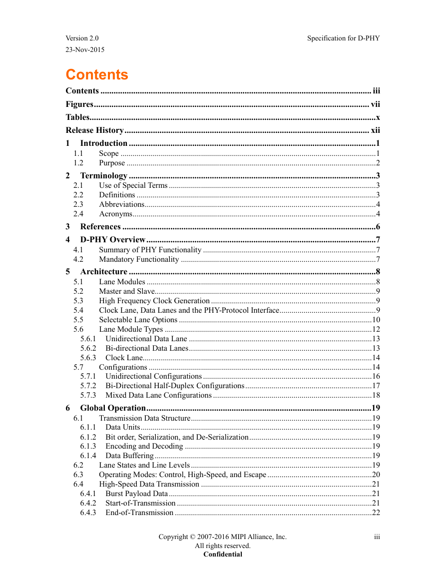
Version 2.0 23-Nov-2015 Specification for D-PHY 1.1 1.2 2.1 2.2 2.3 2.4 Contents Contents ............................................................................................................................ iii Figures .............................................................................................................................. vii Tables ...................................................................................................................................x Release History ................................................................................................................ xii Introduction .................................................................................................................1 1 Scope ............................................................................................................................... 1 Purpose ............................................................................................................................ 2 2 Terminology .................................................................................................................3 Use of Special Terms ....................................................................................................... 3 Definitions ....................................................................................................................... 3 Abbreviations ................................................................................................................... 4 Acronyms ......................................................................................................................... 4 3 References ....................................................................................................................6 4 D-PHY Overview .........................................................................................................7 4.1 Summary of PHY Functionality ...................................................................................... 7 4.2 Mandatory Functionality ................................................................................................. 7 5 Architecture .................................................................................................................8 5.1 Lane Modules .................................................................................................................. 8 5.2 Master and Slave .............................................................................................................. 9 High Frequency Clock Generation .................................................................................. 9 5.3 5.4 Clock Lane, Data Lanes and the PHY-Protocol Interface ................................................ 9 Selectable Lane Options ................................................................................................ 10 5.5 Lane Module Types ....................................................................................................... 12 5.6 5.6.1 Unidirectional Data Lane ........................................................................................... 13 5.6.2 Bi-directional Data Lanes ........................................................................................... 13 5.6.3 Clock Lane.................................................................................................................. 14 Configurations ............................................................................................................... 14 5.7.1 Unidirectional Configurations .................................................................................... 16 5.7.2 Bi-Directional Half-Duplex Configurations ............................................................... 17 5.7.3 Mixed Data Lane Configurations ............................................................................... 18 6 Global Operation .......................................................................................................19 Transmission Data Structure .......................................................................................... 19 6.1.1 Data Units ................................................................................................................... 19 6.1.2 Bit order, Serialization, and De-Serialization ............................................................. 19 6.1.3 Encoding and Decoding ............................................................................................. 19 6.1.4 Data Buffering ............................................................................................................ 19 Lane States and Line Levels .......................................................................................... 19 Operating Modes: Control, High-Speed, and Escape .................................................... 20 High-Speed Data Transmission ..................................................................................... 21 6.4.1 Burst Payload Data ..................................................................................................... 21 6.4.2 Start-of-Transmission ................................................................................................. 21 6.4.3 End-of-Transmission .................................................................................................. 22 6.2 6.3 6.4 5.7 6.1 Copyright © 2007-2016 MIPI Alliance, Inc. All rights reserved. Confidential iii
Specification for D-PHY Version 2.0 23-Nov-2015 6.5 6.6 6.14.1 6.14.2 6.14.3 6.14.4 6.4.4 HS Data Transmission Burst....................................................................................... 22 Bi-directional Data Lane Turnaround ............................................................................ 24 Escape Mode .................................................................................................................. 27 6.6.1 Remote Triggers ......................................................................................................... 28 6.6.2 Low-Power Data Transmission .................................................................................. 28 6.6.3 Ultra-Low Power State ............................................................................................... 29 6.6.4 Escape Mode State Machine ...................................................................................... 29 High-Speed Clock Transmission ................................................................................... 31 6.7 Clock Lane Ultra-Low Power State ............................................................................... 36 6.8 Global Operation Timing Parameters ............................................................................ 37 6.9 System Power States ...................................................................................................... 41 6.10 6.11 Initialization ................................................................................................................... 41 6.12 Calibration ..................................................................................................................... 41 6.13 Global Operation Flow Diagram ................................................................................... 45 6.14 Data Rate Dependent Parameters (informative) ............................................................ 47 Parameters Containing Only UI Values .................................................................. 48 Parameters Containing Time and UI values ........................................................... 48 Parameters Containing Only Time Values .............................................................. 48 Parameters Containing Only Time Values That Are Not Data Rate Dependent ..... 49 Interoperability .............................................................................................................. 49 7 Fault Detection ..........................................................................................................50 Contention Detection ..................................................................................................... 50 Sequence Error Detection .............................................................................................. 50 7.2.1 SoT Error .................................................................................................................... 51 7.2.2 SoT Sync Error ........................................................................................................... 51 7.2.3 EoT Sync Error ........................................................................................................... 51 7.2.4 Escape Mode Entry Command Error .......................................................................... 51 7.2.5 LP Transmission Sync Error ....................................................................................... 51 7.2.6 False Control Error ..................................................................................................... 51 Protocol Watchdog Timers (informative) ...................................................................... 51 7.3.1 HS RX Timeout .......................................................................................................... 51 7.3.2 HS TX Timeout .......................................................................................................... 51 7.3.3 Escape Mode Timeout ................................................................................................ 51 7.3.4 Escape Mode Silence Timeout ................................................................................... 51 7.3.5 Turnaround Errors ...................................................................................................... 52 Interconnect and Lane Configuration .....................................................................53 Lane Configuration ........................................................................................................ 53 Boundary Conditions ..................................................................................................... 53 Definitions ..................................................................................................................... 53 S-parameter Specifications ............................................................................................ 54 Characterization Conditions .......................................................................................... 54 Interconnect Specifications ............................................................................................ 54 8.6.1 Differential Characteristics ......................................................................................... 55 8.6.2 Common-mode Characteristics .................................................................................. 57 8.6.3 Intra-Lane Cross-Coupling ......................................................................................... 57 8.6.4 Mode-Conversion Limits ............................................................................................ 57 8.6.5 Inter-Lane Cross-Coupling ......................................................................................... 57 8.1 8.2 8.3 8.4 8.5 8.6 8 6.15 7.1 7.2 7.3 iv Copyright © 2007-2016 MIPI Alliance, Inc. All rights reserved. Confidential
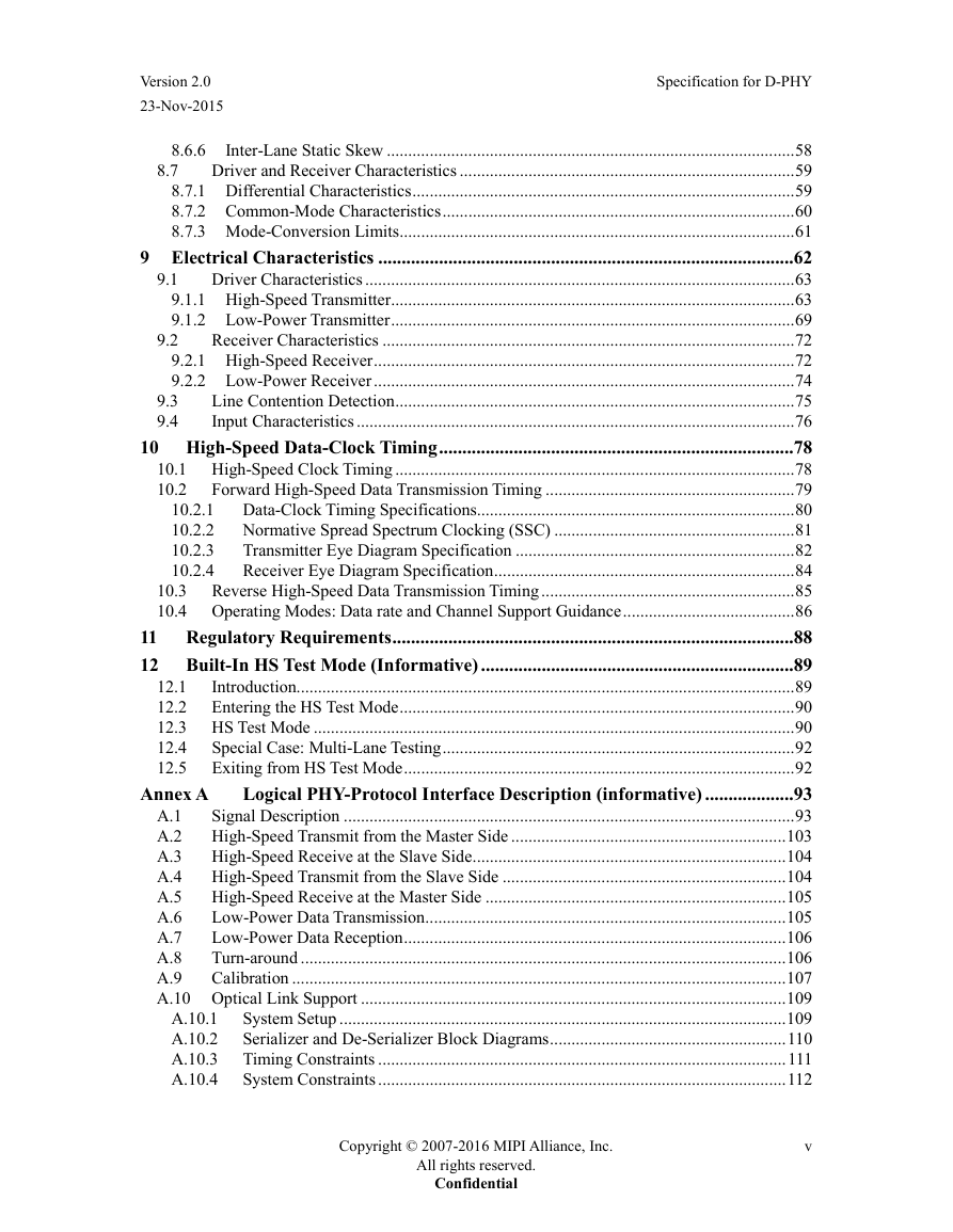
Version 2.0 23-Nov-2015 Specification for D-PHY 8.6.6 8.7 9.2 9.1 9.3 9.4 Inter-Lane Static Skew ............................................................................................... 58 Driver and Receiver Characteristics .............................................................................. 59 8.7.1 Differential Characteristics ......................................................................................... 59 8.7.2 Common-Mode Characteristics .................................................................................. 60 8.7.3 Mode-Conversion Limits ............................................................................................ 61 9 Electrical Characteristics .........................................................................................62 Driver Characteristics .................................................................................................... 63 9.1.1 High-Speed Transmitter .............................................................................................. 63 9.1.2 Low-Power Transmitter .............................................................................................. 69 Receiver Characteristics ................................................................................................ 72 9.2.1 High-Speed Receiver .................................................................................................. 72 9.2.2 Low-Power Receiver .................................................................................................. 74 Line Contention Detection ............................................................................................. 75 Input Characteristics ...................................................................................................... 76 10 High-Speed Data-Clock Timing ............................................................................78 10.1 High-Speed Clock Timing ............................................................................................. 78 Forward High-Speed Data Transmission Timing .......................................................... 79 10.2 10.2.1 Data-Clock Timing Specifications.......................................................................... 80 10.2.2 Normative Spread Spectrum Clocking (SSC) ........................................................ 81 Transmitter Eye Diagram Specification ................................................................. 82 10.2.3 10.2.4 Receiver Eye Diagram Specification ...................................................................... 84 10.3 Reverse High-Speed Data Transmission Timing ........................................................... 85 10.4 Operating Modes: Data rate and Channel Support Guidance ........................................ 86 11 Regulatory Requirements ......................................................................................88 12 Built-In HS Test Mode (Informative) ...................................................................89 Introduction.................................................................................................................... 89 12.1 12.2 Entering the HS Test Mode ............................................................................................ 90 12.3 HS Test Mode ................................................................................................................ 90 12.4 Special Case: Multi-Lane Testing .................................................................................. 92 Exiting from HS Test Mode ........................................................................................... 92 12.5 Logical PHY-Protocol Interface Description (informative) ...................93 A.1 Signal Description ......................................................................................................... 93 A.2 High-Speed Transmit from the Master Side ................................................................ 103 A.3 High-Speed Receive at the Slave Side ......................................................................... 104 A.4 High-Speed Transmit from the Slave Side .................................................................. 104 A.5 High-Speed Receive at the Master Side ...................................................................... 105 A.6 Low-Power Data Transmission .................................................................................... 105 A.7 Low-Power Data Reception ......................................................................................... 106 A.8 Turn-around ................................................................................................................. 106 A.9 Calibration ................................................................................................................... 107 A.10 Optical Link Support ................................................................................................... 109 System Setup ........................................................................................................ 109 A.10.1 A.10.2 Serializer and De-Serializer Block Diagrams ....................................................... 110 A.10.3 Timing Constraints ............................................................................................... 111 System Constraints ............................................................................................... 112 A.10.4 Annex A Copyright © 2007-2016 MIPI Alliance, Inc. All rights reserved. Confidential v
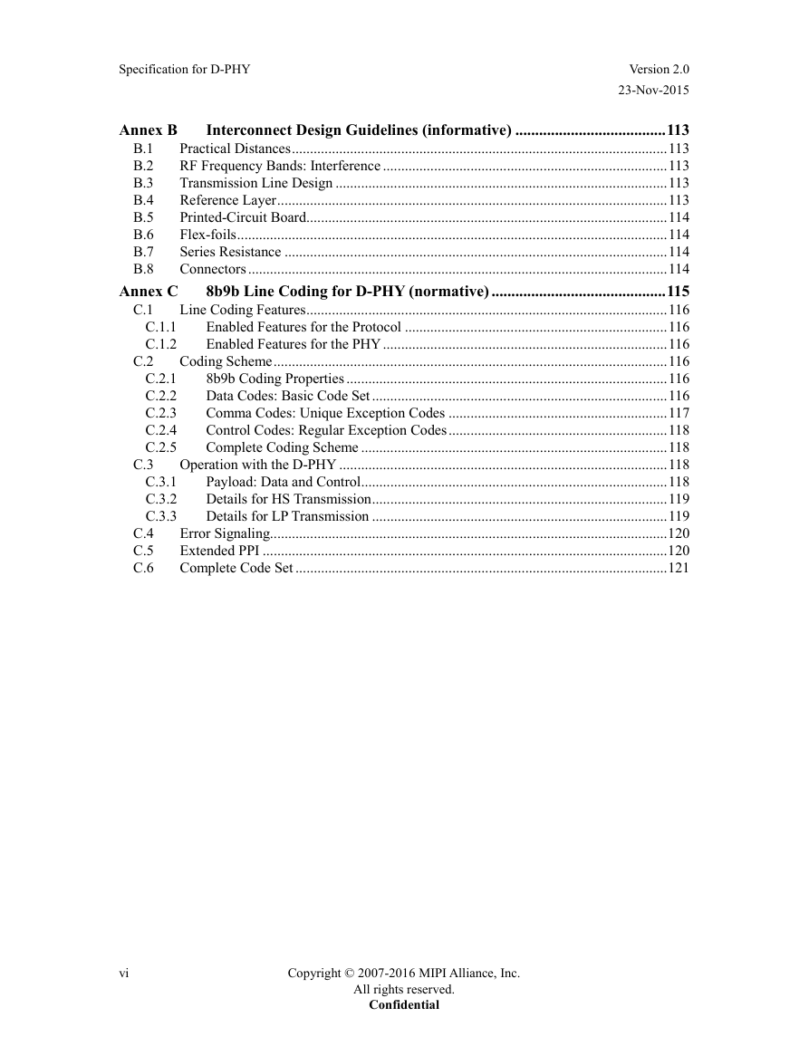
Specification for D-PHY Version 2.0 23-Nov-2015 Annex B Annex C Interconnect Design Guidelines (informative) ...................................... 113 Practical Distances ....................................................................................................... 113 RF Frequency Bands: Interference .............................................................................. 113 Transmission Line Design ........................................................................................... 113 Reference Layer ........................................................................................................... 113 Printed-Circuit Board ................................................................................................... 114 Flex-foils ...................................................................................................................... 114 Series Resistance ......................................................................................................... 114 Connectors ................................................................................................................... 114 8b9b Line Coding for D-PHY (normative) ............................................ 115 Line Coding Features ................................................................................................... 116 Enabled Features for the Protocol ........................................................................ 116 Enabled Features for the PHY .............................................................................. 116 Coding Scheme ............................................................................................................ 116 8b9b Coding Properties ........................................................................................ 116 Data Codes: Basic Code Set ................................................................................. 116 Comma Codes: Unique Exception Codes ............................................................ 117 Control Codes: Regular Exception Codes ............................................................ 118 Complete Coding Scheme .................................................................................... 118 Operation with the D-PHY .......................................................................................... 118 Payload: Data and Control .................................................................................... 118 Details for HS Transmission ................................................................................. 119 Details for LP Transmission ................................................................................. 119 Error Signaling............................................................................................................. 120 Extended PPI ............................................................................................................... 120 Complete Code Set ...................................................................................................... 121 B.1 B.2 B.3 B.4 B.5 B.6 B.7 B.8 C.1 C.2 C.1.1 C.1.2 C.2.1 C.2.2 C.2.3 C.2.4 C.2.5 C.3.1 C.3.2 C.3.3 C.3 C.4 C.5 C.6 vi Copyright © 2007-2016 MIPI Alliance, Inc. All rights reserved. Confidential
Version 2.0 23-Nov-2015 Specification for D-PHY Figures Figure 1 Universal Lane Module Functions ..................................................................................... 8 Figure 2 Two Data Lane PHY Configuration ................................................................................. 10 Figure 3 Option Selection Flow Graph .......................................................................................... 11 Figure 4 Universal Lane Module Architecture ............................................................................... 12 Figure 5 Lane Symbol Macros and Symbols Legend ..................................................................... 14 Figure 6 All Possible Data Lane Types and a Basic Unidirectional Clock Lane ............................ 15 Figure 7 Unidirectional Single Data Lane Configuration .............................................................. 16 Figure 8 Unidirectional Multiple Data Lane Configuration without LPDT ................................... 16 Figure 9 Two Directions Using Two Independent Unidirectional PHYs without LPDT ............... 17 Figure 10 Bidirectional Single Data Lane Configuration ............................................................... 17 Figure 11 Bi-directional Multiple Data Lane Configuration .......................................................... 18 Figure 12 Mixed Type Multiple Data Lane Configuration ............................................................. 18 Figure 13 Line Levels ..................................................................................................................... 20 Figure 14 High-Speed Data Transmission in Bursts ...................................................................... 22 Figure 15 TX and RX State Machines for High-Speed Data Transmission ................................... 23 Figure 16 Turnaround Procedure .................................................................................................... 25 Figure 17 Turnaround State Machine ............................................................................................. 26 Figure 18 Trigger-Reset Command in Escape Mode ..................................................................... 27 Figure 19 Two Data Byte Low-Power Data Transmission Example .............................................. 29 Figure 20 Escape Mode State Machine .......................................................................................... 30 Figure 21 Switching the Clock Lane between Clock Transmission and Low-Power Mode .......... 33 Figure 22 High-Speed Clock Transmission State Machine ............................................................ 35 Figure 23 Clock Lane Ultra-Low Power State State Machine ....................................................... 36 Figure 24 High-Speed Data Transmission in Skew-Calibration .................................................... 42 Figure 25 Normal Mode vs Skew Calibration ................................................................................ 42 Figure 26 Normal Mode vs Skew Calibration (Zoom-In) .............................................................. 43 Figure 27 Data Lane Module State Diagram .................................................................................. 46 Figure 28 Clock Lane Module State Diagram ................................................................................ 47 Figure 29 Point-to-point Interconnect ............................................................................................ 53 Figure 30 Set-up for S-parameter Characterization of RX, TX and TLIS ..................................... 54 Figure 31 Template for Differential Insertion Losses, Data Rates ≥ 80 Mbps and ≤ 1.5 Gbps ...... 55 Copyright © 2007-2016 MIPI Alliance, Inc. All rights reserved. Confidential vii
Specification for D-PHY Version 2.0 23-Nov-2015 Figure 32 Template for Differential Insertion Losses, Data Rates > 1.5 Gbps and ≤ 4.5 Gbps ..... 56 Figure 33 Template for Differential Reflection at Both Ports ........................................................ 57 Figure 34 Inter-Lane Common-mode Cross-Coupling Template ................................................... 58 Figure 35 Inter-Lane Differential Cross-Coupling Template ......................................................... 58 Figure 36 Differential Reflection Template for Lane Module Receivers ....................................... 59 Figure 37 Differential Reflection Template for Lane Module Transmitters ................................... 60 Figure 38 Template for RX Common-Mode Return Loss .............................................................. 61 Figure 39 Electrical Functions of a Fully Featured D-PHY Transceiver ....................................... 62 Figure 40 D-PHY Signaling Levels ................................................................................................ 63 Figure 41 Example HS Transmitter ................................................................................................ 64 Figure 42 Ideal Single-Ended and Resulting Differential HS Signals............................................ 65 Figure 43 Possible ΔVCMTX and ΔVOD Distortions of the Single-ended HS Signals ...................... 66 Figure 44 Example Circuit for VCMTX and VOD Measurements ................................................ 66 Figure 45 Common Mode and Differential Swing in Half Swing Mode versus Default ............... 67 Figure 46 De-emphasis Example .................................................................................................... 68 Figure 47 Example LP Transmitter ................................................................................................ 69 Figure 48 V-I Characteristic for LP Transmitter Driving Logic High ............................................ 70 Figure 49 V-I Characteristic for LP Transmitter Driving Logic Low ............................................. 70 Figure 50 LP Transmitter V-I Characteristic Measurement Setup .................................................. 70 Figure 51 HS Receiver Implementation Example .......................................................................... 73 Figure 52 Input Glitch Rejection of Low-Power Receivers ........................................................... 75 Figure 53 Signaling and Contention Voltage Levels ...................................................................... 76 Figure 54 Pin Leakage Measurement Example Circuit .................................................................. 77 Figure 55 Conceptual D-PHY Data and Clock Timing Compliance Measurement Planes ............ 78 Figure 56 DDR Clock Definition ................................................................................................... 79 Figure 57 Data to Clock Timing Definitions .................................................................................. 80 Figure 58 TX Eye Diagram Specification ...................................................................................... 83 Figure 59 Transmitter Eye Diagram Validation Setup .................................................................... 83 Figure 60 Receiver Eye Diagram Specification ............................................................................. 84 Figure 61 Receiver Eye Diagram Validation Setup ........................................................................ 85 Figure 62 Conceptual View of HS Data Transmission in Reverse Direction ................................. 85 Figure 63 Reverse High-Speed Data Transmission Timing at Slave Side...................................... 86 Figure 64 Testing with Pattern Checkers and Generators............................................................... 89 viii Copyright © 2007-2016 MIPI Alliance, Inc. All rights reserved. Confidential
分享到:
收藏