NAND FLASH MEMORY
TECHNOLOGIES
�
IEEE Press
445 Hoes Lane
Piscataway, NJ 08854
IEEE Press Editorial Board
Tariq Samad, Editor in Chief
George W. Arnold
Dmitry Goldgof
Ekram Hossain
Mary Lanzerotti
Vladimir Lumelsky
Pui-In Mak
Jeffrey Nanzer
Ray Perez
Linda Shafer
Zidong Wang
MengChu Zhou
George Zobrist
Kenneth Moore, Director of IEEE Book and Information Services (BIS)
Technical Reviewers
Joe E Brewer, PE, Electronic Engineering Consultant
Chandra Mouli, Director, R&D Device Technology, Micron Technology Inc, Boise ID, USA
Gabriel Molas, CEA LETI Minatec, Grenoble, France
�
NAND FLASH MEMORY
TECHNOLOGIES
SEIICHI ARITOME
IEEE Press Series on Microelectronic Systems
�
Copyright © 2016 by The Institute of Electrical and Electronics Engineers, Inc.
Published by John Wiley & Sons, Inc., Hoboken, New Jersey. All rights reserved
Published simultaneously in Canada
No part of this publication may be reproduced, stored in a retrieval system, or transmitted in any form or
by any means, electronic, mechanical, photocopying, recording, scanning, or otherwise, except as
permitted under Section 107 or 108 of the 1976 United States Copyright Act, without either the prior
written permission of the Publisher, or authorization through payment of the appropriate per-copy fee to
the Copyright Clearance Center, Inc., 222 Rosewood Drive, Danvers, MA 01923, (978) 750-8400, fax
(978) 750-4470, or on the web at www.copyright.com. Requests to the Publisher for permission should
be addressed to the Permissions Department, John Wiley & Sons, Inc., 111 River Street, Hoboken, NJ
07030, (201) 748-6011, fax (201) 748-6008, or online at http://www.wiley.com/go/permission.
Limit of Liability/Disclaimer of Warranty: While the publisher and author have used their best efforts in
preparing this book, they make no representations or warranties with respect to the accuracy or
completeness of the contents of this book and specifically disclaim any implied warranties of
merchantability or fitness for a particular purpose. No warranty may be created or extended by sales
representatives or written sales materials. The advice and strategies contained herein may not be suitable
for your situation. You should consult with a professional where appropriate. Neither the publisher nor
author shall be liable for any loss of profit or any other commercial damages, including but not limited to
special, incidental, consequential, or other damages.
For general information on our other products and services or for technical support, please contact our
Customer Care Department within the United States at (800) 762-2974, outside the United States at (317)
572-3993 or fax (317) 572-4002.
Wiley also publishes its books in a variety of electronic formats. Some content that appears in print may
not be available in electronic formats. For more information about Wiley products, visit our web site at
www.wiley.com.
Library of Congress Cataloging-in-Publication Data is available.
ISBN: 978-1-119-13260-8
Printed in the United States of America
10 9 8 7 6 5 4 3 2 1
�
CONTENTS
Foreword
Preface
Acknowledgments
About the Author
1
Introduction
1.1 Background, 1
1.2 Overview, 8
References, 10
2 Principle of NAND Flash Memory
2.1 NAND Flash Device and Architecture, 17
2.1.1 NAND Flash Memory Cell Architecture, 17
2.1.2 Peripheral Device, 19
2.2 Cell Operation, 21
2.2.1 Read Operation, 21
2.2.2 Program and Erase Operation, 21
2.2.3 Program and Erase Dynamics, 28
2.2.4 Program Boosting Operation, 31
2.3 Multilevel Cell (MLC), 34
2.3.1 Cell Vt Setting, 34
References, 35
xi
xv
xvii
xix
1
17
v
�
vi
CONTENTS
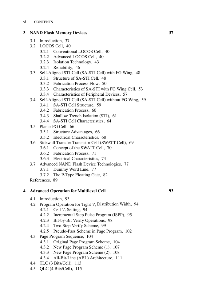
3 NAND Flash Memory Devices
37
3.1 Introduction, 37
3.2 LOCOS Cell, 40
3.2.1 Conventional LOCOS Cell, 40
3.2.2 Advanced LOCOS Cell, 40
3.2.3 Isolation Technology, 43
3.2.4 Reliability, 46
3.3 Self-Aligned STI Cell (SA-STI Cell) with FG Wing, 48
3.3.1 Structure of SA-STI Cell, 48
3.3.2 Fabrication Process Flow, 50
3.3.3 Characteristics of SA-STI with FG Wing Cell, 53
3.3.4 Characteristics of Peripheral Devices, 57
3.4 Self-Aligned STI Cell (SA-STI Cell) without FG Wing, 59
3.4.1 SA-STI Cell Structure, 59
3.4.2 Fabrication Process, 60
3.4.3 Shallow Trench Isolation (STI), 61
3.4.4 SA-STI Cell Characteristics, 64
3.5 Planar FG Cell, 66
3.5.1 Structure Advantages, 66
3.5.2 Electrical Characteristics, 68
3.6 Sidewall Transfer Transistor Cell (SWATT Cell), 69
3.6.1 Concept of the SWATT Cell, 70
3.6.2 Fabrication Process, 71
3.6.3 Electrical Characteristics, 74
3.7 Advanced NAND Flash Device Technologies, 77
3.7.1 Dummy Word Line, 77
3.7.2 The P-Type Floating Gate, 82
References, 89
4 Advanced Operation for Multilevel Cell
93
4.1 Introduction, 93
4.2 Program Operation for Tight Vt Distribution Width, 94
4.2.1 Cell Vt Setting, 94
4.2.2 Incremental Step Pulse Program (ISPP), 95
4.2.3 Bit-by-Bit Verify Operations, 98
4.2.4 Two-Step Verify Scheme, 99
4.2.5 Pseudo-Pass Scheme in Page Program, 102
4.3 Page Program Sequence, 104
4.3.1 Original Page Program Scheme, 104
4.3.2 New Page Program Scheme (1), 107
4.3.3 New Page Program Scheme (2), 108
4.3.4 All-Bit-Line (ABL) Architecture, 111
4.4 TLC (3 Bits/Cell), 113
4.5 QLC (4 Bits/Cell), 115
�
CONTENTS
vii
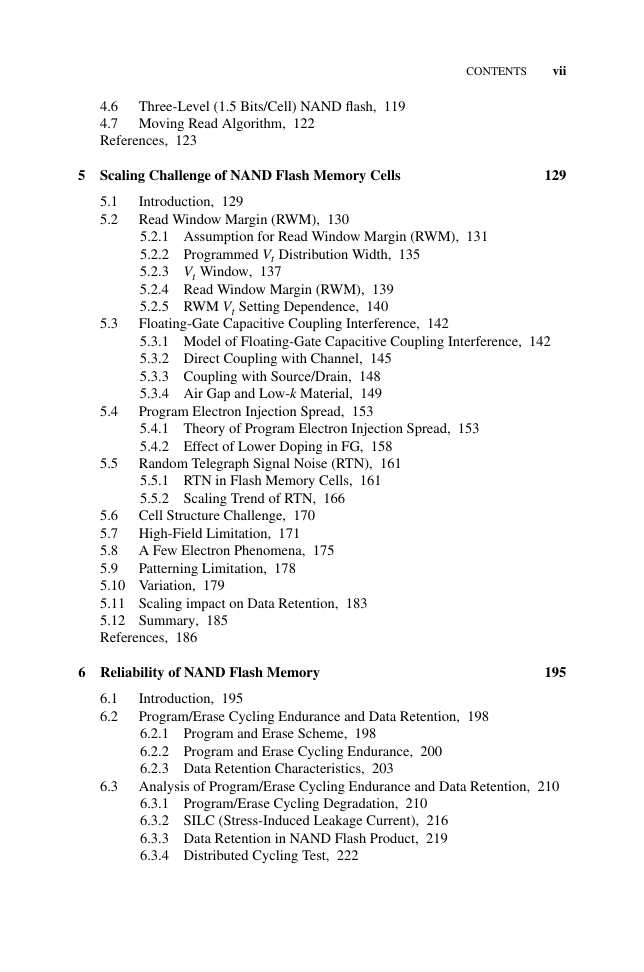
Three-Level (1.5 Bits/Cell) NAND flash, 119
4.6
4.7 Moving Read Algorithm, 122
References, 123
5 Scaling Challenge of NAND Flash Memory Cells
129
5.1
5.2
5.3
5.4
5.5
Introduction, 129
Read Window Margin (RWM), 130
5.2.1 Assumption for Read Window Margin (RWM), 131
5.2.2 Programmed Vt Distribution Width, 135
5.2.3 Vt Window, 137
5.2.4 Read Window Margin (RWM), 139
5.2.5 RWM Vt Setting Dependence, 140
Floating-Gate Capacitive Coupling Interference, 142
5.3.1 Model of Floating-Gate Capacitive Coupling Interference, 142
5.3.2 Direct Coupling with Channel, 145
5.3.3 Coupling with Source/Drain, 148
5.3.4 Air Gap and Low-k Material, 149
Program Electron Injection Spread, 153
5.4.1 Theory of Program Electron Injection Spread, 153
5.4.2 Effect of Lower Doping in FG, 158
Random Telegraph Signal Noise (RTN), 161
5.5.1 RTN in Flash Memory Cells, 161
5.5.2 Scaling Trend of RTN, 166
Cell Structure Challenge, 170
Patterning Limitation, 178
5.6
5.7 High-Field Limitation, 171
5.8 A Few Electron Phenomena, 175
5.9
5.10 Variation, 179
5.11 Scaling impact on Data Retention, 183
5.12 Summary, 185
References, 186
6 Reliability of NAND Flash Memory
195
6.1
6.2
Introduction, 195
Program/Erase Cycling Endurance and Data Retention, 198
6.2.1 Program and Erase Scheme, 198
6.2.2 Program and Erase Cycling Endurance, 200
6.2.3 Data Retention Characteristics, 203
6.3 Analysis of Program/Erase Cycling Endurance and Data Retention, 210
6.3.1 Program/Erase Cycling Degradation, 210
6.3.2 SILC (Stress-Induced Leakage Current), 216
6.3.3 Data Retention in NAND Flash Product, 219
6.3.4 Distributed Cycling Test, 222
�
viii
CONTENTS
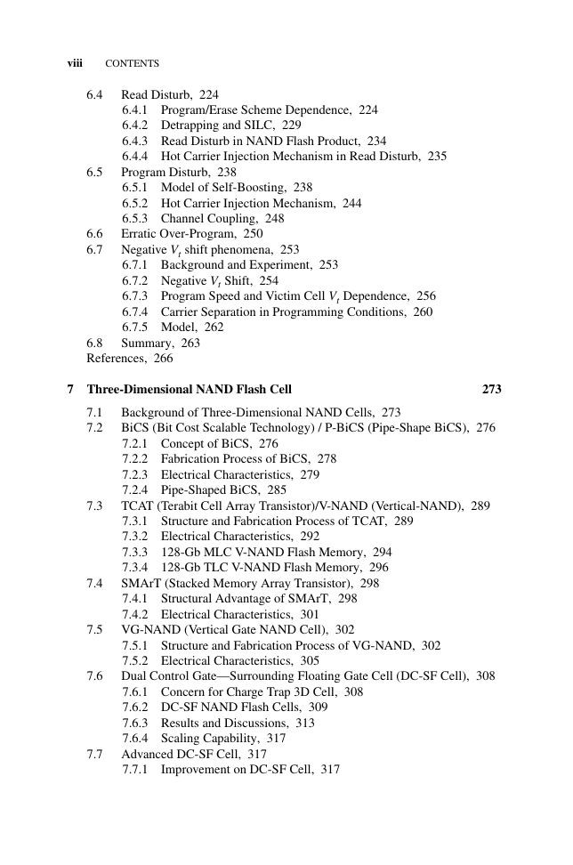
6.4
6.5
Read Disturb, 224
6.4.1 Program/Erase Scheme Dependence, 224
6.4.2 Detrapping and SILC, 229
6.4.3 Read Disturb in NAND Flash Product, 234
6.4.4 Hot Carrier Injection Mechanism in Read Disturb, 235
Program Disturb, 238
6.5.1 Model of Self-Boosting, 238
6.5.2 Hot Carrier Injection Mechanism, 244
6.5.3 Channel Coupling, 248
Erratic Over-Program, 250
6.6
6.7 Negative Vt shift phenomena, 253
6.7.1 Background and Experiment, 253
6.7.2 Negative Vt Shift, 254
6.7.3 Program Speed and Victim Cell Vt Dependence, 256
6.7.4 Carrier Separation in Programming Conditions, 260
6.7.5 Model, 262
Summary, 263
6.8
References, 266
7 Three-Dimensional NAND Flash Cell
273
7.1
7.2
7.3
7.4
Background of Three-Dimensional NAND Cells, 273
BiCS (Bit Cost Scalable Technology) / P-BiCS (Pipe-Shape BiCS), 276
7.2.1 Concept of BiCS, 276
7.2.2 Fabrication Process of BiCS, 278
7.2.3 Electrical Characteristics, 279
7.2.4 Pipe-Shaped BiCS, 285
TCAT (Terabit Cell Array Transistor)/V-NAND (Vertical-NAND), 289
7.3.1 Structure and Fabrication Process of TCAT, 289
7.3.2 Electrical Characteristics, 292
7.3.3
7.3.4
SMArT (Stacked Memory Array Transistor), 298
7.4.1 Structural Advantage of SMArT, 298
7.4.2 Electrical Characteristics, 301
128-Gb MLC V-NAND Flash Memory, 294
128-Gb TLC V-NAND Flash Memory, 296
7.5 VG-NAND (Vertical Gate NAND Cell), 302
7.5.1 Structure and Fabrication Process of VG-NAND, 302
7.5.2 Electrical Characteristics, 305
7.6 Dual Control Gate—Surrounding Floating Gate Cell (DC-SF Cell), 308
7.6.1 Concern for Charge Trap 3D Cell, 308
7.6.2 DC-SF NAND Flash Cells, 309
7.6.3 Results and Discussions, 313
7.6.4 Scaling Capability, 317
7.7 Advanced DC-SF Cell, 317
7.7.1
Improvement on DC-SF Cell, 317
�



 2023年江西萍乡中考道德与法治真题及答案.doc
 2012年重庆南川中考生物真题及答案.doc
 2013年江西师范大学地理学综合及文艺理论基础考研真题.doc
 2020年四川甘孜小升初语文真题及答案I卷.doc
 2020年注册岩土工程师专业基础考试真题及答案.doc
 2023-2024学年福建省厦门市九年级上学期数学月考试题及答案.doc
 2021-2022学年辽宁省沈阳市大东区九年级上学期语文期末试题及答案.doc
 2022-2023学年北京东城区初三第一学期物理期末试卷及答案.doc
 2018上半年江西教师资格初中地理学科知识与教学能力真题及答案.doc
 2012年河北国家公务员申论考试真题及答案-省级.doc
 2020-2021学年江苏省扬州市江都区邵樊片九年级上学期数学第一次质量检测试题及答案.doc
 2022下半年黑龙江教师资格证中学综合素质真题及答案.doc