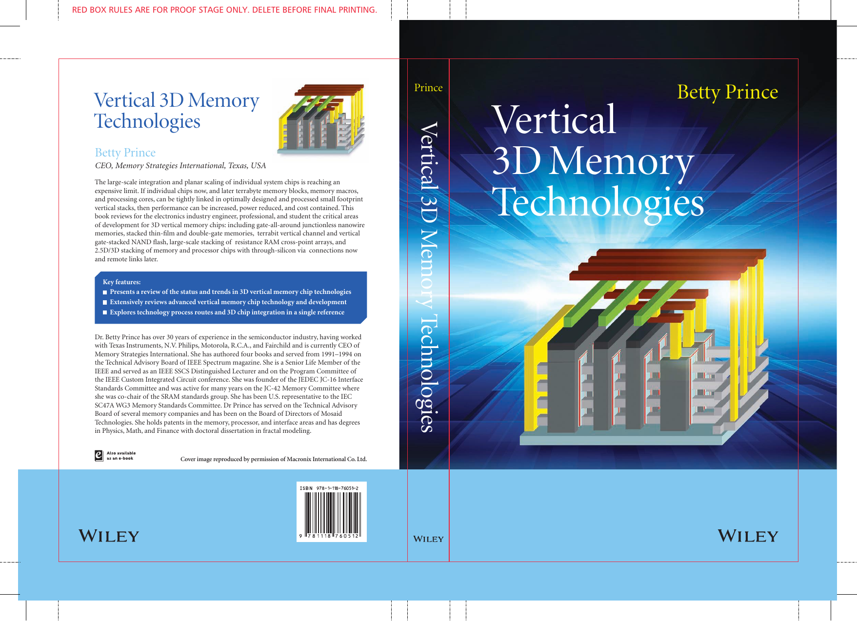
Cover
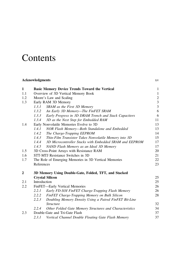
Contents
1 Basic Memory Device Trends Toward the Vertical
1.1 Overview of 3D Vertical Memory Book
1.2 Moore's Law and Scaling
1.3 Early RAM 3D Memory
1.3.1 SRAM as the First 3D Memory
1.3.2 An Early 3D Memory-The FinFET SRAM
1.3.3 Early Progress in 3D DRAM Trench and Stack Capacitors
1.3.4 3D as the Next Step for Embedded RAM
1.4 Early Nonvolatile Memories Evolve to 3D
1.4.1 NOR Flash Memory-Both Standalone and Embedded
1.4.2 The Charge-Trapping EEPROM
1.4.3 Thin-Film Transistor Takes Nonvolatile Memory into 3D
1.4.4 3D Microcontroller Stacks with Embedded SRAM and EEPROM
1.4.5 NAND Flash Memory as an Ideal 3D Memory
1.5 3D Cross-Point Arrays with Resistance RAM
1.6 STT-MTJ Resistance Switches in 3D
1.7 The Role of Emerging Memories in 3D Vertical Memories
References
2 3D Memory Using Double-Gate, Folded, TFT, and Stacked Crystal Silicon
2.1 Introduction
2.2 FinFET-Early Vertical Memories
2.2.1 Early FD-SOI FinFET Charge-Trapping Flash Memory
2.2.2 FinFET Charge-Trapping Memory on Bulk Silicon
2.2.3 Doubling Memory Density Using a Paired FinFET Bit-Line Structure
2.2.4 Other Folded Gate Memory Structures and Characteristics
2.3 Double-Gate and Tri-Gate Flash
2.3.1 Vertical Channel Double Floating Gate Flash Memory
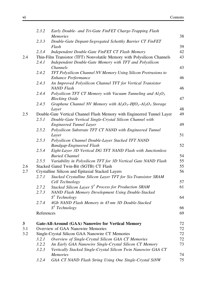
2.3.2 Early Double- and Tri-Gate FinFET Charge-Trapping Flash Memories
2.3.3 Double-Gate Dopant-Segregated Schottky Barrier CT FinFET Flash
2.3.4 Independent Double-Gate FinFET CT Flash Memory
2.4 Thin-Film Transistor (TFT) Nonvolatile Memory with Polysilicon Channels
2.4.1 Independent Double-Gate Memory with TFT and Polysilicon Channels
2.4.2 TFT Polysilicon Channel NV Memory Using Silicon Protrusions to Enhance Performance
2.4.3 An Improved Polysilicon Channel TFT for Vertical Transistor NAND Flash
2.4.4 Polysilicon TFT CT Memory with Vacuum Tunneling and Al2O3 Blocking Oxide
2.4.5 Graphene Channel NV Memory with Al2O3-HfOx-Al2O3 Storage Layer
2.5 Double-Gate Vertical Channel Flash Memory with Engineered Tunnel Layer
2.5.1 Double-Gate Vertical Single-Crystal Silicon Channel with Engineered Tunnel Layer
2.5.2 Polysilicon Substrate TFT CT NAND with Engineered Tunnel Layer
2.5.3 Polysilicon Channel Double-Layer Stacked TFT NAND Bandgap-Engineered Flash
2.5.4 Eight-Layer 3D Vertical DG TFT NAND Flash with Junctionless Buried Channel
2.5.5 Variability in Polysilicon TFT for 3D Vertical Gate NAND Flash
2.6 Stacked Gated Twin-Bit (SGTB) CT Flash
2.7 Crystalline Silicon and Epitaxial Stacked Layers
2.7.1 Stacked Crystalline Silicon Layer TFT for Six-Transistor SRAM Cell Technology
2.7.2 Stacked Silicon Layer S3 Process for Production SRAM
2.7.3 NAND Flash Memory Development Using Double-Stacked S3 Technology
2.7.4 4Gb NAND Flash Memory in 45 nm 3D Double-Stacked S3 Technology
References
3 Gate-All-Around (GAA) Nanowire for Vertical Memory
3.1 Overview of GAA Nanowire Memories
3.2 Single-Crystal Silicon GAA Nanowire CT Memories
3.2.1 Overview of Single-Crystal Silicon GAA CT Memories
3.2.2 An Early GAA Nanowire Single-Crystal Silicon CT Memory
3.2.3 Vertically Stacked Single-Crystal Silicon Twin Nanowire GAA CT Memories
3.2.4 GAA CT NAND Flash String Using One Single-Crystal SiNW
3.2.5 Single-Crystal SiNW CT Memory with High-κ Dielectric and Metal Gate
3.2.6 Improvement in Transient Vth Shift After Erase in 3D GAA NW SONOS
3.2.7 Semianalytical Model of GAA CT Memories
3.2.8 Nonvolatile GAA Single-Crystal Silicon Nanowire Memory on Bulk Substrate
3.3 Polysilicon GAA Nanowire CT Memories
3.3.1 Polysilicon CT Memories with NW Diameter Comparable to Polysilicon Grain Size
3.3.2 Various GAA Polysilicon NW Memory Configurations
3.3.3 Trapping Layer Enhanced Polysilicon NW SONOS
3.4 Junctionless GAA CT Nanowire Memories
3.4.1 3D Junctionless Vertical GAA Silicon NW SONOS Memories
3.4.2 Junctionless GAA SONOS Silicon Nanowire on Bulk Substrate for 3D NAND Stack
3.4.3 Modeling Erase in Cylindrical Junctionless CT Arrays
3.4.4 HfO2-Si3N4 Trap Layer in Junctionless Polycrystal GAA Memory Storage
3.5 3D Stacked Horizontal Nanowire Single-Crystal Silicon Memory
3.5.1 Process for 3D Stacked Horizontal NW Single-Crystal Silicon Memory
3.5.2 A Stacked Horizontal NW Single-Crystal Silicon NAND Flash Memory Development
3.6 Vertical Single-Crystal GAA CT Nanowire Flash Technology
3.6.1 Overview of Vertical Flash Using GAA SONOS Nanowire Technology
3.6.2 Vertical Single-Crystal Silicon 3D Flash Using GAA SONOS Nanowire
3.6.3 Fabrication of Two Independent GAA FETs on a Vertical SiNW
3.6.4 Vertical 3D Silicon Nanowire CT NAND Array
3.7 Vertical Channel Polysilicon GAA CT Memory
3.7.1 Multiple Vertical GAA Flash Cells Stacked Using Polysilicon NW Channel
3.7.2 Vth Shift Characteristics of Vertical GAA SONOS and/or TANOS Nonvolatile Memory
3.7.3 GAA Vertical Pipe CT Gate Replacement Technology
3.7.4 Bilayer Poly Channel Vertical Flash for 3D SONOS NAND
3.7.5 3D Vertical Pipe CT Low-Resistance (CoSi) Word-Line NAND Flash
3.7.6 Vertical Channel CT 3D NAND Flash Cell
3.7.7 Read Sensing for Thin-Body Vertical NAND
3.8 Graphene Channel Nonvolatile Memory with Al2O3-HfOx-Al2O3 Storage Layer
3.9 Cost Analysis for 3D GAA NAND Flash Considering Channel Slope
References
4 Vertical NAND Flash
4.1 Overview of 3D Vertical NAND Trends
4.1.1 3D Nonvolatile Memory Overview
4.1.2 Architectures of Various 3D NAND Flash Arrays
4.1.3 Scaling Trends for 2D and 3D NAND Cells
4.2 Vertical Channel (Pipe) CT NAND Flash Technology
4.2.1 BiCS CT Pipe NAND Flash Technology
4.2.2 Pipe-Shaped BiCS (P-BiCS) NAND Flash Technology
4.2.3 Vertical CT Vertical Recess Array Transistor (VRAT) Technology
4.2.4 Z-VRAT CT Memory Technology
4.2.5 Vertical NAND Chains-VSAT with ``PIPE´´ Process
4.2.6 Vertical CT PIPE NAND Flash with Damascene Metal Gate TCAT/VNAND
4.2.7 3D NAND Flash SB-CAT Stack
4.3 3D FG NAND Flash Cell Arrays
4.3.1 3D FG NAND with Extended Sidewall Control Gate
4.3.2 3D FG NAND with Separated-Sidewall Control Gate
4.3.3 3D FG NAND Flash Cell with Dual CGs and Surrounding FG (DC-SF)
4.3.4 3D Vertical FG NAND with Sidewall Control Pillar
4.3.5 Trap Characterization in 3D Vertical Channel NAND Flash
4.3.6 Program Disturb Characteristics of 3D Vertical NAND Flash
4.4 3D Stacked NAND Flash with Lateral BL Layers and Vertical Gate
4.4.1 Introduction to Horizontal BL and Vertical Gate NAND Flash
4.4.2 A 3D Vertical Gate NAND Flash Process and Device Considerations
4.4.3 Vertical Gate NAND Flash Integration with Eight Active Layers
4.4.4 3D Stacked CT TFT Bandgap-Engineered SONOS NAND Flash Memory
4.4.5 Horizontal Channel Vertical Gate 3D NAND Flash with PN Diode Decoding
4.4.6 3D Vertical Gate BE-SONOS NAND Program Inhibit with Multiple Island Gate Decoding
4.4.7 3D Vertical Gate NAND Flash BL Decoding and Page Operation
4.4.8 An Eight-Layer Vertical Gate 3D NAND Architecture with Split-Page BL
4.4.9 Various Innovations for 3D Stackable Vertical Gate
4.4.10 Variability Considerations in 2D Vertical Gate 3D NAND Flash
4.4.11 An Etching Technology for Vertical Multilayers for 3D Vertical Gate NAND Flash
4.4.12 Interference, Disturb, and Programming Algorithms for MLC Vertical Gate NAND
4.4.13 3D Vertical Gate NAND Flash Program and Read and Fail-Bit Detection
4.4.14 3D p-Channel Stackable NAND Flash with Band-to-Band Tunnel Programming
4.4.15 A Bit-Alterable 3D NAND Flash with n-Channel and p-Channel NAND
References
5 3D Cross-Point Array Memory
5.1 Overview of Cross-Point Array Memory
5.2 A Brief Background of Cross-Point Array Memories
5.2.1 Construction of a Basic Cross-Point Array
5.2.2 Stacking Multibit Cross-Point Arrays
5.2.3 Methods of Stacking Cross-Point Arrays
5.2.4 Stacking Cross-Point Layers for High Density
5.2.5 An Example of Unipolar ReRAM
5.2.6 An Example of a Bipolar ReRAM
5.2.7 Basic Cross-Point Array Operation with a Diode Selector
5.2.8 Early Test Chip Using a ReRAM Cross-Point Array with Diode Selector
5.3 Low-Resistance Interconnects for Cross-Point Arrays
5.3.1 Model of Low Resistance Interconnects for Cross-Point Arrays
5.3.2 A Cross-Point Array Grid with Low-Resistivity Nanowires
5.3.3 A Cross-Point Array Using Two Nickel Core Nanowires
5.3.4 Resistive Memory Using Single-Wall Carbon Nanotubes
5.4 Cross-Point Array Memories Without Cell Selectors
5.4.1 Early Model of Bipolar Resistive Switch in Selectorless Cross-Point Array
5.4.2 Sneak Path Leakage in a Selectorless Cross-Point Array
5.4.3 Effect of Parasitic Resistance on Maximum Size of a Selectorless Cross-Point Array
5.4.4 Effect of Nonlinearity on I-V Characteristics of Selectorless Memory Element
5.4.5 Self-Rectifying ReRAM Requirements in Cross-Point Arrays
5.4.6 A Cross-Point Array Model for Line Resistance and Nonlinear Devices
5.5 Examples of Selectorless Cross-Point Arrays
5.5.1 Example of Nonlinearity in a Selectorless Cross-Point Array
5.5.2 Example of High-Resistive Memory Element in Selectorless Cross-Point Array
5.5.3 Design Techniques for Nonlinear Selectorless Cross-Point Arrays Using ReRAMs
5.5.4 Film Thickness and Scaling Effects in Cross-Point Selectorless ReRAM
5.5.5 Vertical HfOx ReRAM 3D Cross-Point Array Without Cell Selector
5.5.6 Dopant Selection Rules for Tuning HfOx ReRAM Characteristics
5.5.7 High-Resistance CB-ReRAM Memory Element to Avoid Sneak Current
5.5.8 Electromechanical Diode Cell for a Cross-Point Nonvolatile Memory Array
5.6 Unipolar Resistance RAMs with Diode Selectors in Cross-Point Arrays
5.6.1 Overview of Unipolar ReRAMS with Diode Selectors in Cross-Point Arrays
5.6.2 A Unipolar ReRAM with Silicon Diode for Cross-Point Array
5.6.3 CuOx-InZnOx Heterojunction Thin-Film Diode with NiO ReRAM
5.6.4 Unipolar NiO ReRAM Ireset and SET-RESET Instability
5.6.5 HfOx-AlOy Unipolar ReRAM with Silicon Diode Selector in Cross-Point Array
5.6.6 TiN-TaOx-Pt MIM Selector for Pt-TaOx-Pt Unipolar ReRAM Cross-Point Array
5.6.7 Self-Rectifying Unipolar Ni-HfOx Schottky Barrier ReRAM
5.6.8 Schottky Barriers for Self-Rectifying Unidirectional Cross-Point Array
5.6.9 Thermally Induced Set Operation for Unipolar ReRAM with Diode Selector
5.7 Unipolar PCM with Two-Terminal Diodes for Cross-Point Array
5.7.1 Background of Phase-Change Memory in a Cross-Point Array
5.7.2 PCMs in Cross-Point Arrays with Polysilicon Diodes
5.7.3 Cross-Point Array with PCM and Carbon Nanotube Electrode
5.7.4 Cross-Point Array with MIEC Access Devices and PCM Elements
5.7.5 Threshold Switching Access Devices for ReRAM Cross-Point Arrays
5.7.6 p-n Diode Selection Devices for PCM
5.7.7 Epitaxial Diode Selector for PCM in Cross-Point Arrays
5.7.8 Dual-Trench Epitaxial Diode Array for High-Density PCM
5.8 Bipolar Resistance RAMS With Selector Devices in Cross-Point Arrays
5.8.1 VO2 Select Device for Bipolar ReRAM in Cross-Point Array
5.8.2 Threshold Select Devices for Bipolar Memory Elements in Cross-Point Arrays
5.8.3 Vertical Bipolar Switching Polysilicon n-p-n Diode for Cross-Point Array
5.8.4 Two-Terminal Diode Steering Element for 3D Cross-Point ReRAM Array
5.8.5 Varistor-Type Bidirectional Switch for 3D Bipolar ReRAM Array
5.8.6 Bidirectional Threshold Vacuum Switch for 3D 4F2 Cross-Point Array
5.8.7 Bidirectional Schottky Diode Selector
5.8.8 Bipolar ReRAM with Schottky Self-Rectifying Behavior in the LRS
5.8.9 Self-Rectifying Bipolar ReRAM Using Schottky Barrier at Ta-TaOx Interface
5.8.10 Diode Effect of Pt-In2Ga2ZnO7 Layer in TiO2-type ReRAM
5.8.11 Confined NbO2 as a Selector in Bipolar ReRAMs
5.9 Complementary Switching Devices and Arrays
5.9.1 Complementary Resistive Switching for Dense Crossbar Arrays
5.9.2 CRS Memory Using Amorphous Carbon and CNTs
5.9.3 Complementary Switching in Metal-Oxide ReRAM for Crossbar Arrays
5.9.4 CRSs Using a Heterodevice
5.9.5 Self-Selective W-VO2-Pt ReRAM to Reduce Sneak Current in ReRAM Arrays
5.9.6 Hybrid Nb2O5-NbO2 ReRAM with Combined Memory and Selector
5.9.7 Analysis of Complementary ReRAM Switching
5.9.8 Complementary Stacked Bipolar ReRAM Cross-Point Arrays
5.9.9 Complementary Switching Oxide-Based Bipolar ReRAM
5.10 Toward Manufacturable ReRAM Cells and Cross-point Arrays
5.10.1 28 nm ReRAM and Diode Cross-Point Array in CMOS-Compatible Process
5.10.2 Double-Layer 3D Vertical ReRAM for High-Density Arrays
5.10.3 Study of Cell Performance for Different Stacked ReRAM Geometries
5.11 STT Magnetic Tunnel Junction Resistance Switches in Cross-Point Array Architecture
5.11.1 High-Density Cross-Point STT Magnetic Tunnel Junction Architecture
References
6 3D Stacking of RAM-Processor Chips Using TSV
6.1 Overview of 3D Stacking of RAM-Processor Chips with TSV
6.2 Architecture and Design of TSV RAM-Processor Chips
6.2.1 Overview of Architecture and Design of Vertical TSV Connected Chips
6.2.2 Repartitioning for Performance by Increasing the Number of Memory Banks
6.2.3 Using a Global Clock Distribution Technique to Improve Performance
6.2.4 Stacking eDRAM Cache and Processor for Improved Performance
6.2.5 Using Decoupling Scheduling of the Memory Controller to Improve Performance
6.2.6 Repartitioning Multicore Processors and Stacked RAM for Improved Performance
6.2.7 Increasing Performance and Lowering Power in Low-Power Mobile Systems
6.2.8 Increasing Performance of Memory Hierarchies with 3D TSV Integration
6.2.9 Adding Storage-Class Memory to the Memory Hierarchy
6.2.10 Improving Performance Using 3D Stacked RAM Modeling
6.3 Process and Fabrication of Vertical TSV for Memory and Logic
6.3.1 Passive TSV Interposers for Stacked Memory-Logic Integration
6.3.2 Process Fabrication Methods and Foundries for Early 2.5D and 3D Integration
6.3.3 Integration with TSV Using a High-κ-Metal Gate CMOS Process
6.3.4 Processor with Deep Trench DRAM TSV Stacks and High-κ-Metal Gate
6.4 Process and Fabrication Issues of TSV 3D Stacking Technology
6.4.1 Using Copper TSV for 3D Stacking
6.4.2 Air Gaps for High-Performance TSV Interconnects for 3D ICs
6.5 Fabrication of TSVs
6.5.1 Using TSVs at Various Stages in the Process
6.5.2 Stacked Chips using Via-Middle Technology
6.6 Energy Efficiency Considerations of 3D Stacked Memory-Logic Chip Systems
6.6.1 Overview of Energy Efficiency in 3D Stacked Memory-Logic Chip Systems
6.6.2 Energy Efficiency for a 3D TSV Integrated DRAM-Controller System
6.6.3 Adding an SRAM Row Cache to Stacked 3D DRAM to Minimize Energy
6.6.4 Power Delivery Networks in 3D ICs
6.6.5 Using Near-Threshold Computing for Power Reduction in a 3D TSV System
6.7 Thermal Characterization Analysis and Modeling of RAM-Logic Stacks
6.7.1 Thermal Management of Hot Spots in 3D Chips
6.7.2 Thermal Management in 3D Chips Using an Interposer with Embedded TSV
6.7.3 Thermal Management of TSV DRAM Stacks with Logic
6.7.4 Thermal Management of a 3D TSV SRAM on Logic Stack
6.8 Testing of 3D Stacked TSV System Chips
6.8.1 Using BIST to Reduce Testing for a Logic and DRAM System Stack
6.8.2 Efficient BISR and Redundancy Allocation in 3D RAM-Logic Stacks
6.8.3 Direct Testing of Early SDRAM Stacks
6.9 Reliability Considerations with 3D TSV RAM-Processor Chips
6.9.1 Overview of Reliability Issues in 3D TSV Stacked RAM-Processor Chips
6.9.2 Variation Issues in Stacked 3D TSV RAM-Processor Chips
6.9.3 Switching and Decoupling Noise in a 3D TSV-Based System
6.9.4 TSV-Induced Mechanical Stress in CMOS
6.10 Reconfiguring Stacked TSV Memory Architectures for Improved Performance
6.10.1 Overview of Potential for Reconfigured Stacked Architectures
6.10.2 3D TSV-based 3D SRAM for High-Performance Platforms
6.10.3 Waveform Capture with 100 GB/s I/O, 4096 TSVs and an Active Si Interposer
6.10.4 3D Stacked FPGA and ReRAM Configuration Memory
6.10.5 Cache Architecture to Configure Stacked DRAM to Specific Applications
6.10.6 Network Platform for Stacked Memory-Processor Architectures
6.10.7 Multiplexing Signals to Reduce Number of TSVs in IC Die Stacking
6.10.8 3D Hybrid Cache with MRAM and SRAM Stacked on Processor Cores
6.10.9 CMOS FPGA and Routing Switches Made with ReRAM Devices
6.10.10 Dynamic Configurable SRAM Stacked with Various Logic Chips
6.11 Stacking Memories Using Noncontact Connections with Inductive Coupling
6.11.1 Overview of Noncontact Inductive Coupling of Stacked Memory
6.11.2 Early Concepts of Inductive-Coupling Connections of Stacked Memory Chips
6.11.3 Evolution of Inductive-Coupling Connections of NAND Flash Stacks
6.11.4 TCI for Replacing Stacking with TSV Connections
6.11.5 Processor-SRAM 3D Integration Using Inductive Coupling
6.11.6 Optical Interface for Future 3D Stacked Chip Connections
References
Index
End User License Agreement





 2023年江西萍乡中考道德与法治真题及答案.doc
 2012年重庆南川中考生物真题及答案.doc
 2013年江西师范大学地理学综合及文艺理论基础考研真题.doc
 2020年四川甘孜小升初语文真题及答案I卷.doc
 2020年注册岩土工程师专业基础考试真题及答案.doc
 2023-2024学年福建省厦门市九年级上学期数学月考试题及答案.doc
 2021-2022学年辽宁省沈阳市大东区九年级上学期语文期末试题及答案.doc
 2022-2023学年北京东城区初三第一学期物理期末试卷及答案.doc
 2018上半年江西教师资格初中地理学科知识与教学能力真题及答案.doc
 2012年河北国家公务员申论考试真题及答案-省级.doc
 2020-2021学年江苏省扬州市江都区邵樊片九年级上学期数学第一次质量检测试题及答案.doc
 2022下半年黑龙江教师资格证中学综合素质真题及答案.doc