Keysight EEsof EDA
Getting Started with Advanced Design System
(ADS)
Demo Guide
�
02 | Keysight | Getting Started with Advanced Design System (ADS) - Demo Guide
Getting Started with ADS
This tutorial will introduce the basic structure of ADS workspaces, libraries and cells. This
includes design capture, simulation, and displaying simulation results.
Note: Workspaces in ADS 2011 and later replace projects from earlier ADS versions.
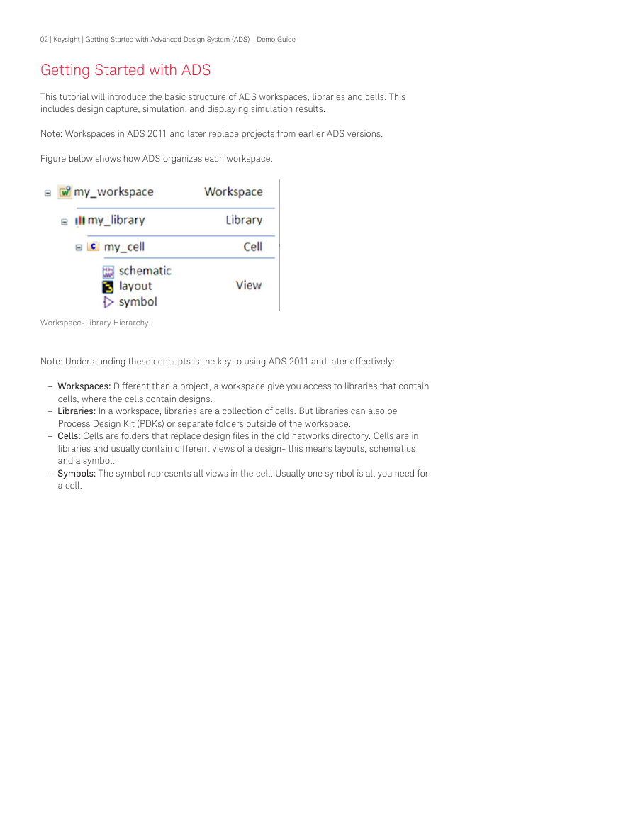
Figure below shows how ADS organizes each workspace.
Workspace-Library Hierarchy.
Note: Understanding these concepts is the key to using ADS 2011 and later effectively:
– Workspaces: Different than a project, a workspace give you access to libraries that contain
cells, where the cells contain designs.
– Libraries: In a workspace, libraries are a collection of cells. But libraries can also be
Process Design Kit (PDKs) or separate folders outside of the workspace.
– Cells: Cells are folders that replace design files in the old networks directory. Cells are in
libraries and usually contain different views of a design- this means layouts, schematics
and a symbol.
– Symbols: The symbol represents all views in the cell. Usually one symbol is all you need for
a cell.
�
03 | Keysight | Getting Started with Advanced Design System (ADS) - Demo Guide
Step 1 - Create a New Workspace
1. Launch ADS and from the ADS main window select File > New > Workspace. Or click on
.
this icon
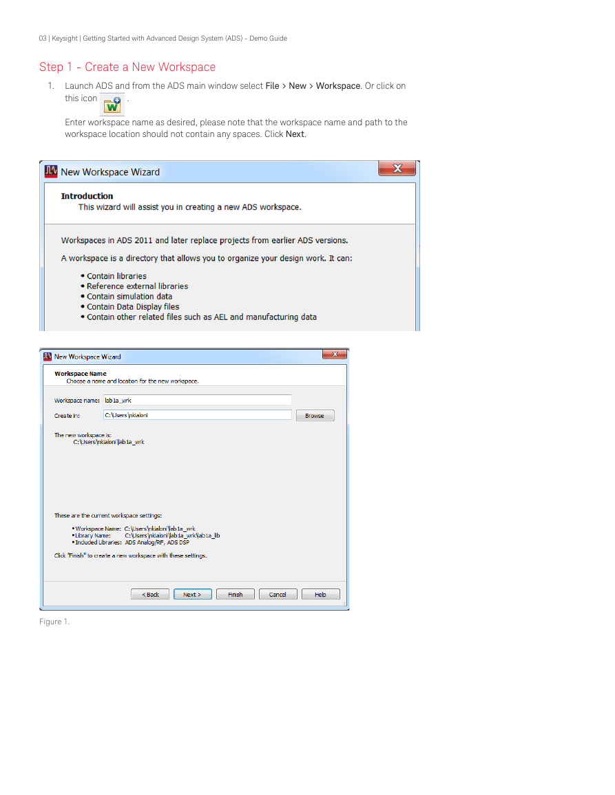
Enter workspace name as desired, please note that the workspace name and path to the
workspace location should not contain any spaces. Click Next.
Figure 1.
�
04 | Keysight | Getting Started with Advanced Design System (ADS) - Demo Guide
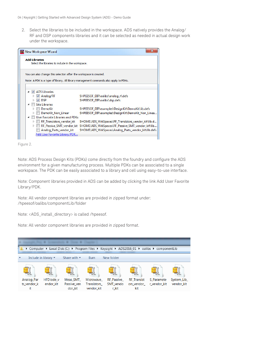
2. Select the libraries to be included in the workspace. ADS natively provides the Analog/
RF and DSP components libraries and it can be selected as needed in actual design work
under the workspace.
Figure 2.
Note: ADS Process Design Kits (PDKs) come directly from the foundry and configure the ADS
environment for a given manufacturing process. Multiple PDKs can be associated to a single
workspace. The PDK can be easily associated to a library and cell using easy-to-use interface.
Note: Component libraries provided in ADS can be added by clicking the link Add User Favorite
Library/PDK.
Note: All vendor component libraries are provided in zipped format under:
/hpeesof/oalibs/componentLib/folder
Note:
is called /hpeesof.
Note: All vendor component libraries are provided in zipped format.
�05 | Keysight | Getting Started with Advanced Design System (ADS) - Demo Guide
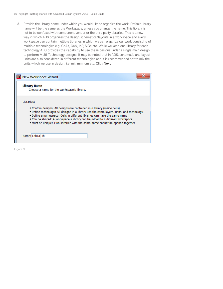
3. Provide the library name under which you would like to organize the work. Default library
name will be the same as the Workspace, unless you change the name. This library is
not to be confused with component vendor or the third party libraries. This is a new
way in which ADS organizes the design schematics/layouts in a workspace and every
workspace can contain multiple libraries in which we can organize our work consisting of
multiple technologies e.g. GaAs, GaN, InP, SiGe etc. While we keep one library for each
technology ADS provides the capability to use these designs under a single main design
to perform Multi-Technology designs. It may be noted that in ADS, schematic and layout
units are also considered in different technologies and it is recommended not to mix the
units which we use in design. i.e. mil, mm, um etc. Click Next.
Figure 3.
�
06 | Keysight | Getting Started with Advanced Design System (ADS) - Demo Guide
4. Select the preferred units to be used during the design. In the present example, select
0.0001 mil layout resolution.
Figure 4.
5. Click Next and see the summary of the workspace and click Finish and a blank
workspace as shown below will appear. We are ready to create our schematic or layout
designs in the newly created workspace.
Figure 5.
�
07 | Keysight | Getting Started with Advanced Design System (ADS) - Demo Guide
Step 2 - Creating Schematic Design
Usually circuit design will start from schematic entry. To start the schematic design we can
begin from File > New > Schematic or by clicking on the Schematic icon
window toolbar.
on the main
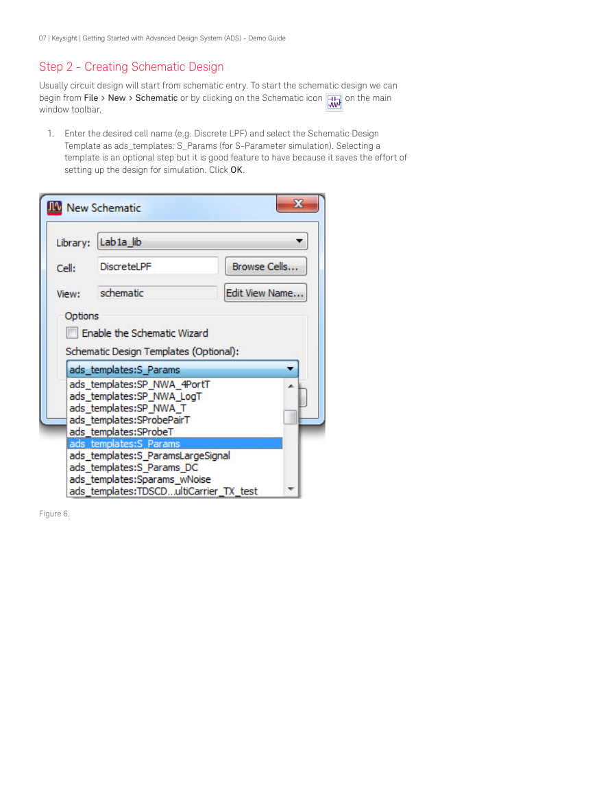
1. Enter the desired cell name (e.g. Discrete LPF) and select the Schematic Design
Template as ads_templates: S_Params (for S-Parameter simulation). Selecting a
template is an optional step but it is good feature to have because it saves the effort of
setting up the design for simulation. Click OK.
Figure 6.
�
08 | Keysight | Getting Started with Advanced Design System (ADS) - Demo Guide
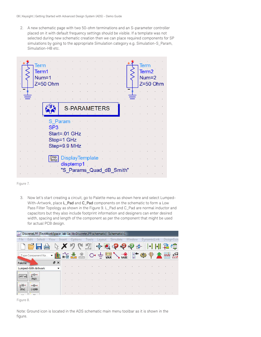
2. A new schematic page with two 50-ohm terminations and an S-parameter controller
placed on it with default frequency settings should be visible. If a template was not
selected during new schematic creation then we can place required components for SP
simulations by going to the appropriate Simulation category e.g. Simulation-S_Param,
Simulation-HB etc.
Figure 7.
3. Now let’s start creating a circuit, go to Palette menu as shown here and select Lumped-
With-Artwork, place L_Pad and C_Pad components on the schematic to form a Low
Pass Filter Topology as shown in the Figure 9. L_Pad and C_Pad are normal inductor and
capacitors but they also include footprint information and designers can enter desired
width, spacing and length of the component as per the component that might be used
for actual PCB design.
Figure 8.
Note: Ground icon is located in the ADS schematic main menu toolbar as it is shown in the
figure.
�



 2023年江西萍乡中考道德与法治真题及答案.doc
 2012年重庆南川中考生物真题及答案.doc
 2013年江西师范大学地理学综合及文艺理论基础考研真题.doc
 2020年四川甘孜小升初语文真题及答案I卷.doc
 2020年注册岩土工程师专业基础考试真题及答案.doc
 2023-2024学年福建省厦门市九年级上学期数学月考试题及答案.doc
 2021-2022学年辽宁省沈阳市大东区九年级上学期语文期末试题及答案.doc
 2022-2023学年北京东城区初三第一学期物理期末试卷及答案.doc
 2018上半年江西教师资格初中地理学科知识与教学能力真题及答案.doc
 2012年河北国家公务员申论考试真题及答案-省级.doc
 2020-2021学年江苏省扬州市江都区邵樊片九年级上学期数学第一次质量检测试题及答案.doc
 2022下半年黑龙江教师资格证中学综合素质真题及答案.doc