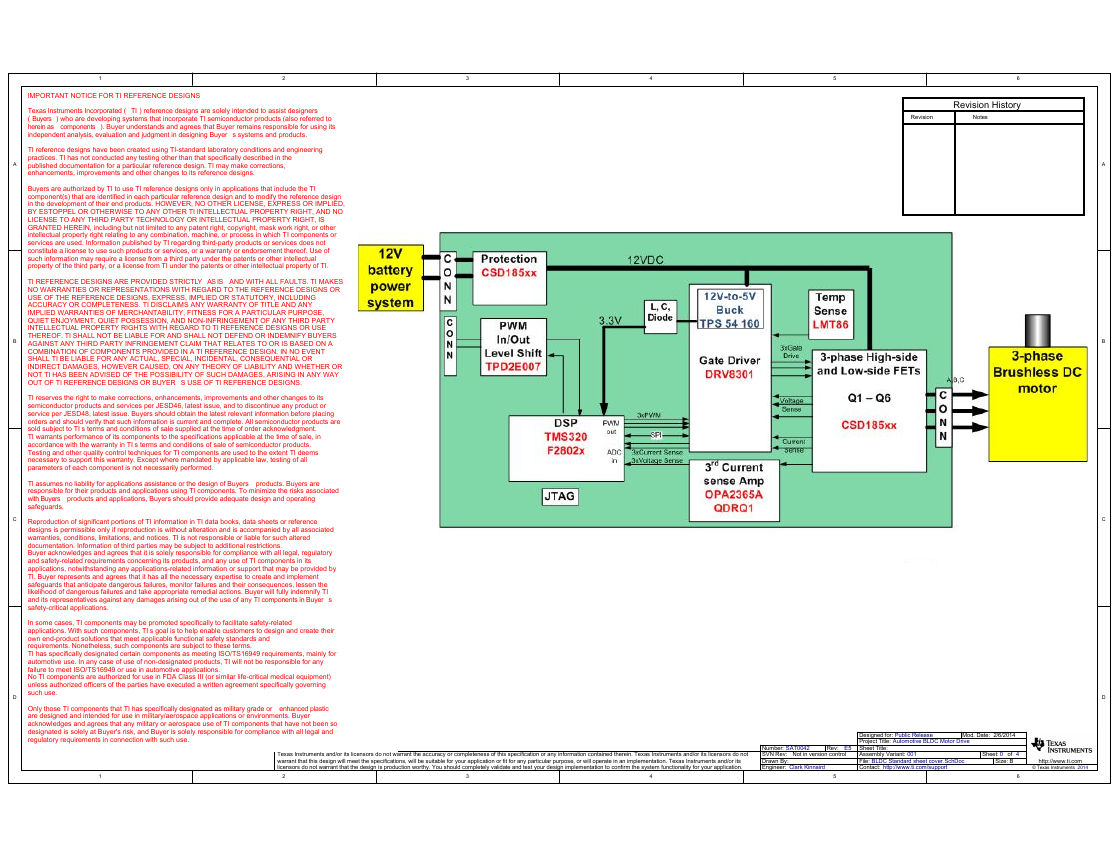
112233445566DDCCBBAA042/6/2014BLDC Standard sheet cover.SchDocSheet Title:Size:Mod. Date:File:Sheet:ofBhttp://www.ti.comContact:http://www.ti.com/supportAutomotive BLDC Motor DriveProject Title:Designed for:Public ReleaseAssembly Variant:001© Texas Instruments2014Drawn By:Engineer:Clark KinnairdTexas Instruments and/or its licensors do not warrant the accuracy or completeness of this specification or any information contained therein. Texas Instruments and/or its licensors do not warrant that this design will meet the specifications, will be suitable for your application or fit for any particular purpose, or will operate in an implementation. Texas Instruments and/or its licensors do not warrant that the design is production worthy. You should completely validate and test your design implementation to confirm the system functionality for your application.Not in version controlSVN Rev:SAT0042Number:Rev:E5Revision HistoryRevisionNotesIMPORTANT NOTICE FOR TI REFERENCE DESIGNSTexas Instruments Incorporated (?TI?) reference designs are solely intended to assist designers(?Buyers?) who are developing systems that incorporate TI semiconductor products (also referred toherein as ?components?). Buyer understands and agrees that Buyer remains responsible for using itsindependent analysis, evaluation and judgment in designing Buyer?s systems and products.TI reference designs have been created using TI-standard laboratory conditions and engineeringpractices. TI has not conducted any testing other than that specifically described in thepublished documentation for a particular reference design. TI may make corrections,enhancements, improvements and other changes to its reference designs.Buyers are authorized by TI to use TI reference designs only in applications that include the TIcomponent(s) that are identified in each particular reference design and to modify the reference designin the development of their end products. HOWEVER, NO OTHER LICENSE, EXPRESS OR IMPLIED,BY ESTOPPEL OR OTHERWISE TO ANY OTHER TI INTELLECTUAL PROPERTY RIGHT, AND NOLICENSE TO ANY THIRD PARTY TECHNOLOGY OR INTELLECTUAL PROPERTY RIGHT, ISGRANTED HEREIN, including but not limited to any patent right, copyright, mask work right, or otherintellectual property right relating to any combination, machine, or process in which TI components orservices are used. Information published by TI regarding third-party products or services does notconstitute a license to use such products or services, or a warranty or endorsement thereof. Use ofsuch information may require a license from a third party under the patents or other intellectualproperty of the third party, or a license from TI under the patents or other intellectual property of TI.TI REFERENCE DESIGNS ARE PROVIDED STRICTLY ?AS IS? AND WITH ALL FAULTS. TI MAKESNO WARRANTIES OR REPRESENTATIONS WITH REGARD TO THE REFERENCE DESIGNS ORUSE OF THE REFERENCE DESIGNS, EXPRESS, IMPLIED OR STATUTORY, INCLUDINGACCURACY OR COMPLETENESS. TI DISCLAIMS ANY WARRANTY OF TITLE AND ANYIMPLIED WARRANTIES OF MERCHANTABILITY, FITNESS FOR A PARTICULAR PURPOSE,QUIET ENJOYMENT, QUIET POSSESSION, AND NON-INFRINGEMENT OF ANY THIRD PARTYINTELLECTUAL PROPERTY RIGHTS WITH REGARD TO TI REFERENCE DESIGNS OR USETHEREOF. TI SHALL NOT BE LIABLE FOR AND SHALL NOT DEFEND OR INDEMNIFY BUYERSAGAINST ANY THIRD PARTY INFRINGEMENT CLAIM THAT RELATES TO OR IS BASED ON ACOMBINATION OF COMPONENTS PROVIDED IN A TI REFERENCE DESIGN. IN NO EVENTSHALL TI BE LIABLE FOR ANY ACTUAL, SPECIAL, INCIDENTAL, CONSEQUENTIAL ORINDIRECT DAMAGES, HOWEVER CAUSED, ON ANY THEORY OF LIABILITY AND WHETHER ORNOT TI HAS BEEN ADVISED OF THE POSSIBILITY OF SUCH DAMAGES, ARISING IN ANY WAYOUT OF TI REFERENCE DESIGNS OR BUYER?S USE OF TI REFERENCE DESIGNS.TI reserves the right to make corrections, enhancements, improvements and other changes to itssemiconductor products and services per JESD46, latest issue, and to discontinue any product orservice per JESD48, latest issue. Buyers should obtain the latest relevant information before placingorders and should verify that such information is current and complete. All semiconductor products aresold subject to TI?s terms and conditions of sale supplied at the time of order acknowledgment.TI warrants performance of its components to the specifications applicable at the time of sale, inaccordance with the warranty in TI?s terms and conditions of sale of semiconductor products.Testing and other quality control techniques for TI components are used to the extent TI deemsnecessary to support this warranty. Except where mandated by applicable law, testing of allparameters of each component is not necessarily performed.TI assumes no liability for applications assistance or the design of Buyers? products. Buyers areresponsible for their products and applications using TI components. To minimize the risks associatedwith Buyers? products and applications, Buyers should provide adequate design and operatingsafeguards.Reproduction of significant portions of TI information in TI data books, data sheets or referencedesigns is permissible only if reproduction is without alteration and is accompanied by all associatedwarranties, conditions, limitations, and notices. TI is not responsible or liable for such altereddocumentation. Information of third parties may be subject to additional restrictions.Buyer acknowledges and agrees that it is solely responsible for compliance with all legal, regulatoryand safety-related requirements concerning its products, and any use of TI components in itsapplications, notwithstanding any applications-related information or support that may be provided byTI. Buyer represents and agrees that it has all the necessary expertise to create and implementsafeguards that anticipate dangerous failures, monitor failures and their consequences, lessen thelikelihood of dangerous failures and take appropriate remedial actions. Buyer will fully indemnify TIand its representatives against any damages arising out of the use of any TI components in Buyer?ssafety-critical applications.In some cases, TI components may be promoted specifically to facilitate safety-relatedapplications. With such components, TI?s goal is to help enable customers to design and create theirown end-product solutions that meet applicable functional safety standards andrequirements. Nonetheless, such components are subject to these terms.TI has specifically designated certain components as meeting ISO/TS16949 requirements, mainly forautomotive use. In any case of use of non-designated products, TI will not be responsible for anyfailure to meet ISO/TS16949 or use in automotive applications.No TI components are authorized for use in FDA Class III (or similar life-critical medical equipment)unless authorized officers of the parties have executed a written agreement specifically governingsuch use.Only those TI components that TI has specifically designated as military grade or ?enhanced plastic?are designed and intended for use in military/aerospace applications or environments. Buyeracknowledges and agrees that any military or aerospace use of TI components that have not been sodesignated is solely at Buyer's risk, and Buyer is solely responsible for compliance with all legal andregulatory requirements in connection with such use.�
COJ1
PIJ101
PIJ101
PIJ102
PIJ102
PIJ103
PIJ103
PIJ104
PIJ104
NLVBATT
COL1
PIL101
PIL101
PIL102
PIL102
COTP1
PITP101
PITP101
COF1
PIF101
PIF101
PIF102
PIF102
PIC501
PIC501
PIC502
PIC502
COC5
PIC201
PIC201
PIC202
PIC202
PIC601
PIC601
PIC602
PIC602
COC2
COC6
PIC401
PIC401
PIC402
PIC402
COC4
COC1
PIC101
PIC101
PIC102
PIC102
COC3
PIC301
PIC301
PIC302
PIC302
NLBATT0GND
PIQ105
PIQ106
PIQ107
PIQ108
PIQ109
PIQ105
PIQ106
PIQ107
PIQ108
PIQ109
PIQ101
PIQ102
PIQ103
PIQ101
PIQ102
PIQ103
COQ1
COR1
PIR102
PIR102
PIR101
PIR101
PIQ104
PIQ104
COTP2
COTP3
COTP4
PITP201
PITP201
PITP301
PITP301
PITP401
PITP401
COD1
PID101 PID102
PID102
PID101
PIR402
PIR402
COR4
PIR401
PIR401
COJ2
PIJ203
PIJ203
PIJ202
PIJ202
PIJ201
PIJ201
NLPWM0IN
COR5
COR6
PIR501
PIR501
PIR502
PIR502
PIR602
PIR602
PIR601
PIR601
NLPWM0OUT
COR8
PIR801
PIR801
PIR802
PIR802
COU1
PIU101
PIU101
PIU102
PIU102
PIC701
PIC701
PIC702
PIC702
COC7
PIR702
PIR702
COR7
PIR701
PIR701
PIU103
PIU103
PIR202
PIR202
COR2
PIR201
PIR201
COU8A
PIU801
PIU801
COR3
PIR301
PIR301
PIR302
PIR302
PIU802
PIU802
PIU803
PIU803
PIU808
PIU808
PIU804
PIU804
COR9
COR10
PIR902
PIR902
PIR901
PIR901
PIR1001
PIR1001
PIR1002
PIR1002
PIR1202
PIR1202
COR12
PIR1201
PIR1201
PIR1302
PIR1302
COR13
PIR1301
PIR1301
PIR1102
PIR1102
COR11
PIR1101
PIR1101
PIU807
PIU807
COU8B
PIU806
PIU806
PIU805
PIU805
PIU808
PIU808
PIU804
PIU804
COR14
PIR1401
PIR1401
PIR1402
PIR1402
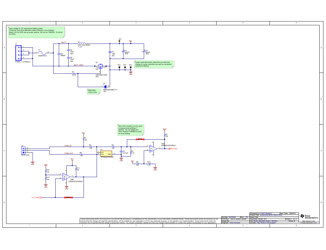
112233445566DDCCBBAA142/6/2014BLDC Standard sheet 1.SchDocSheet Title:Size:Mod. Date:File:Sheet:ofBhttp://www.ti.comContact:http://www.ti.com/supportAutomotive BLDC Motor DriveProject Title:Designed for:Public ReleaseAssembly Variant:001© Texas Instruments2014Drawn By:Engineer:Clark KinnairdTexas Instruments and/or its licensors do not warrant the accuracy or completeness of this specification or any information contained therein. Texas Instruments and/or its licensors do not warrant that this design will meet the specifications, will be suitable for your application or fit for any particular purpose, or will operate in an implementation. Texas Instruments and/or its licensors do not warrant that the design is production worthy. You should completely validate and test your design implementation to confirm the system functionality for your application.Not in version controlSVN Rev:SAT0042Number:Rev:E5GNDDC+680pFC54.7µHL1SRP1250-4R7M15V21D1MMSZ5245BS-7-F52.3kR147,81,2,35,6,40VQ1CSD18501Q5AOUT_PWMDC+IN_PWM3p3VGNDDC+PWM_INPWM_OUTIO11IO22GND3U1TPD2E007DCKR0.01µFC7TP2TP1TP4TP31234J1CONN_1-1318300-4VBATTBATT_GNDGND0R3DNP0R14DNPGNDGND3p3VDC+GND20kR92.7kR102.7kR710kR1210kR1310kR410kR210kR1110kR61.5kR81.5kR510µF50VC4220µF50VC3220µF50VC110µF50VC210µF50VC6567BV+V-84U8BLM2903VQPWRQ1231AV+V-84U8ALM2903VQPWRQ1123J222-27-203105200101Z21F1Input voltage is 12V automotive battery powerCustomer may have alternate supply protection circuit design.Need 3.3V for DSP and op amps, approx 140 mA for TMS320, 10 mA for op amps.ABS.MAX. VGS is 20VLarge value electrolytic capacitors provide bulk charge for motor transitions as well as conducted emissions filtering.Zero Ohm resistors can be used to bypass level-shifting if desired. Do not install zero Ohm resistor if LM2903 is used for level shifting.�
COL2
PIL201
PIL201
PIL202
PIL202
COL4
PIL401
PIL401
PIL402
PIL402
COL5
PIL501
PIL501
PIL502
PIL502
PIC3002
PIC3002
PIC3001
PIC3001
COC30
NL3p3ref
COC26
PIC2601
PIC2601
PIC2602
PIC2602
COC31
PIC3101
PIC3101
PIC3102
PIC3102
COC32
PIC3201
PIC3201
PIC3202
PIC3202
COL6
PIL601
PIL601
PIL602
PIL602
COR36
PIR3601
PIR3601
PIR3602
PIR3602
COTP5
PITP501
PITP501
PIR3702
PIR3702
COR37
PIR3701
PIR3701
PIU201
PIU201
PIU202
PIU202
COR38
PIR3801
PIR3801
PIR3802
PIR3802
PIC2901
PIC2901
PIC2902
PIC2902
COC29
COU2
PIU203
PIU203
COD5
PID501
PID501
PID502
PID502
COC33
PIC3301
PIC3301
PIC3302
PIC3302
COR39
PIR3901
PIR3901
PIR3902
PIR3902
PIR4002
PIR4002
COR40
PIR4001
PIR4001
COTP6
PITP601
PITP601
COC34
PIC3401
PIC3401
PIC3402
PIC3402
COY1
PIY102
PIY102
PIY104
PIY104
PIY101
PIY101
PIY103
PIY103
PIR7102
PIR7102
COR71
PIR7101
PIR7101
COC35
PIC3501
PIC3501
PIC3502
PIC3502
COJ5
PIJ504
PIJ504
PIJ503
PIJ503
PIJ502
PIJ502
PIJ501
PIJ501
NLSCIRXDA
NLSCITXDA
NLVDD
COC28
PIC2801
PIC2801
PIC2802
PIC2802
PIU3036
PIU3036
PIU3035
PIU3035
PIU3034
PIU3034
PIU3033
PIU3033
PIU3032
PIU3032
PIU3031
PIU3031
PIU3030
PIU3030
PIU3029
PIU3029
PIU3028
PIU3028
PIU3027
PIU3027
PIU3026
PIU3026
PIU3025
PIU3025
PIU3037
PIU3037
PIU3038
PIU3038
PIU3039
PIU3039
PIU3040
PIU3040
PIU3041
PIU3041
PIU3042
PIU3042
PIU3043
PIU3043
PIU3044
PIU3044
PIU3045
PIU3045
PIU3046
PIU3046
PIU3047
PIU3047
PIU3048
PIU3048
PIC2701
PIC2701
PIC2702
PIC2702
COC27
COU3
PIU301
PIU301
PIU302
PIU302
PIU303
PIU303
PIU304
PIU304
PIU305
PIU305
PIU306
PIU306
PIU307
PIU307
PIU308
PIU308
PIU309
PIU309
PIU3010
PIU3010
PIU3011
PIU3011
PIU3012
PIU3012
COS1
PIS101
PIS101
PIS102
PIS102
PIR4702
PIR4702
COR47
PIR4701
PIR4701
PIC3701
PIC3701
PIC3702
PIC3702
COC37
COU4
PIU403
PIU403
PIU404
PIU404
PIU405
PIU405
PIU401
PIU401
PIU402
PIU402
PIC3601
PIC3601
PIC3602
PIC3602
COC36
COR45
PIR4502
PIR4502
PIR4501
PIR4501
PIR4602
PIR4602
COR46
PIR4601
PIR4601
NLTRSTn
NLRESETn
COU5
PIU505
PIU505
PIU504
PIU504
COC38
PIC3801
PIC3801
PIC3802
PIC3802
PIU503
PIU503
PIU502
PIU502
PIU501
PIU501
COJ4
PIJ401
PIJ401
PIJ403
PIJ403
PIJ405
PIJ405
PIJ407
PIJ407
COR42
PIR4202
PIR4202
PIR4201
PIR4201
PIJ409
PIJ409
PIJ4011
PIJ4011
PIJ4013
PIJ4013
COTP8
PITP801
PITP801
NLTCK
NLTDO
NLTMS
NLTDI
PIU3024
PIU3024
PIU3023
PIU3023
PIU3022
PIU3022
PIU3021
PIU3021
PIU3020
PIU3020
PIU3019
PIU3019
PIU3018
PIU3018
PIU3017
PIU3017
PIU3016
PIU3016
PIU3015
PIU3015
PIU3014
PIU3014
PIU3013
PIU3013
COTP10
PITP1001
PITP1001
COTP12
PITP1201
PITP1201
COTP7
PITP701
PITP701
COTP9
PITP901
PITP901
COTP11
PITP1101
PITP1101
PIR4301
PIR4301
COR43
PIR4302
PIR4302
PID801
PID801
PID802
PID802
COD8
PIJ402
PIJ402
PIJ404
PIJ404
NLTDIS
COR41
PIR4102
PIR4102
PIR4101
PIR4101
PIJ406
PIJ406
PIJ408
PIJ408
PIJ4010
PIJ4010
PIJ4012
PIJ4012
PIJ4014
PIJ4014
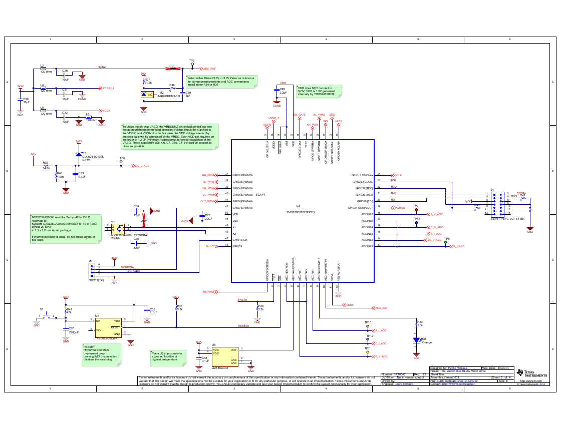
112233445566DDCCBBAA243/3/2014BLDC Standard sheet 2.SchDocSheet Title:Size:Mod. Date:File:Sheet:ofBhttp://www.ti.comContact:http://www.ti.com/supportAutomotive BLDC Motor DriveProject Title:Designed for:Public ReleaseAssembly Variant:001© Texas Instruments2014Drawn By:Engineer:Clark KinnairdTexas Instruments and/or its licensors do not warrant the accuracy or completeness of this specification or any information contained therein. Texas Instruments and/or its licensors do not warrant that this design will meet the specifications, will be suitable for your application or fit for any particular purpose, or will operate in an implementation. Texas Instruments and/or its licensors do not warrant that the design is production worthy. You should completely validate and test your design implementation to confirm the system functionality for your application.Not in version controlSVN Rev:SAT0042Number:Rev:E510µFC3110µFC32DGNDGND3p3VVDDIO_2VDDAVDDA1342GG20MHzY1NX3225GA20MHZSTDCRA1SCLKAH_PWMAL_PWMBH_PWMBL_PWMDGNDPWRGDDGND3p3V2.2kR46GND2.2kR45DC+34.8kR394.99kR40GNDDC_V_ADC0.44VD5CD0603-B0130L3p3V10µFC30GND12pFC3512pFC34GNDGND2.2µFC280.1µFC33GPIO29/SCITXDA1TRST2XRS3ADCIND6/AIO64ADCINA4/COMP2A5ADCINA76ADCINA37ADCINA18ADCINA2/COMP1A9ADCINA0/VREFHI10VDDA11VSSA/VREFLO12ADCINB113ADCINB214ADCINB315ADCINB416ADCINB617ADCINB718GPIO34,COMP2OUT19GPIO35,[TDI]20GPIO36,[TMS]21GPIO37,[TDO]22GPIO38,XCLKIN,23GPIO18,SPICLKA24GPIO19,XCLKIN25GPIO17,SPISOMIA,26GPIO16,SPISIMOA27GPIO1,EPWM1B28GPIO0,EPWM1A29TEST30GPIO32,SDAA31VDD32VSS33VREGENZ34VDDIO35GPIO33,SCLA36GPIO2,EPWM2A37GPIO3,EPWM2B38GPIO4,EPWM3A39GPIO5,EPWM3B40GPIO6,EPWM4A41GPIO7,EPWM4B42VDD43VSS44X145X246GPIO12,TZ147GPIO2848U3TMS320F28027FPTQGNDVDDIO_2DGNDTDITDOTMSTCKRESETnTRSTnGND1GND2OUT3VDD4VDD5U5LMT86DCKT10µFC26GNDGND3p3V0.1µFC38GND1µFC29DC+NCU2LM4040DEM3-3.031.6kR37GND0R380R36DNPADC_REFECAP1TP5TP61.0kR43GNDTRSTn21S1GNDGND3p3V2200pFC371234567891011121314J4SBH11-PBPC-D07-ST-BK3p3V0R42GND0R41TDIS120 ohmL2120 ohmL4120 ohmL5120 ohmL63p3refRESET1GND2MR3WDI4VDD5U4TPS3828-33DBVGND0.1µFC36GND47kR470R71DNPCH_PWMCL_PWMOrange12D8ADC_REFA_I_ADCTP10B_V_ADCTP7B_I_ADCTP8A_I_ADCA_V_ADCTP9C_I_ADCTP12DC_V_ADCC_V_ADCTP11SDOSDIFAULTEN_GATEOUT_PWM4123J500221120423p3VGNDSCIRXDASCITXDAnSCSIN_PWMOCTWVDDNX3225GA20000 rated for Temp -40 to 150 CAlternate is:Kyocera CX3225CA20000D0HSSZ1 is -40 to 125C crystal 20 MHzin 2.5 x 3.2 mm 4 pad packageIf internal oscillator is used, do not install crystal or two caps.To utilize the on-chip VREG, the VREGENZ pin should be tied low and the appropriate recommended operating voltage should be supplied to the VDDIO and VDDA pins. In this case, the VDD voltage needed bythe core logic will be generated by the VREG. Each VDD pin requires on the order of 1.2 µF (minimum) capacitance for proper regulation of the VREG. These capacitors (C5, C6, C7, C10, C11) should be located as close as possibleto the VDD pins.Place U3 in proximity to expected location of highest temperature.Select either filtered 3.3V or 3.0V Zener as reference for current measurements and ADC conversions.Install either R34 or R36nRESETH=normal operationL=powered downLeaving WDI unconnected disables the watchdogVDD does NOT connect to 3p3V; VDD is 1.8V generated internally by TMS320F280352.2µFC27�
PIR4902
PIR4902
COR49
PIR4901
PIR4901
PIR5002
PIR5002
COR50
PIR5001
PIR5001
PIC4401
PIC4401
PIC4402
PIC4402
COC44
PIC4201
PIC4201
PIC4202
PIC4202
COC42
COR53
COR55
PIR5302
PIR5302
PIR5301
PIR5301
PIR5502
PIR5502
PIR5501
PIR5501
NLDRV0RT0CLK
NLDRV0COMP
NLDRV0VSENSE
NLPWRGD
COR52
PIR5201
PIR5201
PIR5202
PIR5202
COR54
PIR5401
PIR5401
PIR5402
PIR5402
COU6
PIU601
PIU601
PIU602
PIU602
PIU603
PIU603
PIU604
PIU604
PIU605
PIU605
PIU606
PIU606
COR56
PIR5601
PIR5601
PIR5602
PIU607
PIR5602 PIU607
COR59
PIR5901
PIR5901
PIR5902
PIR5902
COR60
PIR6001
PIR6001
PIR6002
PIR6002
COC48
PIC4802
PIC4802
PIC4801
PIC4801
PIC5001
PIC5001
PIC5002
PIC5002
COC50
PIR6102
PIR6102
COR61
PIR6101
PIR6101
PIC5201
PIC5201
PIC5202
PIC5202
COC52
PIC5301
PIC5301
PIC5302
PIC5302
COC53
PIC5401
PIC5401
PIC5402
PIC5402
COC54
PIC5501
PIC5501
PIC5502
PIC5502
COC55
PIC5601
PIC5601
PIC5602
PIC5602
COC56
PIU608
PIU608
PIU609
PIU609
PIU6010
PIU6010
PIU6011
PIU6011
PIU6012
PIU6012
PIU6013
PIU6013
PIU6014
PIU6014
PIU6015
PIU6015
PIU6016
PIU6016
PIU6017
PIU6017
PIU6018
PIU6018
PIU6019
PIU6019
PIU6020
PIU6020
PIU6021
PIU6021
PIU6022
PIU6022
PIU6023
PIU6023
PIU6024
PIU6024
PIU6025
PIU6025
PIU6026
PIU6026
PIU6027
PIU6027
PIU6028
PIU6028
PIU6057
PIU6057
COC61
PIC6101
PIC6101
PIC6102
PIC6102
PIU708
PIU708
PIU707
PIU707
PIU706
PIU706
PIU705
PIU705
COU7
PIU701
PIU701
PIU702
PIU702
PIU703
PIU703
PIU704
PIU704
COR69
PIR6901
PIR6901
PIR6902
PIR6902
COR70
PIR7001
PIR7001
PIR7002
PIR7002
COC66
PIC6601
PIC6601
PIC6602
PIC6602
PIR6502
PIR6502
COR65
PIR6501
PIR6501
PIR6701
PIR6701
COR67
PIR6702
PIR6702
NLHalf0REF
PIC6301
PIC6301
PIC6302
PIC6302
COC63
COR68
PIR6802
PIR6802
PIR6801
PIR6801
PIR4802
PIR4802
COR48
PIR4801
PIR4801
PIR5102
PIR5102
COR51
PIR5101
PIR5101
PIC4601
PIC4601
PIC4602
PIC4602
COC46
COL7
PIL701
PIL701
PIL702
PIL702
PID701
PID701
PID702
PID702
COD7
PIC4501
PIC4501
PIC4502
PIC4502
COC45
PIR5802
PIR5802
COR58
PIR5801
PIR5801
PID601
PID601
PID602
PID602
COD6
PIU6056
PIU6056
PIU6055
PIU6055
PIU6054
PIU6054
PIU6053
PIU6053
PIU6052
PIU6052
PIU6051
PIU6051
PIU6050
PIU6050
PIU6049
PIU6049
PIU6048
PIU6048
PIU6047
PIU6047
PIU6046
PIU6046
PIU6045
PIU6045
PIU6044
PIU6044
PIU6043
PIU6043
PIU6042
PIU6042
PIU6041
PIU6041
PIU6040
PIU6040
PIU6039
PIU6039
PIU6038
PIU6038
PIU6037
PIU6037
PIU6036
PIU6036
PIU6035
PIU6035
PIU6034
PIU6034
PIU6033
PIU6033
PIU6032
PIU6032
PIU6031
PIU6031
PIU6030
PIU6030
PIU6029
PIU6029
COC39
PIC3901
PIC3901
PIC4001
PIC4001
PIC4002
PIC4002
COC40
PIC4101
PIC4101
PIC4102
PIC4102
COC41
NLDRV0SS0TR
PIC3902
PIC3902
COC43
PIC4302
PIC4302
PIC4301
PIC4301
COC47
PIC4701
PIC4701
PIC4702
PIC4702
COC49
PIC4901
PIC4901
PIC4902
PIC4902
COC51
PIC5101
PIC5101
PIC5102
PIC5102
COC64
PIC6401
PIC6401
PIC6402
PIC6402
COC65
PIC6501
PIC6501
PIC6502
PIC6502
PIC5701
PIC5701
PIC5702
PIC5702
COC57
PIC5801
PIC5801
PIC5802
PIC5802
COC58
COR62
PIR6201
PIR6201
PIR6202
PIR6202
PIC5901
PIC5901
PIC5902
PIC5902
COC59
COR63
PIR6301
PIR6301
PIR6302
PIR6302
PIC6001
PIC6001
PIC6002
PIC6002
COC60
COR64
PIR6401
PIR6401
PIR6402
PIR6402
PIC6201
PIC6201
PIC6202
PIC6202
COC62
PIR6602
PIR6602
COR66
PIR6601
PIR6601
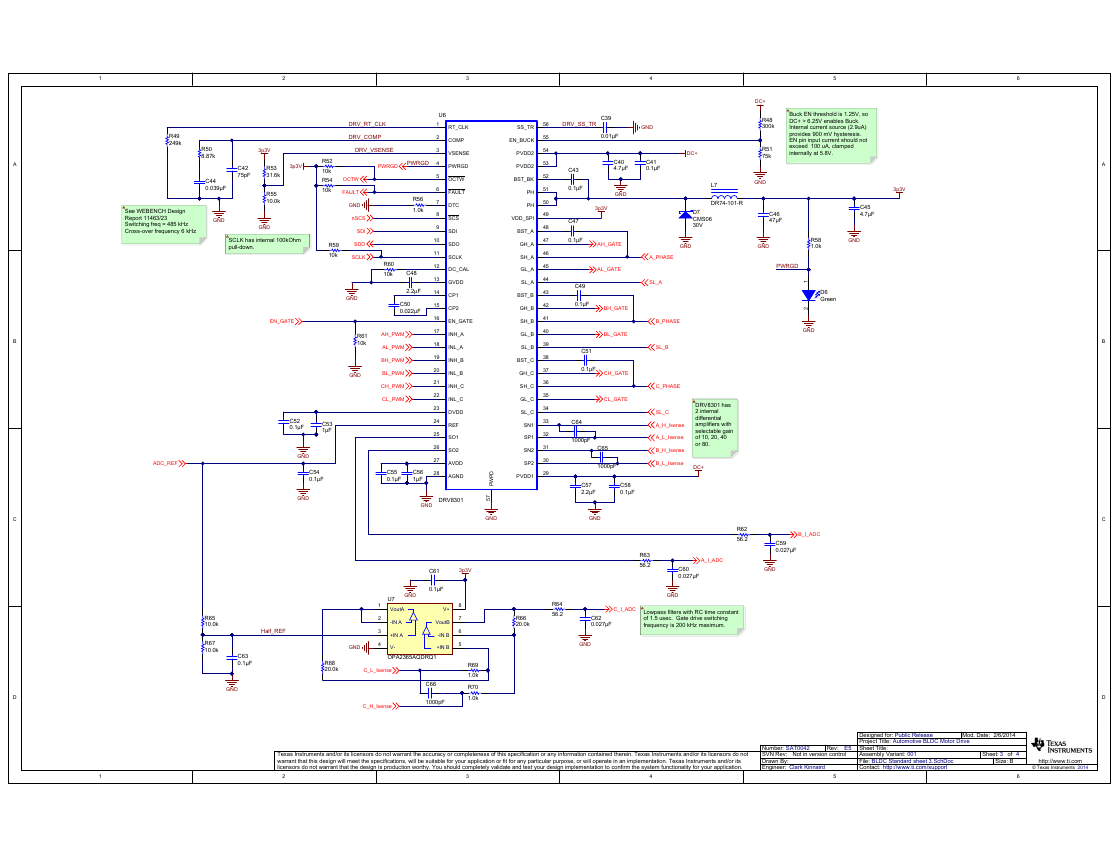
112233445566DDCCBBAA342/6/2014BLDC Standard sheet 3.SchDocSheet Title:Size:Mod. Date:File:Sheet:ofBhttp://www.ti.comContact:http://www.ti.com/supportAutomotive BLDC Motor DriveProject Title:Designed for:Public ReleaseAssembly Variant:001© Texas Instruments2014Drawn By:Engineer:Clark KinnairdTexas Instruments and/or its licensors do not warrant the accuracy or completeness of this specification or any information contained therein. Texas Instruments and/or its licensors do not warrant that this design will meet the specifications, will be suitable for your application or fit for any particular purpose, or will operate in an implementation. Texas Instruments and/or its licensors do not warrant that the design is production worthy. You should completely validate and test your design implementation to confirm the system functionality for your application.Not in version controlSVN Rev:SAT0042Number:Rev:E5B_I_ADCA_H_IsenseA_L_IsenseB_H_IsenseB_L_IsenseSL_ASL_BSL_CGND10.0kR55GND3p3VGND0.1µFC41GND0.1µFC43RT_CLK1COMP2VSENSE3PWRGD4OCTW5FAULT6DTC7SCS8SDI9SDO10SCLK11DC_CAL12GVDD13CP114CP215EN_GATE16INH_A17INL_A18INH_B19INL_B20INH_C21INL_C22DVDD23REF24SO125SO226AVDD27AGND28PVDD129SP230SN231SP132SN133SL_C34GL_C35SH_C36GH_C37BST_C38SL_B39GL_B40SH_B41GH_B42BST_B43SL_A44GL_A45SH_A46GH_A47BST_A48VDD_SPI49PH50PH51BST_BK52PVDD253PVDD254EN_BUCK55SS_TR56PWPD57U6DRV8301OCTWFAULT1.0kR56SDISDOSCLKGND0.022µFC50EN_GATEGNDAH_PWMAL_PWMBH_PWMBL_PWMCH_PWMCL_PWMGNDGNDA_I_ADCGND0.1µFC58GNDCL_GATEC_PHASECH_GATE0.1µFC51BL_GATEB_PHASEBH_GATE0.1µFC49AL_GATEA_PHASE0.1µFC47AH_GATE3p3VDC+DC+GND0.1µFC520.1µFC553p3VDRV_SS_TRDRV_COMPDRV_VSENSEGNDGND3p3V249kR49GNDDRV_RT_CLKGNDGND1µFC564.7µFC402.2µFC482.2µFC5747µFC4656.2R6256.2R630.027µFC590.027µFC60GNDGNDPWRGDPWRGDPWRGD4.7µFC45GND30VD7CMS0631.6kR530.01µFC39ADC_REF0.1µFC54DC+3p3VGNDGNDC_I_ADCC_L_IsenseC_H_IsenseVoutA1-IN A2+IN A3V-4+IN B5-IN B6VoutB7V+8U7OPA2365AQDRQ11.0kR701.0kR6920.0kR6856.2R640.027µFC620.1µFC6310.0kR65GND10.0kR6720.0kR66Half_REFL7DR74-101-R8.87kR500.039µFC4475pFC421µFC5310kR5210kR5410kR59300kR4875kR510.1µFC61GND1.0kR5810kR61Green12D610kR60nSCS1000pFC641000pFC651000pFC66Buck EN threshold is 1.25V, so DC+ > 6.25V enables Buck.Internal current source (2.9uA) provides 900 mV hysteresis.EN pin input current should not exceed 100 uA, clamped internally at 5.8V.See WEBENCH Design Report 11463/23Switching freq = 485 kHzCross-over frequency 6 kHzSCLK has internal 100kOhm pull-down.DRV8301 has 2 internal differential amplifiers with selectable gain of 10, 20, 40 or 80.Lowpass filters with RC time constant of 1.5 usec. Gate drive switching frequency is 200 kHz maximum.�
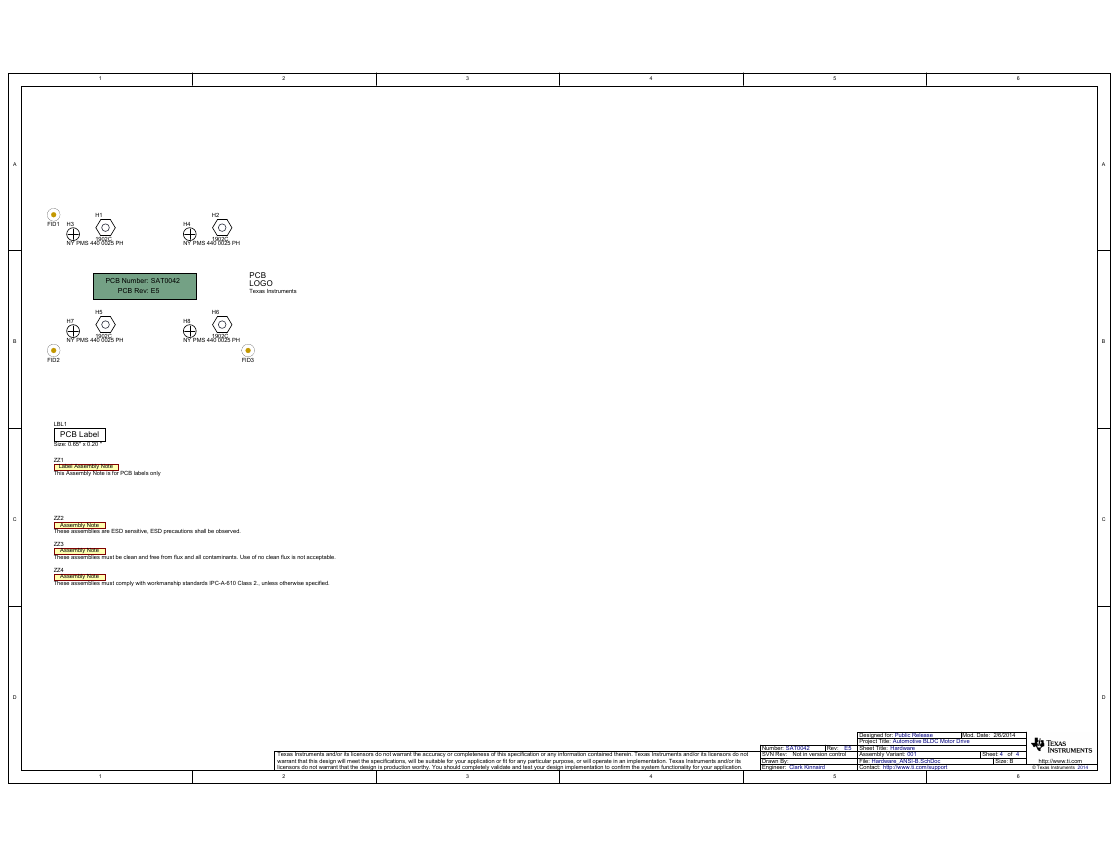
112233445566DDCCBBAA44Hardware2/6/2014Hardware_ANSI-B.SchDocSheet Title:Size:Mod. Date:File:Sheet:ofBhttp://www.ti.comContact:http://www.ti.com/supportAutomotive BLDC Motor DriveProject Title:Designed for:Public ReleaseAssembly Variant:001© Texas Instruments2014Drawn By:Engineer:Clark KinnairdTexas Instruments and/or its licensors do not warrant the accuracy or completeness of this specification or any information contained therein. Texas Instruments and/or its licensors do not warrant that this design will meet the specifications, will be suitable for your application or fit for any particular purpose, or will operate in an implementation. Texas Instruments and/or its licensors do not warrant that the design is production worthy. You should completely validate and test your design implementation to confirm the system functionality for your application.Not in version controlSVN Rev:SAT0042Number:Rev:E5LOGOPCBTexas InstrumentsH3NY PMS 440 0025 PHH4NY PMS 440 0025 PHH7NY PMS 440 0025 PHH8NY PMS 440 0025 PHH11902CH21902CH51902CH61902CFID2FID1FID3SAT0042E5PCB Number:PCB Rev:Label Assembly NoteZZ1This Assembly Note is for PCB labels onlyPCB LabelLBL1Size: 0.65" x 0.20 "Assembly NoteZZ2These assemblies are ESD sensitive, ESD precautions shall be observed.Assembly NoteZZ3These assemblies must be clean and free from flux and all contaminants. Use of no clean flux is not acceptable.Assembly NoteZZ4These assemblies must comply with workmanship standards IPC-A-610 Class 2., unless otherwise specified.�
COC8
PIC801
PIC801
PIC802
PIC802
COC11
PIC1102
PIC1102
PIC1101
PIC1101
COR15
PIR1501
PIR1501
PIR1502
PIR1502
PIC1401
PIC1401
PIC1402
PIC1402
COC14
COR18
PIR1801
PIR1801
PIR1802
PIR1802
PIQ204
PIQ204
COQ2
PIQ205
PIQ206
PIQ207
PIQ208
PIQ209
PIQ205
PIQ206
PIQ207
PIQ208
PIQ209
PIQ201
PIQ202
PIQ203
PIQ201
PIQ202
PIQ203
COPTH0A
PIPTH0A01
PIPTH0A01
COR21
PIR2101
PIR2101
PIR2102
PIR2102
PID201
PID201
PID202
PID202
COD2
PIR2402
PIR2402
COR24
PIR2401
PIR2401
PIC1701
PIC1701
PIC1702
PIC1702
COC17
COC20
PIC2002
PIC2002
PIC2001
PIC2001
COR27
PIR2701
PIR2701
PIR2702
PIR2702
COR30
PIR3001
PIR3001
PIR3002
PIR3002
PIQ504
PIQ504
COQ5
PIQ505
PIQ506
PIQ507
PIQ508
PIQ509
PIQ505
PIQ506
PIQ507
PIQ508
PIQ509
PIQ501
PIQ502
PIQ503
PIQ501
PIQ502
PIQ503
COC23
PIC2301
PIC2301
PIC2302
PIC2302
COJ3
PIJ303
PIJ303
PIJ302
PIJ302
PIJ301
PIJ301
COC9
PIC901 PIC902
PIC901
PIC902
COC12
PIC1202
PIC1202
PIC1201
PIC1201
COR16
PIR1601
PIR1601
PIR1602
PIR1602
COR19
PIR1901
PIR1901
PIR1902
PIR1902
PIQ304
PIQ304
COC21
PIC2102
PIC2102
PIC2101
PIC2101
COR31
PIR3101
PIR3101
PIR3102
PIR3102
PIQ604
PIQ604
PIC1501
PIC1501
PIC1502
PIC1502
COC15
COQ3
COPTH0B
PIPTH0B01
PIPTH0B01
COR22
PIR2201
PIR2201
PIR2202
PIR2202
PID301
PID301
PID302
PID302
COD3
PIR2502
PIR2502
COR25
PIR2501
PIR2501
PIC1801
PIC1801
PIC1802
PIC1802
COC18
COR28
PIR2801
PIR2801
PIR2802
PIR2802
COQ6
PIC2401
PIC2401
PIC2402
PIC2402
COC24
PIQ305
PIQ306
PIQ307
PIQ308
PIQ309
PIQ305
PIQ306
PIQ307
PIQ308
PIQ309
PIQ301
PIQ302
PIQ303
PIQ301
PIQ302
PIQ303
PIQ605
PIQ606
PIQ607
PIQ608
PIQ609
PIQ605
PIQ606
PIQ607
PIQ608
PIQ609
PIQ601
PIQ602
PIQ603
PIQ601
PIQ602
PIQ603
COC10
PIC1001
PIC1001
PIC1002
PIC1002
COC13
PIC1302
PIC1302
PIC1301
PIC1301
COR17
PIR1701
PIR1701
PIR1702
PIR1702
PIC1601
PIC1601
PIC1602
PIC1602
COC16
COR20
PIR2001
PIR2001
PIR2002
PIR2002
PIQ404
PIQ404
COQ4
PIQ405
PIQ406
PIQ407
PIQ408
PIQ409
PIQ405
PIQ406
PIQ407
PIQ408
PIQ409
PIQ401
PIQ402
PIQ403
PIQ401
PIQ402
PIQ403
COPTH0C
PIPTH0C01
PIPTH0C01
COR23
PIR2301
PIR2301
PIR2302
PIR2302
PID401
PID401
PID402
PID402
COD4
COR26
PIR2602
PIR2602
PIR2601
PIR2601
PIC1901
PIC1901
PIC1902
PIC1902
COC19
COC22
PIC2202
PIC2202
PIC2201
PIC2201
COR29
PIR2901
PIR2901
PIR2902
PIR2902
COR32
PIR3201
PIR3201
PIR3202
PIR3202
PIQ704
PIQ704
COQ7
PIQ705
PIQ706
PIQ707
PIQ708
PIQ709
PIQ705
PIQ706
PIQ707
PIQ708
PIQ709
PIQ701
PIQ702
PIQ703
PIQ701
PIQ702
PIQ703
COC25
PIC2501
PIC2501
PIC2502
PIC2502
PIR3302
PIR3302
COR33
PIR3301
PIR3301
CONT1
PINT101
PINT101
PINT102
PINT102
CONT4
PINT401
PINT401
PINT402
PINT402
COR34
PIR3402
PIR3402
PIR3401
PIR3401
CONT2
PINT201
PINT201
PINT202
PINT202
CONT5
PINT501
PINT501
PINT502
PINT502
PIR3502
PIR3502
COR35
PIR3501
PIR3501
CONT3
PINT301
PINT301
PINT302
PINT302
CONT6
PINT601
PINT601
PINT602
PINT602
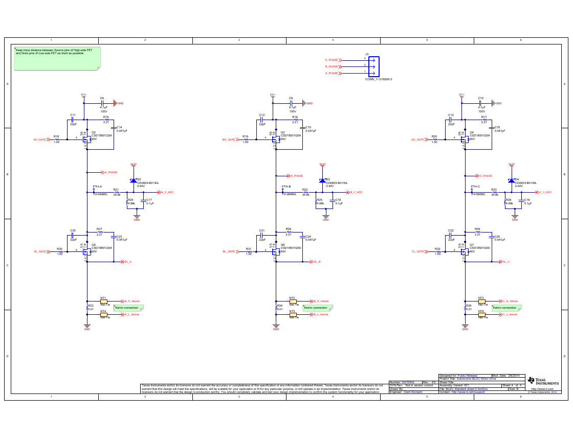
112233445566DDCCBBAA442/6/2014BLDC Standard sheet 4.SchDocSheet Title:Size:Mod. Date:File:Sheet:ofBhttp://www.ti.comContact:http://www.ti.com/supportAutomotive BLDC Motor DriveProject Title:Designed for:Public ReleaseAssembly Variant:001© Texas Instruments2014Drawn By:Engineer:Clark KinnairdTexas Instruments and/or its licensors do not warrant the accuracy or completeness of this specification or any information contained therein. Texas Instruments and/or its licensors do not warrant that this design will meet the specifications, will be suitable for your application or fit for any particular purpose, or will operate in an implementation. Texas Instruments and/or its licensors do not warrant that the design is production worthy. You should completely validate and test your design implementation to confirm the system functionality for your application.Not in version controlSVN Rev:SAT0042Number:Rev:E5DC+4.7µF100VC8GNDGNDA_H_IsenseA_L_IsenseAH_GATEAL_GATESL_A2.21R272.21R150.047µFC140.047µFC2322pFC1122pFC201.00R181.00R30NT4Net-TieNT1Net-Tie47,81,2,35,6,40VQ5CSD18501Q5A47,81,2,35,6,40VQ2CSD18501Q5A34.8kR214.99kR24GNDA_V_ADC0.44VD2CD0603-B0130L3p3V0.1µFC17PTH-ATH-094MILDC+4.7µF100VC9GNDGNDB_H_IsenseB_L_IsenseBH_GATEBL_GATESL_B2.21R282.21R160.047µFC150.047µFC2422pFC1222pFC211.00R191.00R31NT5Net-TieNT2Net-Tie47,81,2,35,6,40VQ6CSD18501Q5A47,81,2,35,6,40VQ3CSD18501Q5A34.8kR224.99kR25GNDB_V_ADC0.44VD3CD0603-B0130L3p3V0.1µFC18PTH-BTH-094MILDC+4.7µF100VC10GNDGNDC_H_IsenseC_L_IsenseCH_GATECL_GATESL_C2.21R292.21R170.047µFC160.047µFC2522pFC1322pFC221.00R201.00R32NT6Net-TieNT3Net-Tie47,81,2,35,6,40VQ7CSD18501Q5A47,81,2,35,6,40VQ4CSD18501Q5A34.8kR234.99kR26GNDC_V_ADC0.44VD4CD0603-B0130L3p3V0.1µFC19PTH-CTH-094MIL123J3CONN_1-1318300-30.01R330.01R340.01R35A_PHASEB_PHASEC_PHASEC_PHASEB_PHASEA_PHASEKelvin connectionKeep trace distance between Source pins of High-side FET and Drain pins of Low-side FET as short as possible.Kelvin connectionKelvin connection�
IMPORTANT NOTICE
Texas Instruments Incorporated and its subsidiaries (TI) reserve the right to make corrections, enhancements, improvements and other
changes to its semiconductor products and services per JESD46, latest issue, and to discontinue any product or service per JESD48, latest
issue. Buyers should obtain the latest relevant information before placing orders and should verify that such information is current and
complete. All semiconductor products (also referred to herein as “components”) are sold subject to TI’s terms and conditions of sale
supplied at the time of order acknowledgment.
TI warrants performance of its components to the specifications applicable at the time of sale, in accordance with the warranty in TI’s terms
and conditions of sale of semiconductor products. Testing and other quality control techniques are used to the extent TI deems necessary
to support this warranty. Except where mandated by applicable law, testing of all parameters of each component is not necessarily
performed.
TI assumes no liability for applications assistance or the design of Buyers’ products. Buyers are responsible for their products and
applications using TI components. To minimize the risks associated with Buyers’ products and applications, Buyers should provide
adequate design and operating safeguards.
TI does not warrant or represent that any license, either express or implied, is granted under any patent right, copyright, mask work right, or
other intellectual property right relating to any combination, machine, or process in which TI components or services are used. Information
published by TI regarding third-party products or services does not constitute a license to use such products or services or a warranty or
endorsement thereof. Use of such information may require a license from a third party under the patents or other intellectual property of the
third party, or a license from TI under the patents or other intellectual property of TI.
Reproduction of significant portions of TI information in TI data books or data sheets is permissible only if reproduction is without alteration
and is accompanied by all associated warranties, conditions, limitations, and notices. TI is not responsible or liable for such altered
documentation. Information of third parties may be subject to additional restrictions.
Resale of TI components or services with statements different from or beyond the parameters stated by TI for that component or service
voids all express and any implied warranties for the associated TI component or service and is an unfair and deceptive business practice.
TI is not responsible or liable for any such statements.
Buyer acknowledges and agrees that it is solely responsible for compliance with all legal, regulatory and safety-related requirements
concerning its products, and any use of TI components in its applications, notwithstanding any applications-related information or support
that may be provided by TI. Buyer represents and agrees that it has all the necessary expertise to create and implement safeguards which
anticipate dangerous consequences of failures, monitor failures and their consequences, lessen the likelihood of failures that might cause
harm and take appropriate remedial actions. Buyer will fully indemnify TI and its representatives against any damages arising out of the use
of any TI components in safety-critical applications.
In some cases, TI components may be promoted specifically to facilitate safety-related applications. With such components, TI’s goal is to
help enable customers to design and create their own end-product solutions that meet applicable functional safety standards and
requirements. Nonetheless, such components are subject to these terms.
No TI components are authorized for use in FDA Class III (or similar life-critical medical equipment) unless authorized officers of the parties
have executed a special agreement specifically governing such use.
Only those TI components which TI has specifically designated as military grade or “enhanced plastic” are designed and intended for use in
military/aerospace applications or environments. Buyer acknowledges and agrees that any military or aerospace use of TI components
which have not been so designated is solely at the Buyer's risk, and that Buyer is solely responsible for compliance with all legal and
regulatory requirements in connection with such use.
TI has specifically designated certain components as meeting ISO/TS16949 requirements, mainly for automotive use. In any case of use of
non-designated products, TI will not be responsible for any failure to meet ISO/TS16949.
Products
Audio
Amplifiers
Data Converters
DLP® Products
DSP
Clocks and Timers
Interface
Logic
Power Mgmt
Microcontrollers
RFID
OMAP Applications Processors
Wireless Connectivity
Applications
Automotive and Transportation www.ti.com/automotive
Communications and Telecom www.ti.com/communications
Computers and Peripherals
Consumer Electronics
Energy and Lighting
Industrial
Medical
Security
Space, Avionics and Defense
Video and Imaging
www.ti.com/audio
amplifier.ti.com
dataconverter.ti.com
www.dlp.com
dsp.ti.com
www.ti.com/clocks
interface.ti.com
logic.ti.com
power.ti.com
microcontroller.ti.com
www.ti-rfid.com
www.ti.com/omap
www.ti.com/wirelessconnectivity
www.ti.com/computers
www.ti.com/consumer-apps
www.ti.com/energy
www.ti.com/industrial
www.ti.com/medical
www.ti.com/security
www.ti.com/space-avionics-defense
www.ti.com/video
TI E2E Community
e2e.ti.com
Mailing Address: Texas Instruments, Post Office Box 655303, Dallas, Texas 75265
Copyright © 2014, Texas Instruments Incorporated
�



 2023年江西萍乡中考道德与法治真题及答案.doc
 2012年重庆南川中考生物真题及答案.doc
 2013年江西师范大学地理学综合及文艺理论基础考研真题.doc
 2020年四川甘孜小升初语文真题及答案I卷.doc
 2020年注册岩土工程师专业基础考试真题及答案.doc
 2023-2024学年福建省厦门市九年级上学期数学月考试题及答案.doc
 2021-2022学年辽宁省沈阳市大东区九年级上学期语文期末试题及答案.doc
 2022-2023学年北京东城区初三第一学期物理期末试卷及答案.doc
 2018上半年江西教师资格初中地理学科知识与教学能力真题及答案.doc
 2012年河北国家公务员申论考试真题及答案-省级.doc
 2020-2021学年江苏省扬州市江都区邵樊片九年级上学期数学第一次质量检测试题及答案.doc
 2022下半年黑龙江教师资格证中学综合素质真题及答案.doc