PCIe® 2.0 Compliance Testing
PCIe® 2.0 Compliance Testing
Betty Luk
Betty Luk
AMD
AMD
Serial Enabling Workgroup Co-Chair
Serial Enabling Workgroup Co-Chair
1
�
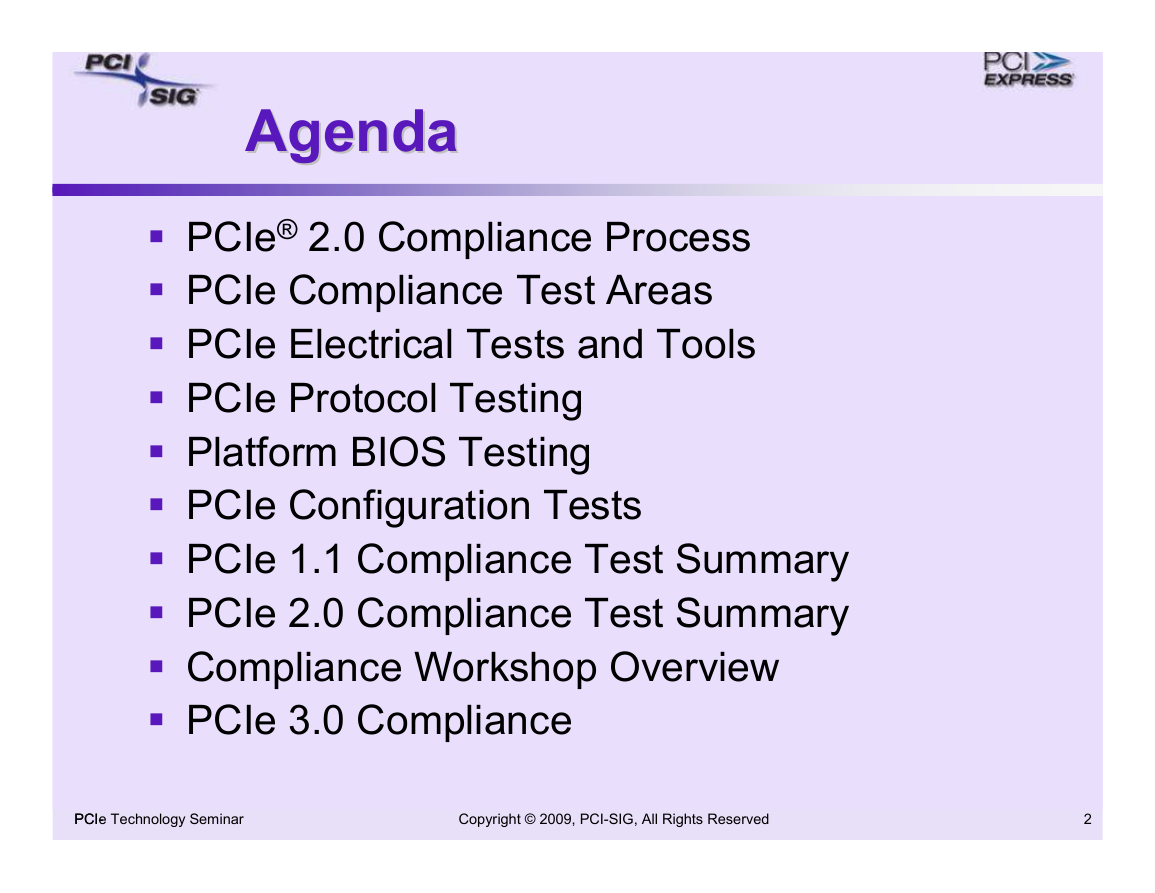
Agenda
Agenda
� PCIe® 2.0 Compliance Process
� PCIe Compliance Test Areas
� PCIe Electrical Tests and Tools
� PCIe Protocol Testing
� Platform BIOS Testing
� PCIe Configuration Tests
� PCIe 1.1 Compliance Test Summary
� PCIe 2.0 Compliance Test Summary
� Compliance Workshop Overview
� PCIe 3.0 Compliance
PCIe Technology Seminar
PCI-
Copyright © 2009, PCI-SIG, All Rights Reserved
2
�
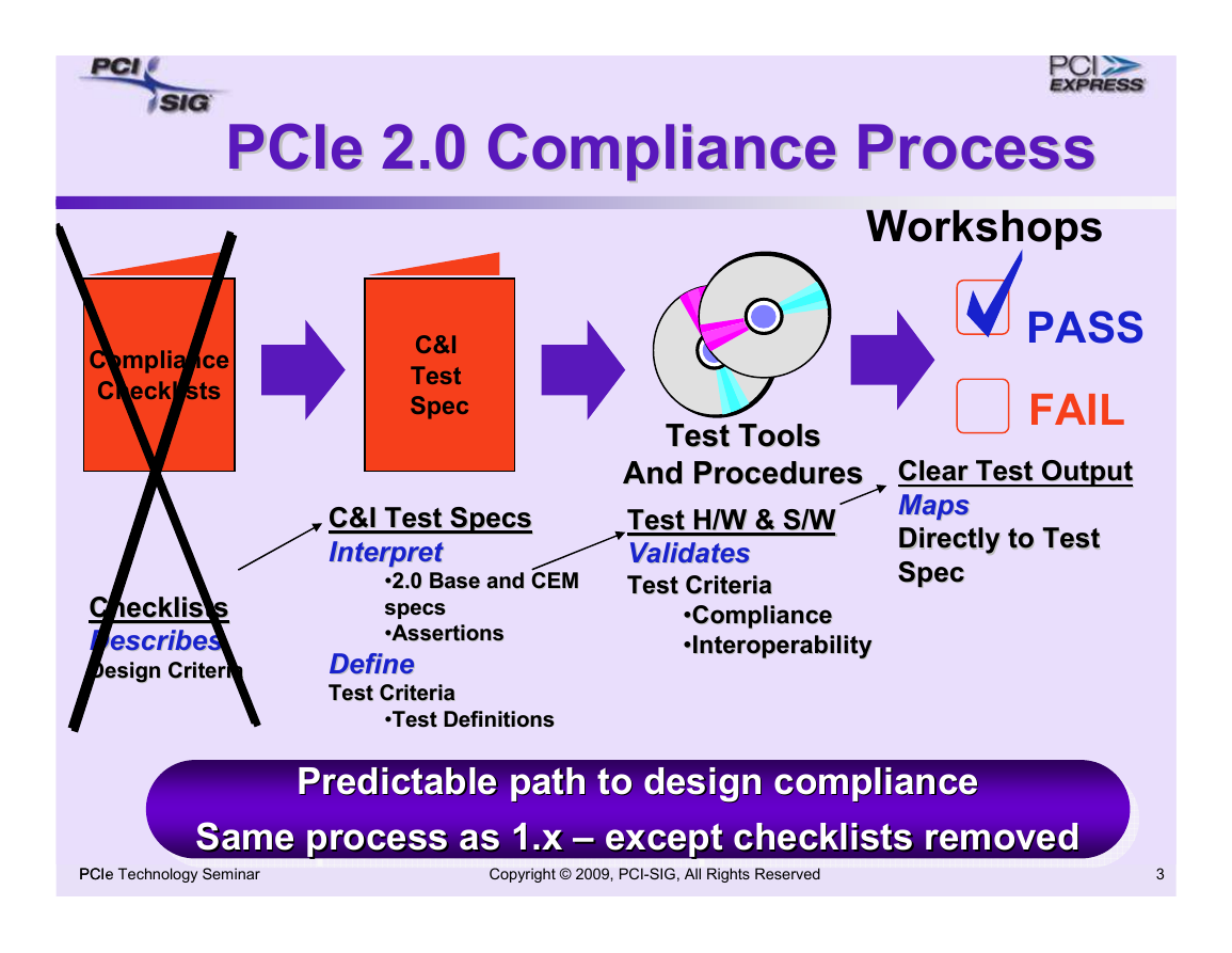
PCIe 2.0 Compliance Process
PCIe 2.0 Compliance Process
Workshops
Compliance
Checklists
C&I
Test
Spec
Checklists
Checklists
Describes
Describes
Design Criteria
Design Criteria
C&I Test Specs
C&I Test Specs
Interpret
Interpret
2.0 Base and CEM
••2.0 Base and CEM
specs
specs
Assertions
••Assertions
Define
Define
Test Criteria
Test Criteria
Test Definitions
••Test Definitions
PASS
FAIL
Clear Test Output
Clear Test Output
MapsMaps
Directly to Test
Directly to Test
SpecSpec
Test Tools
Test Tools
And Procedures
And Procedures
Test H/W & S/W
Test H/W & S/W
Validates
Validates
Test Criteria
Test Criteria
Compliance
••Compliance
Interoperability
••Interoperability
Predictable path to design compliance
Predictable path to design compliance
Predictable path to design compliance
Same process as 1.x –– except checklists removed
except checklists removed
Same process as 1.x
Same process as 1.x – except checklists removed
PCIe Technology Seminar
PCI-
Copyright © 2009, PCI-SIG, All Rights Reserved
3
�
PCI Express 2.0
PCI Express 2.0
Integrators List Status
Integrators List Status
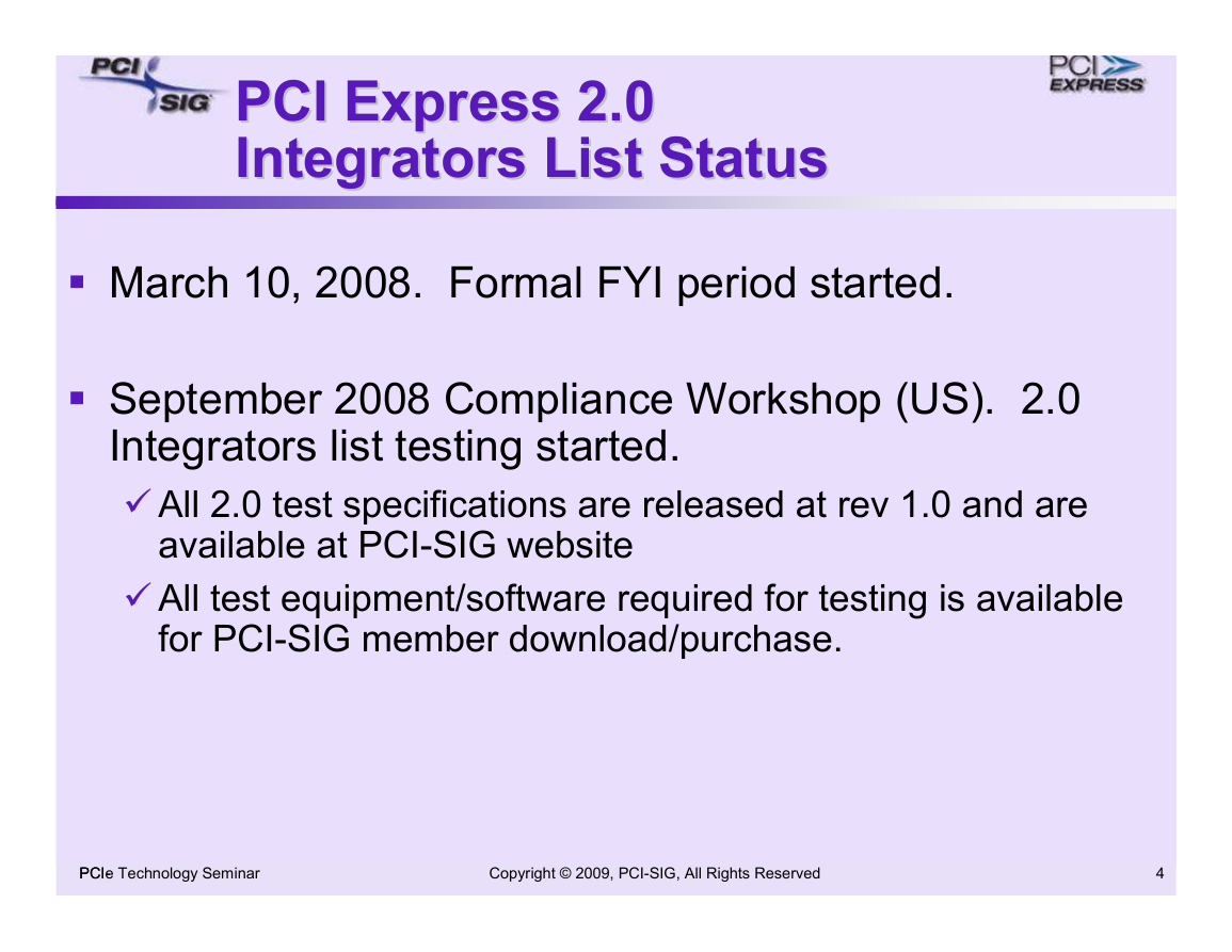
� March 10, 2008. Formal FYI period started.
� September 2008 Compliance Workshop (US). 2.0
Integrators list testing started.
All 2.0 test specifications are released at rev 1.0 and are
available at PCI-SIG website
All test equipment/software required for testing is available
for PCI-SIG member download/purchase.
PCIe Technology Seminar
PCI-
Copyright © 2009, PCI-SIG, All Rights Reserved
4
�
PCIe 1.1 Compliance Test Areas
PCIe 1.1 Compliance Test Areas
� Physical layer
Examine electrical signaling
� Configuration Space
Verify required fields and values
� Link & Transaction layer
Exercise protocol boundary conditions
Inject errors and check error handling
Available
Available
on PCISIG
on PCISIG
website
website
� Platform Configuration
Check BIOS handling of PCI Express devices
PCIe Technology Seminar
PCI-
Copyright © 2009, PCI-SIG, All Rights Reserved
5
�
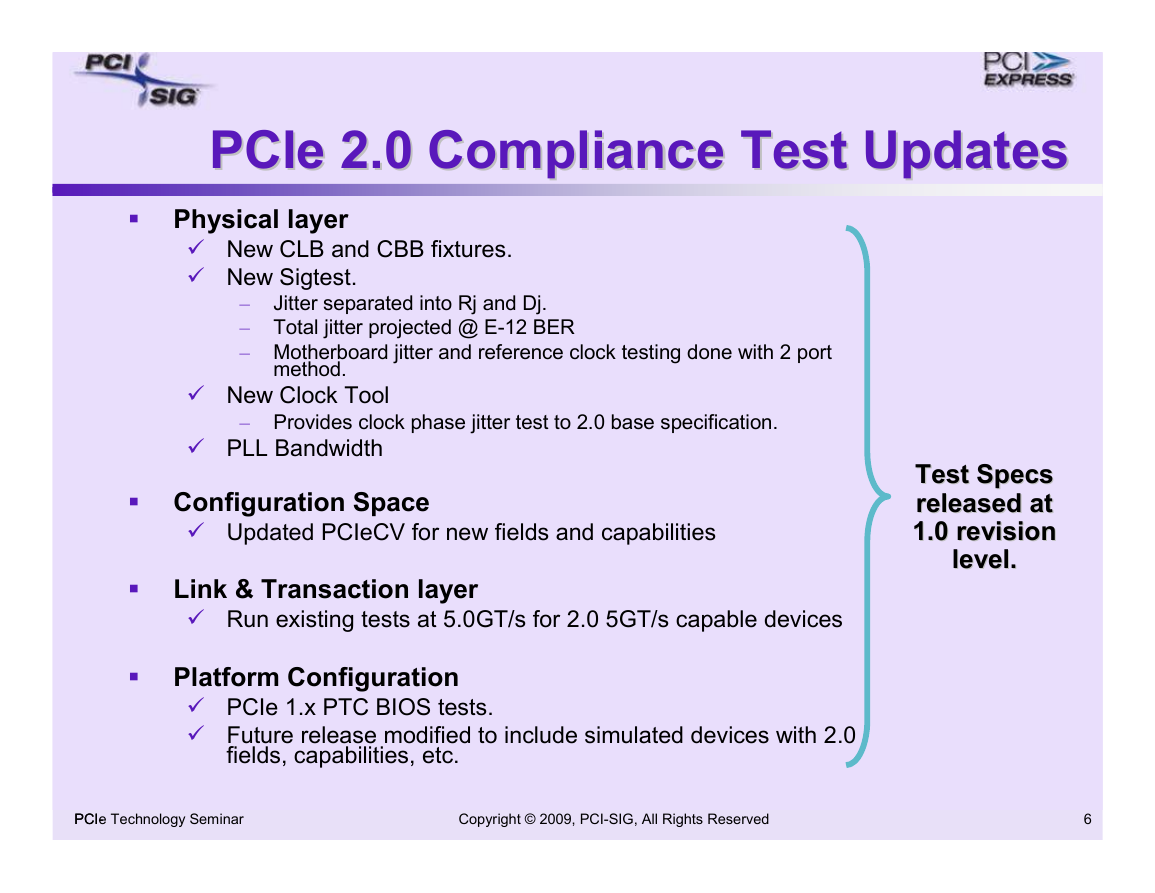
PCIe 2.0 Compliance Test Updates
PCIe 2.0 Compliance Test Updates
� Physical layer
New CLB and CBB fixtures.
New Sigtest.
Jitter separated into Rj and Dj.
–
– Total jitter projected @ E-12 BER
– Motherboard jitter and reference clock testing done with 2 port
method.
New Clock Tool
– Provides clock phase jitter test to 2.0 base specification.
PLL Bandwidth
� Configuration Space
Updated PCIeCV for new fields and capabilities
�
Link & Transaction layer
Run existing tests at 5.0GT/s for 2.0 5GT/s capable devices
� Platform Configuration
PCIe 1.x PTC BIOS tests.
Future release modified to include simulated devices with 2.0
fields, capabilities, etc.
Test Specs
Test Specs
released at
released at
1.0 revision
1.0 revision
level.
level.
PCIe Technology Seminar
PCI-
Copyright © 2009, PCI-SIG, All Rights Reserved
6
�
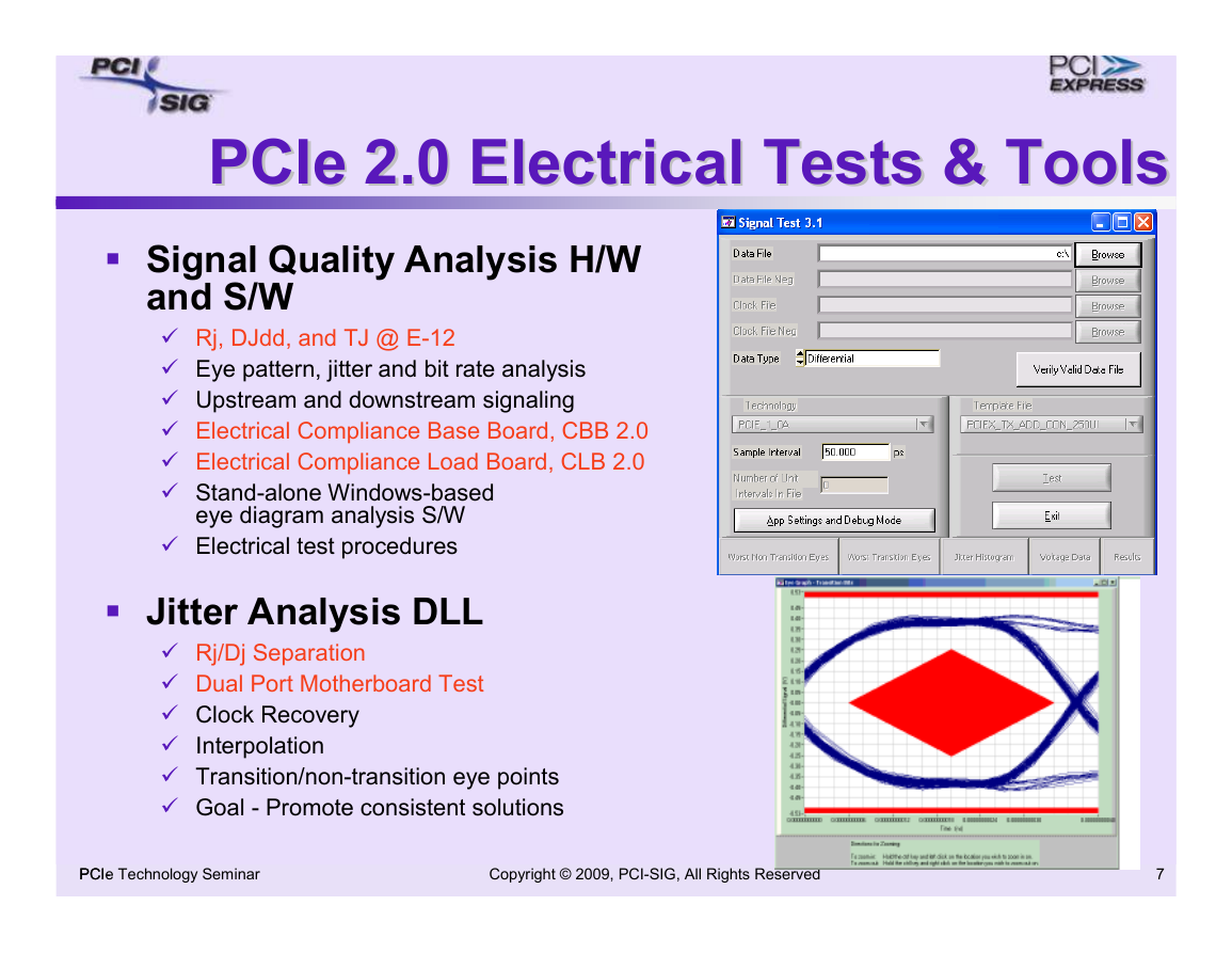
PCIe 2.0 Electrical Tests & Tools
PCIe 2.0 Electrical Tests & Tools
� Signal Quality Analysis H/W
and S/W
Rj, DJdd, and TJ @ E-12
Eye pattern, jitter and bit rate analysis
Upstream and downstream signaling
Electrical Compliance Base Board, CBB 2.0
Electrical Compliance Load Board, CLB 2.0
Stand-alone Windows-based
eye diagram analysis S/W
Electrical test procedures
� Jitter Analysis DLL
Rj/Dj Separation
Dual Port Motherboard Test
Clock Recovery
Interpolation
Transition/non-transition eye points
Goal - Promote consistent solutions
PCIe Technology Seminar
PCI-
Copyright © 2009, PCI-SIG, All Rights Reserved
7
�
PCIe 2.0 Motherboard
PCIe 2.0 Motherboard
Electrical Tools
Electrical Tools
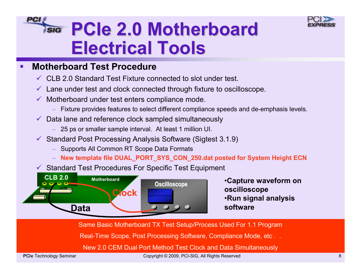
� Motherboard Test Procedure
CLB 2.0 Standard Test Fixture connected to slot under test.
Lane under test and clock connected through fixture to oscilloscope.
Motherboard under test enters compliance mode.
– Fixture provides features to select different compliance speeds and de-emphasis levels.
Data lane and reference clock sampled simultaneously
– 25 ps or smaller sample interval. At least 1 million UI.
Standard Post Processing Analysis Software (Sigtest 3.1.9)
– Supports All Common RT Scope Data Formats
– New template file DUAL_PORT_SYS_CON_250.dat posted for System Height ECN
Standard Test Procedures For Specific Test Equipment
CLB 2.0
Motherboard
Oscilloscope
Oscilloscope
Clock
Data
•Capture waveform on
oscilloscope
•Run signal analysis
software
Same Basic Motherboard TX Test Setup/Process Used For 1.1 Program
Real-Time Scope, Post Processing Software, Compliance Mode, etc . .
New 2.0 CEM Dual Port Method Test Clock and Data Simultaneously
PCIe Technology Seminar
PCI-
Copyright © 2009, PCI-SIG, All Rights Reserved
8
�



 2023年江西萍乡中考道德与法治真题及答案.doc
 2012年重庆南川中考生物真题及答案.doc
 2013年江西师范大学地理学综合及文艺理论基础考研真题.doc
 2020年四川甘孜小升初语文真题及答案I卷.doc
 2020年注册岩土工程师专业基础考试真题及答案.doc
 2023-2024学年福建省厦门市九年级上学期数学月考试题及答案.doc
 2021-2022学年辽宁省沈阳市大东区九年级上学期语文期末试题及答案.doc
 2022-2023学年北京东城区初三第一学期物理期末试卷及答案.doc
 2018上半年江西教师资格初中地理学科知识与教学能力真题及答案.doc
 2012年河北国家公务员申论考试真题及答案-省级.doc
 2020-2021学年江苏省扬州市江都区邵樊片九年级上学期数学第一次质量检测试题及答案.doc
 2022下半年黑龙江教师资格证中学综合素质真题及答案.doc