Henry Ott Consultants
http://www.hottconsultants.com/index.html
PCB Stack-Up
Part 1. Introduction
PCB stack-up is an important factor in determining the EMC
performance of a product. A good stack-up can be very effective in
reducing radiation from the loops on the PCB (differential-mode
emission), as well as the cables attached to the board (common-mode
emission). On the other hand a poor stack-up can increase the
radiation from both of these mechanisms considerably.
Four factors are important with respect to board stack-up
considerations:
1. The number of layers,
2. The number and types of planes (power & ground),
3. The ordering or sequence of the layers, and
4. The spacing between the layers.
Usually not much consideration is given except as to the number of
layers. In many cases the other three factors are of equal importance.
Item number four is sometimes not even known by the PCB designer.
In deciding on the number of layers, the following should be
considered:
1. The number of signals to be routed and cost,
2. Frequency,
3. If must meet Class A or B emission requirements,
4. Will the PCB be in a shielded or unshielded enclosure,
5. The EMC engineering expertise of the design team.
Often only the first item is considered. In reality all the items are of
critical importance and should be considered equally. If an optimum
design is to be achieved in the minimum amount of time and at the
lowest cost, the last item can be especially important and should not be
ignored.
Multi-layer boards using ground and/or power planes provide significant
reduction in radiated emission over two layer PCBs. A rule of thumb,
that is often used, is that a four-layer board will produce 15 dB less
radiation than a two-layer board, all other factors being equal. Boards
�
containing planes are much better than those without planes for the
following reasons:
1. They allow signals to be routed in a microstrip (or
stripline) configuration. These configurations are controlled
impedance transmission lines with much less radiation than
the random traces used on a two-layer board.
2. The ground plane decreases the ground impedance (and
therefore the ground noise) significantly.
Although two-layer boards have been used successfully in unshielded
enclosures at 20 to 25 MHz, these cases are the exception rather than
the rule. Above about ten or fifteen MHz, multi-layer boards should
normally be considered.
When using multi-layer boards there are five objectives that you
should try to achieve. They are:
1. A signal layer should always be adjacent to a plane.
2. Signal layers should be tightly coupled (close) to their
adjacent planes.
3. Power and Ground planes should be closely coupled
together.
4. High-speed signals should be routed on buried layers
located between planes. In this way the planes can act as
shields and contain the radiation from the high-speed
traces.
5. Multiple ground planes are very advantageous, since they
will lower the ground (reference plane) impedance of the
board and reduce the common-mode radiation..
Often we are faced with the choice between close signal/plane coupling
(objective #2) and close power plane/ground plane coupling (objective
#3). With normal PCB construction techniques, there is not sufficient
inter-plane capacitance between the adjacent power and ground planes
to provide adequate decoupling below about 500 MHz. The decoupling,
therefore, will have to be taken care of by other means and we should
usually opt for tight coupling between the signal and the current return
plane. The advantages of tight coupling between the signal (trace)
layers and the current return planes will more than outweigh the
disadvantage caused by the slight loss in interplane capacitance.
An eight-layer board is the fewest number of layers that can be used to
achieve all five of the above objectives. On four and six layer board
some of the above objectives will have to be compromised. Under
�
those conditions you will have to determine which objectives are the
most important to the design at hand.
The above paragraph should not be construed to mean that you can't
do a good EMC design on a four- or six-layer board, because you can.
It only indicates that all the objectives cannot be met simultaneously
and some compromise will be necessary. Since all the desired EMC
objectives can be met with an eight-layer board, there is no reason for
using more than eight layers other than to accommodate additional
signal routing layers.
Another desirable objective, from a mechanical point of view, is to have
the cross section of the board symmetrical (or balanced) in order to
prevent warping. For example, on an eight-layer board if layer two is a
plane, then layer seven should also be a plane. Therefore, all the
configurations presented here use symmetrical, or balanced,
construction. If a non-symmetrical, or unbalanced, construction is
allowed additional stack-up configurations are possible.
Part 2. Four-Layer Boards
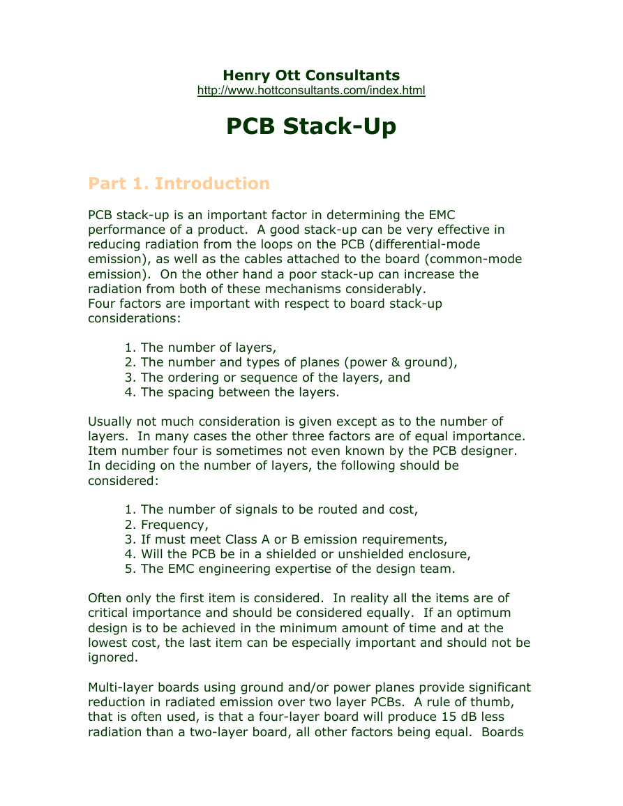
The most common four-layer board configuration is shown in Fig. 1
(power and ground planes may be reversed). It consists of four
uniformly spaced layers with internal power and ground planes. The two
external trace layers usually have orthogonal trace routing directions.
_____________ Sig.
_____________ Ground Figure 1
_____________ Power
_____________ Sig.
Although this configuration is significantly better than a two-layer
board, it has a few, less that ideal characteristics. With respect to the
list of objectives in Part 1, this stack-up only satisfies objective (1). If
the layers are equally spaced, there is a large separation between the
signal layer and the current return plane. There is also a large
separation between the power and ground planes. With a four-layer
board we cannot correct both of these deficiencies at the same time;
therefore, we must decide which is most important to us. As mentioned
previously, with normal PCB construction techniques there is not
sufficient inter-plane capacitance between the adjacent power and
ground planes to provide adequate decoupling. The decoupling,
therefore, will have to be taken care of by other means and we should
opt for tight coupling between the signal and the current return plane.
�
The advantages of tight coupling between the signal (trace) layers and
the current return planes will more than outweigh the disadvantage
caused by the slight loss in interplane capacitance.
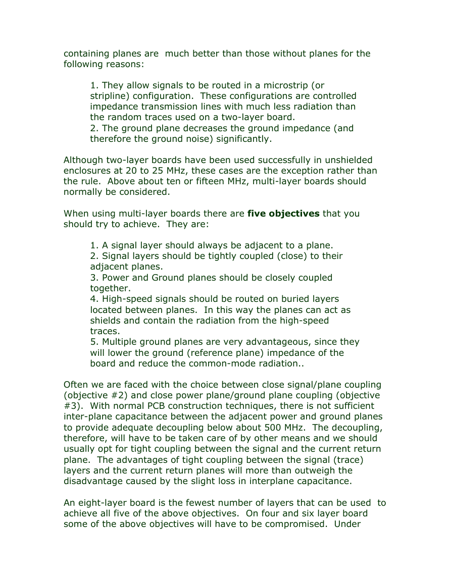
Therefore, the simplest way to improve the EMC performance of a four-
layer board is to space the signal layers as close to the planes as
possible (<0.010"), and use a large core (>0.040") between the power
and ground planes as shown in Fig. 2. This has three advantages and
few disadvantages. The signal loop areas are smaller and therefore
produce less differential mode radiation. For the case of 0.005" spacing
(trace layer to plane layer), this can amount to 10 dB or more
reduction in the trace loop radiation compared a stack-up with equally
spaced layers. Secondly, the tight coupling between the signal trace
and the ground plane reduces the plane impedance (inductance) hence
reducing the common-mode radiation from the cables connected to the
board. Thirdly, the close trace to plane coupling will decrease the
crosstalk between traces. For a fixed trace to trace spacing the
crosstalk is proportional to the square of the trace height. This is one of
the simplest, least costly, and most overlooked method of reducing
radiation on a four-layer PCB. With this configuration we have satisfied
both objectives (1) and (2).
_____________ Sig.
_____________ Ground
Figure 2
_____________ Power
_____________ Sig.
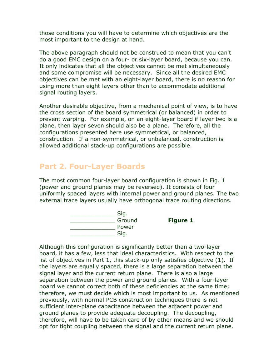
What other possibilities are there for a four-layer board stack-up? Well,
we could become a little non-conventional and reverse the signal
layers and the plane layers in Fig. 2, producing the stack-up shown in
Fig 3a.
_____________ Ground.
_____________ Sig.
Figure 3a
_____________ Sig.
_____________ Power
The major advantage of this stack-up is that the planes on the outer
layers provide shielding to the signal traces on the inner layers. The
disadvantages are that the ground plane may be cut-up considerably
with component mounting pads on a high density PCB. This can be
alleviated somewhat, by reversing the planes and placing the power
plane on the component side, and the ground plane on the other side of
the board. Secondly, some people don't like to have an exposed power
�
plane and thirdly, the buried signal layers make board rework difficult if
not impossible. This stack-up satisfies objectives (1), (2), and partially
satisfies objective (4).
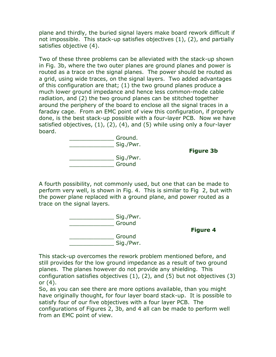
Two of these three problems can be alleviated with the stack-up shown
in Fig. 3b, where the two outer planes are ground planes and power is
routed as a trace on the signal planes. The power should be routed as
a grid, using wide traces, on the signal layers. Two added advantages
of this configuration are that; (1) the two ground planes produce a
much lower ground impedance and hence less common-mode cable
radiation, and (2) the two ground planes can be stitched together
around the periphery of the board to enclose all the signal traces in a
faraday cage. From an EMC point of view this configuration, if properly
done, is the best stack-up possible with a four-layer PCB. Now we have
satisfied objectives, (1), (2), (4), and (5) while using only a four-layer
board.
_____________ Ground.
_____________ Sig./Pwr.
Figure 3b
_____________ Sig./Pwr.
_____________ Ground
A fourth possibility, not commonly used, but one that can be made to
perform very well, is shown in Fig. 4. This is similar to Fig 2, but with
the power plane replaced with a ground plane, and power routed as a
trace on the signal layers.
_____________ Sig./Pwr.
_____________ Ground
Figure 4
_____________ Ground
_____________ Sig./Pwr.
This stack-up overcomes the rework problem mentioned before, and
still provides for the low ground impedance as a result of two ground
planes. The planes however do not provide any shielding. This
configuration satisfies objectives (1), (2), and (5) but not objectives (3)
or (4).
So, as you can see there are more options available, than you might
have originally thought, for four layer board stack-up. It is possible to
satisfy four of our five objectives with a four layer PCB. The
configurations of Figures 2, 3b, and 4 all can be made to perform well
from an EMC point of view.
�
Part 3. Six-Layer Boards
Most six-layer boards consist of four signal routing layers and two
planes. From an EMC perspective a six-layer board is usually preferred
over a four-layer board.
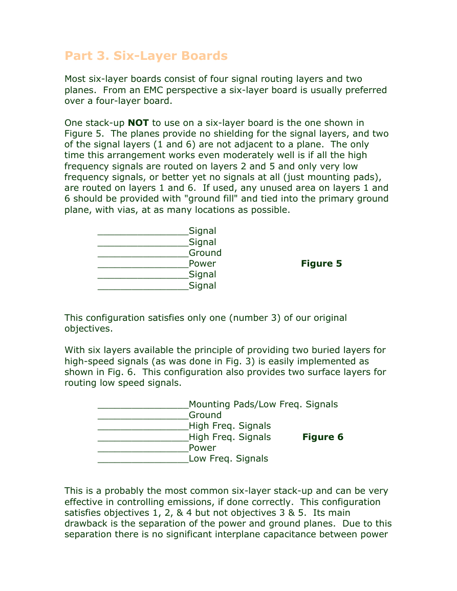
One stack-up NOT to use on a six-layer board is the one shown in
Figure 5. The planes provide no shielding for the signal layers, and two
of the signal layers (1 and 6) are not adjacent to a plane. The only
time this arrangement works even moderately well is if all the high
frequency signals are routed on layers 2 and 5 and only very low
frequency signals, or better yet no signals at all (just mounting pads),
are routed on layers 1 and 6. If used, any unused area on layers 1 and
6 should be provided with "ground fill" and tied into the primary ground
plane, with vias, at as many locations as possible.
________________Signal
________________Signal
________________Ground
________________Power Figure 5
________________Signal
________________Signal
This configuration satisfies only one (number 3) of our original
objectives.
With six layers available the principle of providing two buried layers for
high-speed signals (as was done in Fig. 3) is easily implemented as
shown in Fig. 6. This configuration also provides two surface layers for
routing low speed signals.
________________Mounting Pads/Low Freq. Signals
________________Ground
________________High Freq. Signals
________________High Freq. Signals Figure 6
________________Power
________________Low Freq. Signals
This is a probably the most common six-layer stack-up and can be very
effective in controlling emissions, if done correctly. This configuration
satisfies objectives 1, 2, & 4 but not objectives 3 & 5. Its main
drawback is the separation of the power and ground planes. Due to this
separation there is no significant interplane capacitance between power
�
and ground. Therefore, the decoupling must be designed very carefully
to account for this fact. For more information on decoupling, see
our Tech Tip on Decoupling.
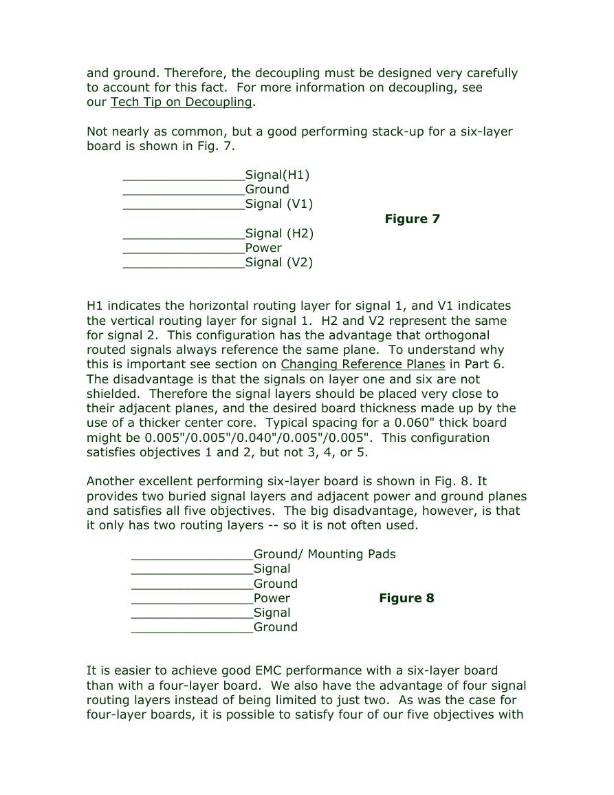
Not nearly as common, but a good performing stack-up for a six-layer
board is shown in Fig. 7.
________________Signal(H1)
________________Ground
________________Signal (V1)
Figure 7
________________Signal (H2)
________________Power
________________Signal (V2)
H1 indicates the horizontal routing layer for signal 1, and V1 indicates
the vertical routing layer for signal 1. H2 and V2 represent the same
for signal 2. This configuration has the advantage that orthogonal
routed signals always reference the same plane. To understand why
this is important see section on Changing Reference Planes in Part 6.
The disadvantage is that the signals on layer one and six are not
shielded. Therefore the signal layers should be placed very close to
their adjacent planes, and the desired board thickness made up by the
use of a thicker center core. Typical spacing for a 0.060" thick board
might be 0.005"/0.005"/0.040"/0.005"/0.005". This configuration
satisfies objectives 1 and 2, but not 3, 4, or 5.
Another excellent performing six-layer board is shown in Fig. 8. It
provides two buried signal layers and adjacent power and ground planes
and satisfies all five objectives. The big disadvantage, however, is that
it only has two routing layers -- so it is not often used.
________________Ground/ Mounting Pads
________________Signal
________________Ground
________________Power Figure 8
________________Signal
________________Ground
It is easier to achieve good EMC performance with a six-layer board
than with a four-layer board. We also have the advantage of four signal
routing layers instead of being limited to just two. As was the case for
four-layer boards, it is possible to satisfy four of our five objectives with
�
a six-layer PCB. All five objectives can be satisfied if we limit ourselves
to only two signal routing layers. The configurations of Figures 6, 7,
and 8 all can all be made to perform very well from an EMC point of
view.
Part 4. Eight-Layer Boards
An eight-layer board can be used to add two more routing layers or to
improve EMC performance by adding two more planes. Although we
see examples of both cases, I would say that the majority of eight layer
board stack-ups are used to improve EMC performance rather than add
additional routing layers. The percentage increase in cost of an eight-
layer board over a six-layer board is less than the percentage increase
in going from four to six layers, hence making it easier to justify the
cost increase for improved EMC performance. Therefore, most eight-
layer boards (and all the ones that we will concentrate on here) consist
of four wiring layers and four planes.
An eight-layer board provides us, for the first time, the opportunity to
easily satisfy all of the five originally stated objectives. Although there
are many stack-ups possible, we will only discuss a few of them that
have proven themselves by providing excellent EMC performance. As
stated above, eight layers is usually used to improve the EMC
performance of the board, not to increase the number of routing layers.
An eight-layer board with six routing layers is definitely not
recommended, no matter how you decide to stack-up the layers. If you
need six routing layers you should be using a ten-layer board.
Therefore, an eight-layer board can be thought of as a six-layer board
with optimum EMC performance.
The basic stack-up of an eight-layer board with excellent EMC
performance is shown in Fig 9.
________________Mounting Pads/Low Freq. Signals
________________Pwr.
________________Gnd.
________________High Freq. Signals
________________High Freq. Signals Figure 9
________________Gnd.
________________Pwr.
________________Low Freq. Signals/Test Pads
This configuration satisfies all the objectives listed in Part 1. All signal
�


 2023年江西萍乡中考道德与法治真题及答案.doc
 2012年重庆南川中考生物真题及答案.doc
 2013年江西师范大学地理学综合及文艺理论基础考研真题.doc
 2020年四川甘孜小升初语文真题及答案I卷.doc
 2020年注册岩土工程师专业基础考试真题及答案.doc
 2023-2024学年福建省厦门市九年级上学期数学月考试题及答案.doc
 2021-2022学年辽宁省沈阳市大东区九年级上学期语文期末试题及答案.doc
 2022-2023学年北京东城区初三第一学期物理期末试卷及答案.doc
 2018上半年江西教师资格初中地理学科知识与教学能力真题及答案.doc
 2012年河北国家公务员申论考试真题及答案-省级.doc
 2020-2021学年江苏省扬州市江都区邵樊片九年级上学期数学第一次质量检测试题及答案.doc
 2022下半年黑龙江教师资格证中学综合素质真题及答案.doc