Published on Online Documentation for Altium Products (https://www.altium.com/documentation)
主页 >
Using Altium Documentation
Modified by Jun Chu on Apr 26, 2018
Welcome to the world of electronic product development in Altium's world-class electronic
design software. This tutorial will help you get started by taking you through the entire
process of designing a simple PCB - from idea to outputs files. If you are new to Altium
software then it is worth reading the Exploring Altium Designer page to learn more about the
interface, information on how to use panels, and an overview of managing design documents.
To learn more about a command, dialog, object or panel, press F1 when the cursor is
over that item.
The Design
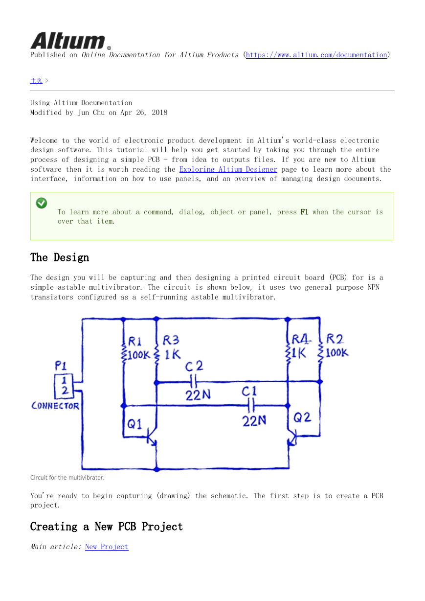
The design you will be capturing and then designing a printed circuit board (PCB) for is a
simple astable multivibrator. The circuit is shown below, it uses two general purpose NPN
transistors configured as a self-running astable multivibrator.
Circuit for the multivibrator.
You're ready to begin capturing (drawing) the schematic. The first step is to create a PCB
project.
Creating a New PCB Project
Main article: New Project
�
In Altium's software, a PCB project is the set of design documents (files) required to
specify and manufacture a printed circuit board. The project file, for example
Multivibrator.PrjPCB, is an ASCII file that lists which documents are in the project, as
well as other project-level settings, such as the required electrical rule checks, project
preferences, and project outputs, such as print and CAM settings.
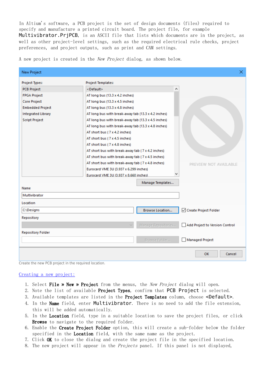
A new project is created in the New Project dialog, as shown below.
Create the new PCB project in the required location.
Creating a new project:
1.
2.
3.
4.
5.
6.
7.
8.
Select File » New » Project from the menus, the New Project dialog will open.
Note the list of available Project Types, confirm that PCB Project is selected.
Available templates are listed in the Project Templates column, choose .
In the Name field, enter Multivibrator. There is no need to add the file extension,
this will be added automatically.
In the Location field, type in a suitable location to save the project files, or click
Browse to navigate to the required folder.
Enable the Create Project Folder option, this will create a sub-folder below the folder
specified in the Location field, with the same name as the project.
Click OK to close the dialog and create the project file in the specified location.
The new project will appear in the Projects panel. If this panel is not displayed,
�
click the
Files from the menu that appears.
button at the bottom right of the main design window, and select
Enabling the Add Project to Version Control option will result in the project's
source files being stored in an available SVN repository (click Managed
Repositories), and check out the working copies into the folder specified in the
Location field. To learn more about version control support, refer to the Version
Control and Design Repositories article.
If the Managed Project option is enabled, the source files are stored stored in an
available SVN repository and the project outputs are stored in an available Altium
Vault. To learn more about Managed Projects, refer to the article, The Managed
Project and Releasing the Design.
These features will not be used for this tutorial.
�
Adding a Schematic to the Project
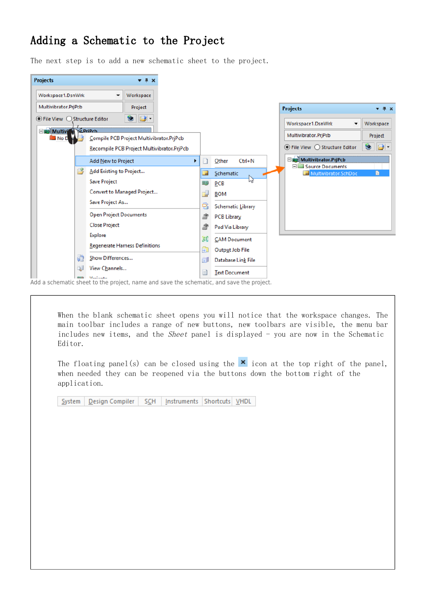
The next step is to add a new schematic sheet to the project.
Add a schematic sheet to the project, name and save the schematic, and save the project.
When the blank schematic sheet opens you will notice that the workspace changes. The
main toolbar includes a range of new buttons, new toolbars are visible, the menu bar
includes new items, and the Sheet panel is displayed - you are now in the Schematic
Editor.
The floating panel(s) can be closed using the
when needed they can be reopened via the buttons down the bottom right of the
application.
icon at the top right of the panel,
�
Adding a schematic:
1.
2.
3.
Right-click on the project filename in the Projects panel, and select Add New to
Project » Schematic. A blank schematic sheet named Sheet1.SchDoc will open in the
design window and an icon for this schematic will appear linked to the project in the
Projects panel, under the Source Documents folder icon.
To save the new schematic sheet, select File » Save As. The Save As dialog will open,
ready to save the schematic in the same location as the project file. Type the name
Multivibrator in the File Name field and click Save. Note that files stored in the
same folder as the project file itself (or in a child/grandchild folder) are linked to
the project using relative referencing, whereas files stored in a different location
are linked using absolute referencing.
Since you have added a schematic to the project, the project file has changed too.
Right-click on the project filename in the Projects panel, and select Save Project to
save the project.
Setting the Document Options
Main article: Document Options
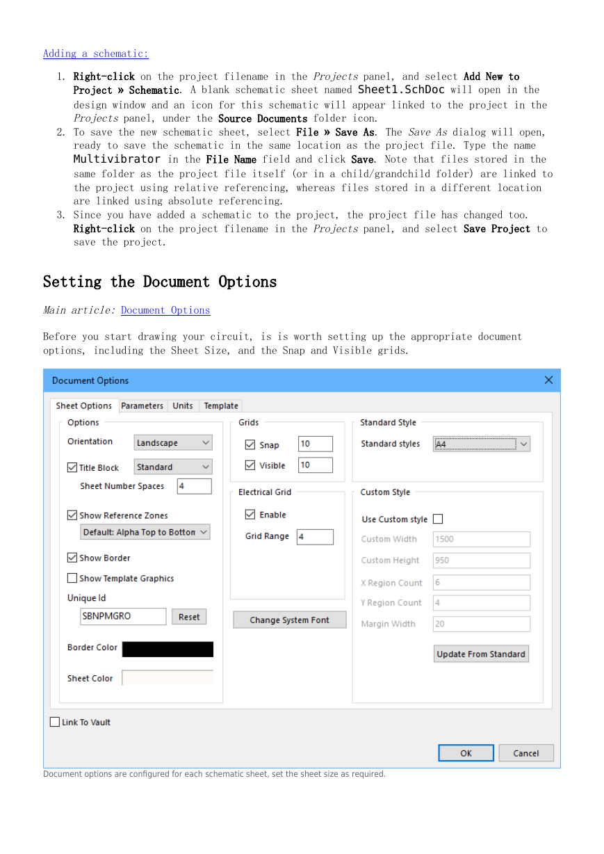
Before you start drawing your circuit, is is worth setting up the appropriate document
options, including the Sheet Size, and the Snap and Visible grids.
Document options are configured for each schematic sheet, set the sheet size as required.
�
As well as the technique described in the collapsible section below, the Document
Options dialog can be opened by double-clicking in the sheet border.
Environment options, such as the cursor type, selection color and auto pan behavior
are configured in the Preferences dialog (File » System Preferences).
�
Configuring the Document Options:
1.
2.
3.
4.
5.
6.
From the menus, choose Design » Document Options to open the Document Options dialog.
For this tutorial, the only change we need to make here is to set the sheet size to A4,
this is done in the Standard Styles field of the Sheet Options tab of the dialog.
Confirm that both the Snap and Visible Grids are set to 10.
Click OK to close the dialog and update the sheet size.
To make the document fill the viewing area, select View » Fit Document (shortcut: V,
D).
Save the schematic by selecting File » Save (shortcut: F, S).
Components and Libraries in Altium Designer
Related article: More about Components and Libraries
This section of the tutorial will explain the two different approaches to working
with components (from libraries, or from the Vault). In the following section, you
will locate and place the components you need, from the Vault.
The real-world component that gets mounted on the board is represented as a schematic symbol
during design capture, and as a PCB footprint for board design. Altium Designer components
can be:
created in and placed from local libraries, or
placed directly from the Altium Content Vault, a globally accessible component storage
system that contains thousands of components, each with a symbol, footprint, component
parameters and links to suppliers.
The following component storage options can be used in Altium Designer:
Library Type
Schematic
Library
PCB Library
Library Package
/ Integrated
Library
Altium Content
Vault
Function
Schematic component symbols are created in schematic libraries (*.SchLib), which are stored
locally. Each symbol can become a component by adding links to a PCB footprint, then adding
component parameters to detail the component's specifications.
PCB footprints (models) are stored in PCB libraries (*.PcbLib), which are stored locally.
The footprint includes the electrical elements, such as the pads, as well as the mechanical
elements, such as the component overlay, dimensions, glue dots, and so on. It can also include
a 3D definition, created by placing 3D Body objects, or by importing a STEP model.
As well as working directly from the schematic and PCB libraries, you can also compile the
component elements into an integrated library (*.IntLib, stored locally). Doing this results
in a single, portable library which holds all the models and symbols. An integrated library is
compiled from a Library package (*.LibPkg), which is essentially a special-purpose project
file, with the source schematic (*.SchLib) and PCB libraries (*.PcbLib) added to it as
source documents. As part of the compilation process, you can also check for potential
problems, such as missing models and mismatches between schematic pins and PCB pads.
The Content Vault is much more than a library. Components are stored in the cloud, accessible
from anywhere that has internet access. Content Vault components include: symbol,
footprint(s), component parameters, and links to suppliers. They are organized into folders -
by manufacturer, or by package type for generics.
Accessing Components
Components are accessed through the:
�
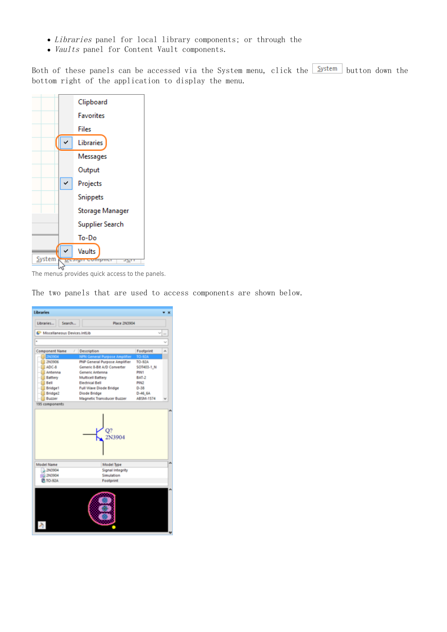
Libraries panel for local library components; or through the
Vaults panel for Content Vault components.
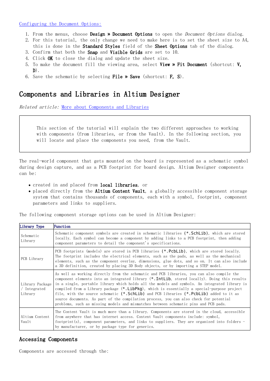
Both of these panels can be accessed via the System menu, click the
bottom right of the application to display the menu.
button down the
The menus provides quick access to the panels.
The two panels that are used to access components are shown below.
�



 2023年江西萍乡中考道德与法治真题及答案.doc
 2012年重庆南川中考生物真题及答案.doc
 2013年江西师范大学地理学综合及文艺理论基础考研真题.doc
 2020年四川甘孜小升初语文真题及答案I卷.doc
 2020年注册岩土工程师专业基础考试真题及答案.doc
 2023-2024学年福建省厦门市九年级上学期数学月考试题及答案.doc
 2021-2022学年辽宁省沈阳市大东区九年级上学期语文期末试题及答案.doc
 2022-2023学年北京东城区初三第一学期物理期末试卷及答案.doc
 2018上半年江西教师资格初中地理学科知识与教学能力真题及答案.doc
 2012年河北国家公务员申论考试真题及答案-省级.doc
 2020-2021学年江苏省扬州市江都区邵樊片九年级上学期数学第一次质量检测试题及答案.doc
 2022下半年黑龙江教师资格证中学综合素质真题及答案.doc