应用报告
ZHCA059–2007 年 12 月
USB 2.0 板载设计及布线指南
DSP 应用
本文档探讨了通用串行总线(USB)系统原理图设计的若干指导方针。
摘要
1 背景
2 USB 物理层(PHY)布线指南
3 静电放电(ESD)
4 参考文献
目录
图表目录
1 推荐的电容及铁氧体磁珠阵列,以实现电磁干扰的最小化
2 四层板堆叠
3 USB 连接器
4 3W 间隔规则
5 至 USB 物理层的电源及时钟连接
6 USB 物理层连接器及缆线连接器
7 避免跨层边界走线
8 避免层交叠
9 避免损坏镜像层
1
2
8
10
2
3
4
4
5
6
7
7
8
1
背景
在 USB 设计中,时钟频率提供了主要的信号源。USB 差分 DP/DM 对可工作于 480Mbps的高速模式,系
统时钟可工作于 12 MHz、48 MHz 及 60 MHz。由于 USB 电缆扮演了单极天线的角色,因此必须小心设计
以防止 RF 电流耦合至缆线上。
设计 USB 板载时,最关注的信号有:
•
•
•
•
器件接口信号:时钟及其他信号/数据,通过走线在器件与 PCB 之间传输。
缆线输入/输出供电:USB 连接器插槽的引脚 1(VBUS)可能被严重滤波,仅可通过低于 100 KHz的低频信
号。USB 插槽的引脚 4(模拟地)必须能够返还(return)数据传输期间的电流,且必须进行基本的滤波。
通过缆线、DP 及 DM 输出出的差分双铰线对信号:依据数据传输率的不同,这些器件的终端引脚上可
给出带 240MHz (高速)、6MHz (全速)、750kHz (低速)基频的信号。
外部晶振电路(器件终端引脚 XI 及 X0):12MHz、19.2MHz、24MHz、48MHz 基频。如果使用外接
晶体作为参考时钟,强烈推荐采用 24MHz 及 更高基频的晶振。
ZHCA059–2007 年 12 月
提交文档反馈
USB 2.0 板载设计及布线指南
�
�
USB 物理层布线指南
2
USB 物理层布线指南
http://www.ti.com.cn
www.ti.com
2.1 General Routing and Placement
USB PHY Layout Guide
2
2.1
下列章节将详细讲述 USB 物理层布线的特定指导方针。
USB PHY Layout Guide
一般走线(Routing)及安置(Placement)
The following sections describe in detail the specific guidelines for USB PHY Layout.
在对 USB 物理层(PHY)进行新的设计布线时,请遵循下列的走线及安置指导方针。此类指导方针有助于最
小化 4 层或更多层级评估板(EVM)设计相关的信号品质及电磁干扰(EMI)问题。
Use the following routing and placement guidelines when laying out a new design for the USB physical
layer (PHY). These guidelines help minimize signal quality and electromagnetic interference (EMI)
•
problems on a four-or-more layer evaluation module (EVM).
•
• Place the USB PHY and major components on the un-routed board first. For more details, see
•
•
• Route the high-speed clock and high-speed USB differential signals with minimum trace lengths.
• Route the high-speed USB signals on the plane closest to the ground plane, whenever possible.
•
• Route the high-speed USB signals using a minimum of vias and corners. This reduces signal
•
• When it becomes necessary to turn 90°, use two 45° turns or an arc instead of making a single 90°
首先将 USB 物理层及主要元件放置于未走线(un-routed)板载上。如需更多详细信息,敬请参见 2.2.3 节。
以最小化的迹线(trace)长度布置高速时钟及高速 USB 差分信号的走线。
在有可能的时候,将板上的高速 USB 信号线布置于尽可能靠近接地平面的位置。
Section 2.2.3.
以最少的穿孔(via)及弯折(corner)实现高速 USB 信号的走线,以减少信号的反射(reflection)及阻抗改变。
当不得不采取 90°弯折走线时,以两个 45°弯折或圆弧形的走线替代单个 90°的弯折,以通过最小化
阻抗的非连续(discontinuity)实现信号迹线上反射的降低。
reflections and impedance changes.
晶振、振荡器、时钟信号发生器、开关稳压器、安装穿孔(mounting hole)、磁器件或 IC 的下方或附近不
进行 USB 迹线的走线。
turn. This reduces reflections on the signal traces by minimizing impedance discontinuities.
避免因高速 USB 信号的残桩(stub)而引起信号的反射。如果残桩无法避免,则残桩应短于200 mils。
regulators, mounting holes, magnetic devices or IC’s that use or duplicate clock signals.
通过连续的层(plane,VCC 或 GND)实现非中断性的高速 USB 信号走线,以避免层分割(plane split)中常
遇到的交叉分隔覆铜(anti-etch)问题。
unavoidable, then the stub should be less than 200 mils.
•
• Do not route USB traces under or near crystals, oscillators, clock signal generators, switching
•
• Avoid stubs on the high-speed USB signals because they cause signal reflections. If a stub is
2.2
• Route all high-speed USB signal traces over continuous planes (VCC or GND), with no interruptions.
针对 USB 物理层布线的特点指导方针
Avoid crossing over anti-etch, commonly found with plane splits.
下列章节将详细讲述 USB 物理层布线的特定指导方针。
2.2 Specific Guidelines for USB PHY Layout
2.2.1
模拟、锁相环及数字电源滤波
The following sections describe in detail the specific guidelines for USB PHY Layout.
2.2.1
为了最小化电磁干扰辐射,可在芯片的模拟、锁相环(PLL)及数字部分的电源终端引脚上添加带铁氧体
Analog, PLL, and Digital Power Supply Filtering
磁珠(ferrite bead)的去耦合电容。该去耦合阵列应布置于尽可能的靠近芯片的位置,以实现线路自感及
To minimize EMI emissions, add decoupling capacitors with a ferrite bead at power supply terminals for
the analog, phase-locked loop (PLL), and digital portions of the chip. Place this array as close to the chip
对系统的噪声影响的最小化。图1所示为模拟及数字电源的示例。当碰上多个电源引脚实现同一功能的
as possible to minimize the inductance of the line and noise contributions to the system. An analog and
情况,可将其汇聚至单个板上的低阻抗端点,而后添加去耦合电容及铁氧体磁珠。此类电容及铁氧体磁
digital supply example is shown in Figure 1. In case of multiple power supply pins with the same function,
珠的阵列有助于改善 EMI 及抗抖动(jitter)性能,因此在对配置进行修改之前,应当同时把 EMI 及抖动
tie them up to a single low-impedance point in the board and then add the decoupling capacitors, in
addition to the ferrite bead. This array of caps and ferrite bead improve EMI and jitter performance. Take
纳入考虑。
both EMI and jitter into account before altering the configuration.
Analog
Power�Supply
Ferrite�Bead
Digital
Power�Supply
Ferrite�Bead
0.1�µF
0.01�µF
0.001�µF
10�µF
SoC�Board
0.1�µF
0.01�µF
0.001�µF
10�µF
Figure 1. Suggested Array Capacitors and a Ferrite Bead to Minimize EMI
图1. 推荐的电容及铁氧体磁珠阵列,以实现电磁干扰的最小化
� USB 2.0 板载设计及布线指南
ZHCA059–2007 年 12 月
提交文档反馈
�
http://www.ti.com.cn
USB 物理层布线指南
考虑下列建议以实现适当的静电放电/电磁干扰性能:
www.ti.com
•
•
USB PHY Layout Guide
在每条缆线供电 VBUS 线路上采用单个 0.01 mF 电容连接至 USB 连接器引脚附近的外壳接地点
(chassis GND)。
在每条缆线接地线上采用单个 0.01 mF 电容连接至与 USB 连接器引脚附近的 chassis GND。
如果采用了电压稳压器,则同时在输入及输出端放置 0.01 mF 的电容。该措施可增强对静电放电的
免疫能力并降低电磁干扰。对于其他的需求,敬请参见特定器件的数据表。
Consider the recommendations listed below to achieve proper ESD/EMI performance:
• Use a 0.01 µF cap on each cable power VBUS line to chassis GND close to the USB connector pin.
• Use a 0.01 µF cap on each cable ground line to chassis GND next to the USB connector pin.
•
•
If voltage regulators are used, place a 0.01 µF cap on both input and output. This is to increase the
immunity to ESD and reduce EMI. For other requirements, see the device-specific datasheet.
2.2.2
2.2.2
模拟、数字及锁相环的剖分(Partitioning)
Analog, Digital, and PLL Partitioning
如果采用了分离的电源层(power plane),则电源层之间必须通过低阻抗的桥接或铁氧体磁珠汇聚至一
If separate power planes are used, they must be tied together at one point through a low-impedance
bridge or preferably through a ferrite bead. Care must be taken to capacitively decouple each power rail
点。同时必须小心谨慎的处理每条接近器件的电源导轨的电容性去耦合。模拟地、数字地及锁相环接地
close to the device. The analog ground, digital ground, and PLL ground must be tied together to the
则必须汇聚至低阻抗的电路板接地层。
low-impedance circuit board ground plane.
2.2.3
2.2.3
板层堆叠
Board Stackup
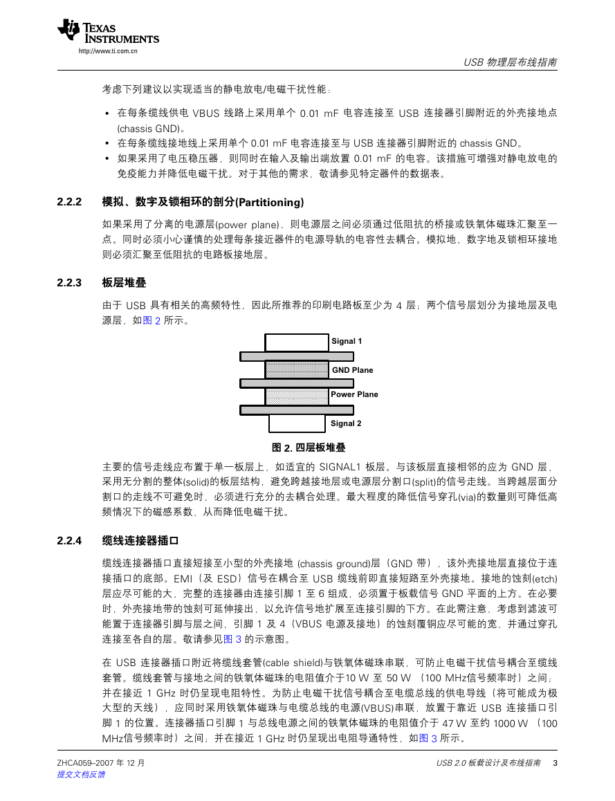
由于 USB 具有相关的高频特性,因此所推荐的印刷电路板至少为 4 层;两个信号层划分为接地层及电
Because of the high frequencies associated with the USB, a printed circuit board with at least four layers
is recommended; two signal layers separated by a ground and power layer as shown in Figure 2.
源层,如图 2 所示。
Signal�1
GND�Plane
Power�Plane
Signal�2
2.2.4
2.2.4
Figure 2. Four-Layer Board Stack-Up
图 2. 四层板堆叠
The majority of signal traces should run on a single layer, preferably SIGNAL1. Immediately next to this
layer should be the GND plane, which is solid with no cuts. Avoid running signal traces across a split in
the ground or power plane. When running across split planes is unavoidable, sufficient decoupling must
be used. Minimizing the number of signal vias reduces EMI by reducing inductance at high frequencies.
主要的信号走线应布置于单一板层上,如适宜的 SIGNAL1 板层。与该板层直接相邻的应为 GND 层,
采用无分割的整体(solid)的板层结构,避免跨越接地层或电源层分割口(split)的信号走线。当跨越层面分
割口的走线不可避免时,必须进行充分的去耦合处理。最大程度的降低信号穿孔(via)的数量则可降低高
频情况下的磁感系数,从而降低电磁干扰。
Cable Connector Socket
缆线连接器插口
Short the cable connector sockets directly to a small chassis ground plane (GND strap) that exists
immediately underneath the connector sockets. This shorts EMI (and ESD) directly to the chassis ground
缆线连接器插口直接短接至小型的外壳接地 (chassis ground)层(GND 带),该外壳接地层直接位于连
before it gets onto the USB cable. This etch plane should be as large as possible, but all the conductors
接插口的底部。EMI(及 ESD)信号在耦合至 USB 缆线前即直接短路至外壳接地。接地的蚀刻(etch)
coming off connector pins 1 through 6 must have the board signal GND plane run under. If needed, scoop
层应尽可能的大,完整的连接器由连接引脚 1 至 6 组成,必须置于板载信号 GND 平面的上方。在必要
out the chassis GND strap etch to allow for the signal ground to extend under the connector pins. Note
that the etches coming from pins 1 and 4 (VBUS power and GND) should be wide and via-ed to their
时,外壳接地带的蚀刻可延伸接出,以允许信号地扩展至连接引脚的下方。在此需注意,考虑到滤波可
respective planes as soon as possible, respecting the filtering that may be in place between the connector
能置于连接器引脚与层之间,引脚 1 及 4(VBUS 电源及接地)的蚀刻覆铜应尽可能的宽,并通过穿孔
pin and the plane. See Figure 3 for a schematic example.
连接至各自的层。敬请参见图 3 的示意图。
Place a ferrite in series with the cable shield pins near the USB connector socket to keep EMI from getting
onto the cable shield. The ferrite bead between the cable shield and ground may be valued between 10 Ω
在 USB 连接器插口附近将缆线套管(cable shield)与铁氧体磁珠串联,可防止电磁干扰信号耦合至缆线
and 50 Ω at 100 MHz; it should be resistive to approximately 1 GHz. To keep EMI from getting onto the
套管。缆线套管与接地之间的铁氧体磁珠的电阻值介于10 W 至 50 W (100 MHz信号频率时)之间;
cable bus power wire (a very large antenna) a ferrite may be placed in series with cable bus power,
VBUS, near the USB connector pin 1. The ferrite bead between connector pin 1 and bus power may be
并在接近 1 GHz 时仍呈现电阻特性。为防止电磁干扰信号耦合至电缆总线的供电导线(将可能成为极
valued between 47 Ω and approximately 1000 Ω at 100 MHz. It should continue being resistive out to
大型的天线),应同时采用铁氧体磁珠与电缆总线的电源(VBUS)串联,放置于靠近 USB 连接插口引
approximately 1 GHz, as shown in Figure 3.
脚 1 的位置。连接器插口引脚 1 与总线电源之间的铁氧体磁珠的电阻值介于 47 W 至约 1000 W (100
MHz信号频率时)之间;并在接近 1 GHz 时仍呈现出电阻导通特性,如图 3 所示。
ZHCA059–2007 年 12 月
提交文档反馈
USB 2.0 板载设计及布线指南
�
�
USB PHY Layout Guide
USB 物理层布线指南
USB PHY Layout Guide
VBUS
VBUS
Ferrite�Bead
Ferrite�Bead
U2
U2
U1
U1
Ferrite�Bead
Ferrite�Bead
Figure 3. USB Connector
图3. USB 连接器
www.ti.com
http://www.ti.com.cn
www.ti.com
5
4
5
3
4
2
3
1
2
6
1
6
SHIELD_GND
GND
SHIELD_GND
DP
GND
DM
DP
+5�V
DM
SHIELD_GND
+5�V
USB�Socket
SHIELD_GND
USB�Socket
Figure 3. USB Connector
2.2.5
2.2.5
2.2.5
时钟走线
Clock Routings
为满足系统器件间时钟辐射的需求,须安置约 10 至 130 W 的电阻与时钟信号串联。采用试错法(trial
To address the system clock emissions between devices, place a ~10 to 130 Ω resistor in series with the
Clock Routings
clock signal. Use a trial and error method of looking at the shape of the clock waveform on a high-speed
and error),通过高速的示波器查看时钟波形并调节电阻值,以实现最小化的波形失真。此电阻值应尽
oscilloscope and of tuning the value of the resistance to minimize waveform distortion. The value on this
To address the system clock emissions between devices, place a ~10 to 130 Ω resistor in series with the
可能的小以实现所期望的效果。电阻应放置于靠近时钟信号生成器件的位置。如果采用了外部晶振,则
resistor should be as small as possible to get the desired effect. Place the resistor close to the device
clock signal. Use a trial and error method of looking at the shape of the clock waveform on a high-speed
generating the clock signal. If an external crystal is used, follow the guidelines detailed in the Selection
应遵循 Selection and Specification of Crystals for Texas Instruments USB 2.0 Devices (SLLA122) 一文
oscilloscope and of tuning the value of the resistance to minimize waveform distortion. The value on this
and Specification of Crystals for Texas Instruments USB 2.0 Devices (SLLA122).
resistor should be as small as possible to get the desired effect. Place the resistor close to the device
中所述的详细指导方针。
generating the clock signal. If an external crystal is used, follow the guidelines detailed in the Selection
When routing the clock traces from one device to another, try to use the 3W spacing rule. The distance
and Specification of Crystals for Texas Instruments USB 2.0 Devices (SLLA122).
当进行器件间时钟迹线的布线时,可尝试使用 3 W 间隔规则。即时钟迹线的中心至任意临近的信号迹
from the center of the clock trace to the center of any adjacent signal trace should be at least three times
the width of the clock trace. Many clocks, including slow frequency clocks, can have fast rise and fall
When routing the clock traces from one device to another, try to use the 3W spacing rule. The distance
线中心的距离应至少为 3 倍的时钟迹线宽度。许多时钟,包括低频时钟在内,其上升时间及下降时间都
times. Using the 3W rule cuts down on crosstalk between traces. In general, leave space between each of
from the center of the clock trace to the center of any adjacent signal trace should be at least three times
有可能很短。采用 3 W 规则可削减迹线间的串扰。一般来说,器件间并行的走线之间也应当保持一定
the traces running parallel between the devices. Avoid using right angles when routing traces to minimize
the width of the clock trace. Many clocks, including slow frequency clocks, can have fast rise and fall
the routing distance and impedance discontinuities. For further protection from crosstalk, run guard traces
的距离,并避免采用直角走线,以最小化走线长度及阻抗的非连续性。为更进一步的防护串扰,如果有
times. Using the 3W rule cuts down on crosstalk between traces. In general, leave space between each of
beside the clock signals (GND pin to GND pin), if possible. This lessens clock signal coupling, as shown in
the traces running parallel between the devices. Avoid using right angles when routing traces to minimize
可能,可在时钟信号线旁侧走保护迹线(guard trace,GND 引脚至 GND 引脚)。上述方法均可以减少时
Figure 4.
the routing distance and impedance discontinuities. For further protection from crosstalk, run guard traces
钟信号的耦合,如图 4 所示。
beside the clock signals (GND pin to GND pin), if possible. This lessens clock signal coupling, as shown in
Figure 4.
3W
3W
3W
3W
Trace
Trace
W
Figure 4. 3W Spacing Rule
W
Figure 4. 3W Spacing Rule
图4. 3W 间隔规则
4
� USB 2.0 板载设计及布线指南
USB 2.0 Board Design and Layout Guidelines
4
USB 2.0 Board Design and Layout Guidelines
SPRAAR7–December 2007
ZHCA059–2007 年 12 月
Submit Documentation Feedback
提交文档反馈
SPRAAR7–December 2007
Submit Documentation Feedback
�
http://www.ti.com.cn
USB 物理层布线指南
2.2.6
www.ti.com
晶振/振荡器
2.2.6
USB PHY Layout Guide
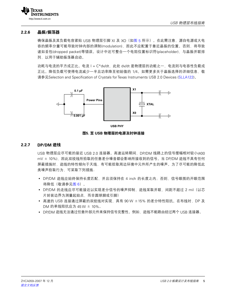
确保晶振及其负载电容紧贴 USB 物理层引脚 XI 及 XO(如图 5 所示)。在此需注意,源自电源或大电
Crystals/Oscillator
容的频率分量可能导致时钟内部的调制(modulation),因此不应配置于靠近晶振的位置。否则,将导致
Keep the crystal and its load capacitors close to the USB PHY pins, XI and XO (see Figure 5). Note that
诸如丢包(dropped packet)等错误。设计中还可整合一个电阻位置标识符(placeholder),与晶振并联排
frequencies from power sources or large capacitors can cause modulations within the clock and should
列,以用于辅助振荡器启动。
not be placed near the crystal. In these instances, errors such as dropped packets occur. A placeholder
for a resistor, in parallel with the crystal, can be incorporated in the design to assist oscillator startup.
功耗与电流的平方成正比。电流 I = C*dv/dt,此处 dv/dt 是物理层的功能之一,电流则与电容性负载成
Power is proportional to the current squared. The current is I = C*dv/dt, since dv/dt is a function of the
正比。降低负载可使得电流减少一半且功率降至初始值的 1/4。如需更多关于晶振选择的详细信息,敬
PHY, current is proportional to the capacitive load. Cutting the load to decreases the current by and the
power to 1/4 the original value. For more details on crystal selection, see the Selection and Specification
请参见Selection and Specification of Crystals for Texas Instruments USB 2.0 Devices (SLLA122)。
of Crystals for Texas Instruments USB 2.0 Devices (SLLA122).
Power�Pins
0.1�µF
0.001�µF
X1
X0
XTAL
Figure 5. Power Supply and Clock Connection to the USB PHY
图5. 至 USB 物理层的电源及时钟连接
USB�PHY
2.2.7
2.2.7
DP/DM 迹线
DP/DM Trace
USB 物理层应尽可能的接近 USB 2.0 连接器。高速运转期间,DP/DM 线路上的信号摆幅相对较小(400
mV ± 10%),因此双绞线所拾取的任意差分噪音都会影响所接收到的信号。当 DP/DM 迹线不具有任何
屏蔽措施时,迹线的特性倾向于天线,有可能拾取周边环境中元件所产生的噪声。为了尽可能的降低此
Place the USB PHY as close as possible to the USB 2.0 connector. The signal swing during high-speed
operation on the DP/DM lines is relatively small (400 mV ± 10%), so any differential noise picked up on
the twisted pair can affect the received signal. When the DP/DM traces do not have any shielding, the
traces tend to behave like an antenna and picks up noise generated by the surrounding components in
the environment. To minimize the effect of this behavior:
• DP/DM traces should always be matched lengths and must be no more than 4 inches in length;
类噪声拾取行为,可采取下列措施:
otherwise, the eye opening may be degraded (see Figure 6).
•
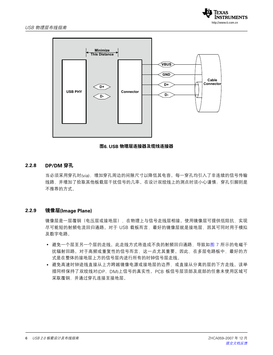
DP/DM 迹线应始终保持长度匹配,并且须保持在 4 inch 的长度之内;否则,信号眼图的开眼范围
• Route DP/DM traces close together for noise rejection on differential signals, parallel to each other and
将降低(敬请参见图 6)。
within two mils in length of each other (start the measurement at the chip package boundary, not to the
DP/DM 的走线应尽可能接近以实现差分信号的噪声抑制,迹线采取并联,间距不超过 2 mil(以芯
•
balls or pins).
片封装边界为测量起始点,而非圆球脚或引脚)
characteristic impedance of 90 Ω ±15%. In layout, the impedance of DP and DM should each be 45 Ω
高速的 USB 连接通过屏蔽的双绞线对实现,具有 90 W ±15% 的差分特性阻抗。在布线时,DP 及
•
± 10%.
DM 的单线阻抗应为 45 W ± 10%。
• DP/DM traces should not have any extra components to maintain signal integrity. For example, traces
DP/DM 迹线无法通过任意外部元件来保持信号完整性。例如,迹线不能路由经过两个 USB 连接器。
• A high-speed USB connection is made through a shielded, twisted pair cable with a differential
•
cannot be routed to two USB connectors.
ZHCA059–2007 年 12 月
提交文档反馈
SPRAAR7–December 2007
USB 2.0 板载设计及布线指南
�
USB 2.0 Board Design and Layout Guidelines
5
�
USB 物理层布线指南
USB PHY Layout Guide
http://www.ti.com.cn
www.ti.com
Minimize
This�Distance
USB�PHY
D+
D-
Connector
VBUS
GND
D+
D-
Cable
Connector
2.2.8
2.2.8
2.2.9
2.2.9
Figure 6. USB PHY Connector and Cable Connector
图6. USB 物理层连接器及缆线连接器
DP/DM Vias
DP/DM 穿孔
When a via must be used, increase the clearance size around it to minimize its capacitance. Each via
introduces discontinuities in the signal’s transmission line and increases the chance of picking up
当必须采用穿孔时(via),增加穿孔周边的间隙尺寸以降低其电容。每一穿孔均引入了非连续的信号传输
interference from the other layers of the board. Be careful when designing test points on twisted pair lines;
through-hole pins are not recommended.
线路,并增加了拾取其他板载层干扰信号的几率。在设计双绞线上的测点时须小心谨慎;穿孔引脚则是
不推荐的方式。
Image Planes
镜像层(Image Plane)
An image plane is a layer of copper (voltage plane or ground plane), physically adjacent to a signal routing
plane. Use of image planes provides a low impedance, shortest possible return path for RF currents. For a
USB board, the best image plane is the ground plane because it can be used for both analog and digital
circuits.
镜像层是一层覆铜(电压层或接地层),在物理上与信号走线层相接。使用镜像层可提供低阻抗,实现
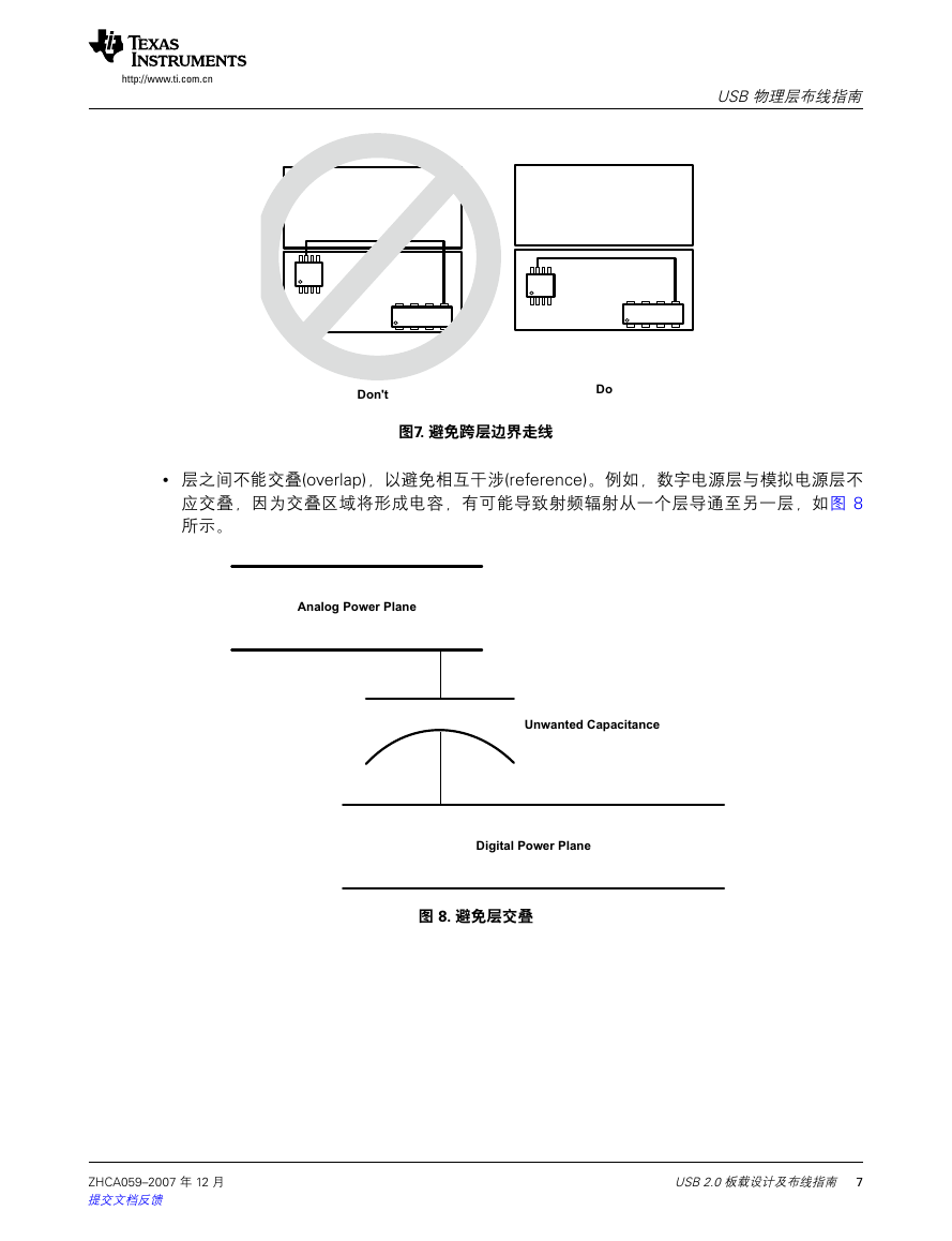
• Do not route traces so they cross from one plane to the other. This can cause a broken RF return path
尽可能短的射频电流回归通路。对于 USB 载板而言,最好的镜像层就是接地层,因其可同时用于模拟
resulting in an EMI radiating loop as shown in Figure 7. This is important for higher frequency or
repetitive signals. Therefore, on a multi-layer board, it is best to run all clock signals on the signal
及数字电路。
plane above a solid ground plane.
避免一个层至另一个层的走线。此走线方式将造成不良的射频回归通路,导致如图 7 所示的电磁干
•
immediately above or below the separated planes. This also holds true for the twisted pair signals (DP,
扰辐射回路。对于高频或重复性的信号而言,这一点尤其重要。因此,在多层电路板中,最好的方
DM). Any unused area of the top and bottom signal layers of the PCB can be filled with copper that is
connected to the ground plane through vias.
•
• Avoid crossing the image power or ground plane boundaries with high-speed clock signal traces
式是在整体的接地层上方的信号层内进行所有的时钟信号层走线。
避免高速时钟迹线直接从上方跨越镜像电源或接地层的边界,或直接从分离的层的下方走线。该举
措同样保持了双绞线对(DP、DM)上信号的真实性。PCB 板信号层顶部及底部的任意未使用区域可
采取覆铜,并通过穿孔连接至接地层。
6
� USB 2.0 板载设计及布线指南
USB 2.0 Board Design and Layout Guidelines
SPRAAR7–December 2007
ZHCA059–2007 年 12 月
Submit Documentation Feedback
提交文档反馈
�
www.ti.com
http://www.ti.com.cn
www.ti.com
USB 物理层布线指南
USB PHY Layout Guide
USB PHY Layout Guide
Don't
Do
Figure 7. Do Not Cross Plane Boundaries
图7. 避免跨层边界走线
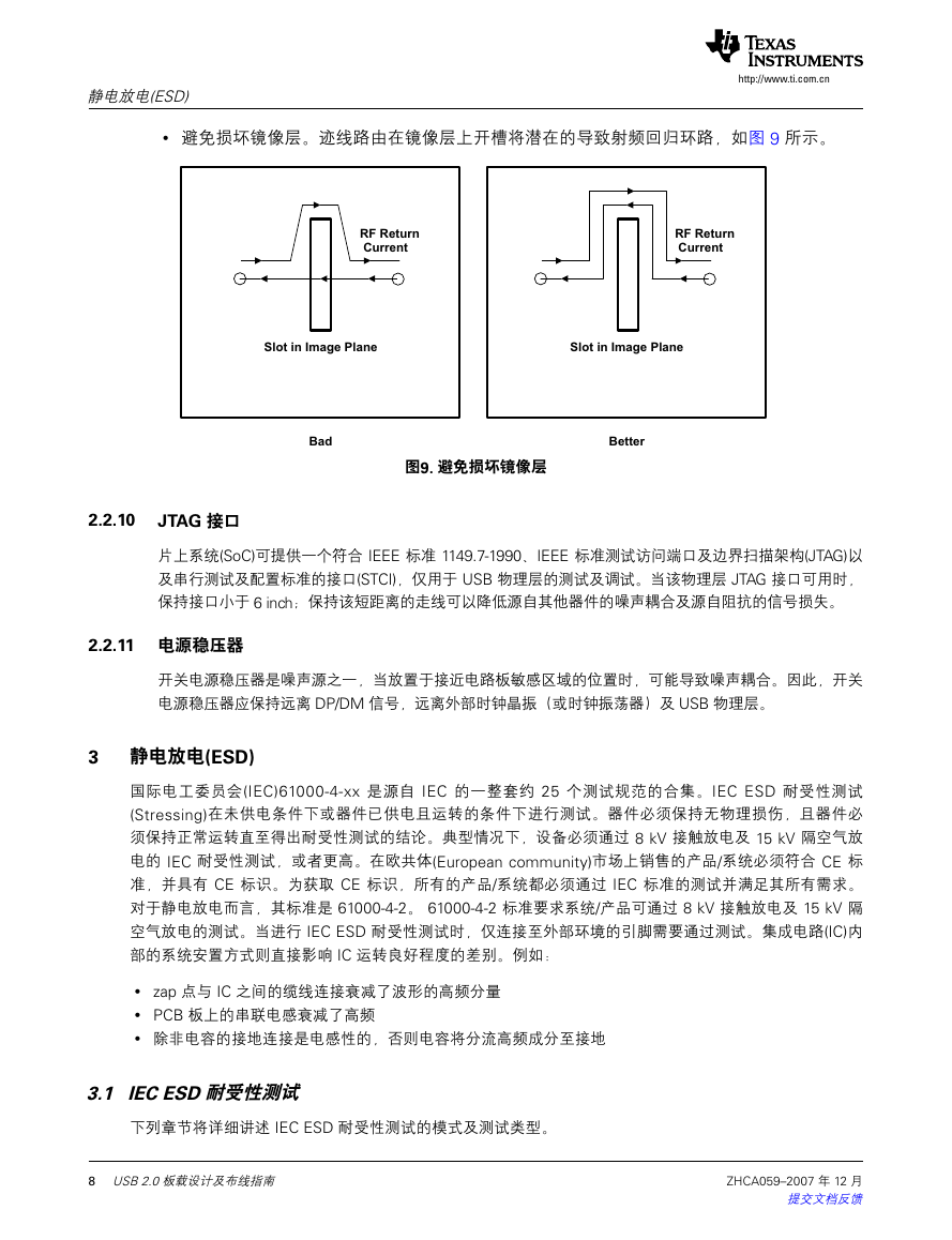
• Do not overlap planes that do not reference each other. For example, do not overlap a digital power
Don't
Do
• Do not overlap planes that do not reference each other. For example, do not overlap a digital power
plane with an analog power plane as this produces a capacitance between the overlapping areas that
层之间不能交叠(overlap),以避免相互干涉(reference)。例如,数字电源层与模拟电源层不
•
could pass RF emissions from one plane to the other, as shown in Figure 8.
应交叠,因为交叠区域将形成电容,有可能导致射频辐射从一个层导通至另一层,如图 8
plane with an analog power plane as this produces a capacitance between the overlapping areas that
所示。
could pass RF emissions from one plane to the other, as shown in Figure 8.
Figure 7. Do Not Cross Plane Boundaries
Analog�Power�Plane
Analog�Power�Plane
Unwanted�Capacitance
Unwanted�Capacitance
Digital�Power�Plane
Digital�Power�Plane
Figure 8. Do Not Overlap Planes
Figure 8. Do Not Overlap Planes
图 8. 避免层交叠
ZHCA059–2007 年 12 月
SPRAAR7–December 2007
Submit Documentation Feedback
提交文档反馈
SPRAAR7–December 2007
USB 2.0 Board Design and Layout Guidelines
USB 2.0 板载设计及布线指南
�
7
USB 2.0 Board Design and Layout Guidelines
7
�
静电放电(ESD)
Electrostatic Discharge (ESD)
http://www.ti.com.cn
www.ti.com
• Avoid image plane violations. Traces that route over a slot in an image plane results in a possible RF
避免损坏镜像层。迹线路由在镜像层上开槽将潜在的导致射频回归环路,如图 9 所示。
•
return loop, as shown in Figure 9.
RF�Return
Current
RF�Return
Current
Slot�in�Image�Plane
Slot�in�Image�Plane
Bad
Better
Figure 9. Do Not Violate Image Planes
图9. 避免损坏镜像层
2.2.10
2.2.10
JTAG 接口
JTAG Interface
For test and debug of the USB PHY only, an IEEE Standard 1149.1-1990, IEEE Standard Test Access
片上系统(SoC)可提供一个符合 IEEE 标准 1149.7-1990、IEEE 标准测试访问端口及边界扫描架构(JTAG)以
Port and Boundary-Scan Architecture (JTAG) and Serial Test and Configuration Interface (STCI) may be
及串行测试及配置标准的接口(STCI),仅用于 USB 物理层的测试及调试。当该物理层 JTAG 接口可用时,
available on the System-on-Chip (SoC). If available, keep the USB PHY JTAG interface less than six
inches; keeping this distance short reduces noise coupling from other devices and signal loss due to
保持接口小于 6 inch;保持该短距离的走线可以降低源自其他器件的噪声耦合及源自阻抗的信号损失。
resistance.
2.2.11
2.2.11
3
3
电源稳压器
Power Regulators
开关电源稳压器是噪声源之一,当放置于接近电路板敏感区域的位置时,可能导致噪声耦合。因此,开关
Switching power regulators are a source of noise and can cause noise coupling if placed close to sensitive
电源稳压器应保持远离 DP/DM 信号,远离外部时钟晶振(或时钟振荡器)及 USB 物理层。
areas on a circuit board. Therefore, the switching power regulator should be kept away from the DP/DM
signals, the external clock crystal (or clock oscillator), and the USB PHY.
静电放电(ESD)
Electrostatic Discharge (ESD)
国际电工委员会(IEC)61000-4-xx 是源自 IEC 的一整套约 25 个测试规范的合集。IEC ESD 耐受性测试
International Electronic Commission (IEC) 61000-4-xx is a set of about 25 testing specifications from the
(Stressing)在未供电条件下或器件已供电且运转的条件下进行测试。器件必须保持无物理损伤,且器件必
IEC. IEC ESD Stressing is done both un-powered and with power applied, and with the device functioning.
须保持正常运转直至得出耐受性测试的结论。典型情况下,设备必须通过 8 kV 接触放电及 15 kV 隔空气放
There must be no physical damage, and the device must keep working normally after the conclusion of
the stressing. Typically, equipment has to pass IEC stressing at 8 kV contact and 15 kV air discharge, or
电的 IEC 耐受性测试,或者更高。在欧共体(European community)市场上销售的产品/系统必须符合 CE 标
higher. To market products/systems in the European community, all products/systems must be CE
准,并具有 CE 标识。为获取 CE 标识,所有的产品/系统都必须通过 IEC 标准的测试并满足其所有需求。
compliant and have the CE Mark. To obtain the CE Mark, all products/systems need to go through and
对于静电放电而言,其标准是 61000-4-2。 61000-4-2 标准要求系统/产品可通过 8 kV 接触放电及 15 kV 隔
pass IEC standard requirements; for ESD, it is 61000-4-2. 61000-4-2 requires that the products/systems
pass contact discharge at 8 kV and air discharge at 15 kV. When performing an IEC ESD Stressing, only
空气放电的测试。当进行 IEC ESD 耐受性测试时,仅连接至外部环境的引脚需要通过测试。集成电路(IC)内
pins accessible to the outside world need to pass the test. The system into which the integrated circuit (IC)
部的系统安置方式则直接影响 IC 运转良好程度的差别。例如:
is placed makes a difference in how well the IC does. For example:
• Cable between the zap point and the IC attenuate the high frequencies in the waveform.
•
• Series inductance on the PCB board attenuates the high frequencies.
•
• Unless the capacitor’s ground connection is inductive, capacitance to ground shunts away high
•
zap 点与 IC 之间的缆线连接衰减了波形的高频分量
PCB 板上的串联电感衰减了高频
除非电容的接地连接是电感性的,否则电容将分流高频成分至接地
frequencies.
3.1
3.1
IEC ESD Stressing Test
IEC ESD 耐受性测试
The following sections describe in detail the IEC ESD Stressing Test modes and test types.
下列章节将详细讲述 IEC ESD 耐受性测试的模式及测试类型。
8
� USB 2.0 板载设计及布线指南
USB 2.0 Board Design and Layout Guidelines
SPRAAR7–December 2007
ZHCA059–2007 年 12 月
Submit Documentation Feedback
提交文档反馈
�




 2023年江西萍乡中考道德与法治真题及答案.doc
 2012年重庆南川中考生物真题及答案.doc
 2013年江西师范大学地理学综合及文艺理论基础考研真题.doc
 2020年四川甘孜小升初语文真题及答案I卷.doc
 2020年注册岩土工程师专业基础考试真题及答案.doc
 2023-2024学年福建省厦门市九年级上学期数学月考试题及答案.doc
 2021-2022学年辽宁省沈阳市大东区九年级上学期语文期末试题及答案.doc
 2022-2023学年北京东城区初三第一学期物理期末试卷及答案.doc
 2018上半年江西教师资格初中地理学科知识与教学能力真题及答案.doc
 2012年河北国家公务员申论考试真题及答案-省级.doc
 2020-2021学年江苏省扬州市江都区邵樊片九年级上学期数学第一次质量检测试题及答案.doc
 2022下半年黑龙江教师资格证中学综合素质真题及答案.doc