logo资料库

ug475_7Series_Pkg_Pinout.pdf

第1页 / 共343页
第2页 / 共343页
第3页 / 共343页
第4页 / 共343页
第5页 / 共343页
第6页 / 共343页
第7页 / 共343页
第8页 / 共343页
资料共343页,剩余部分请下载后查看
7 Series FPGAs Packaging and Pinout
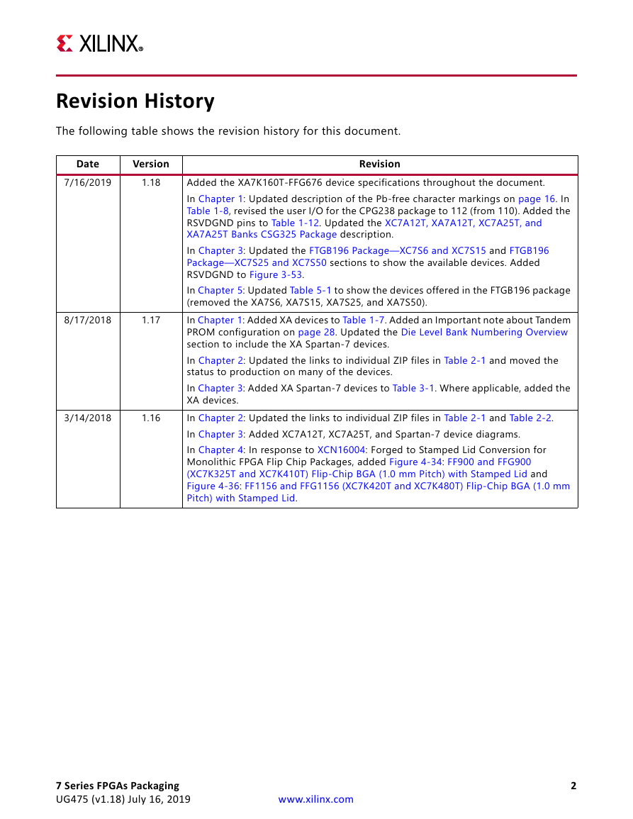
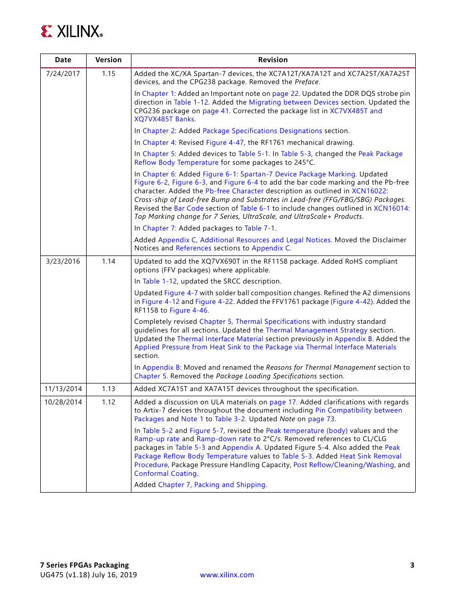
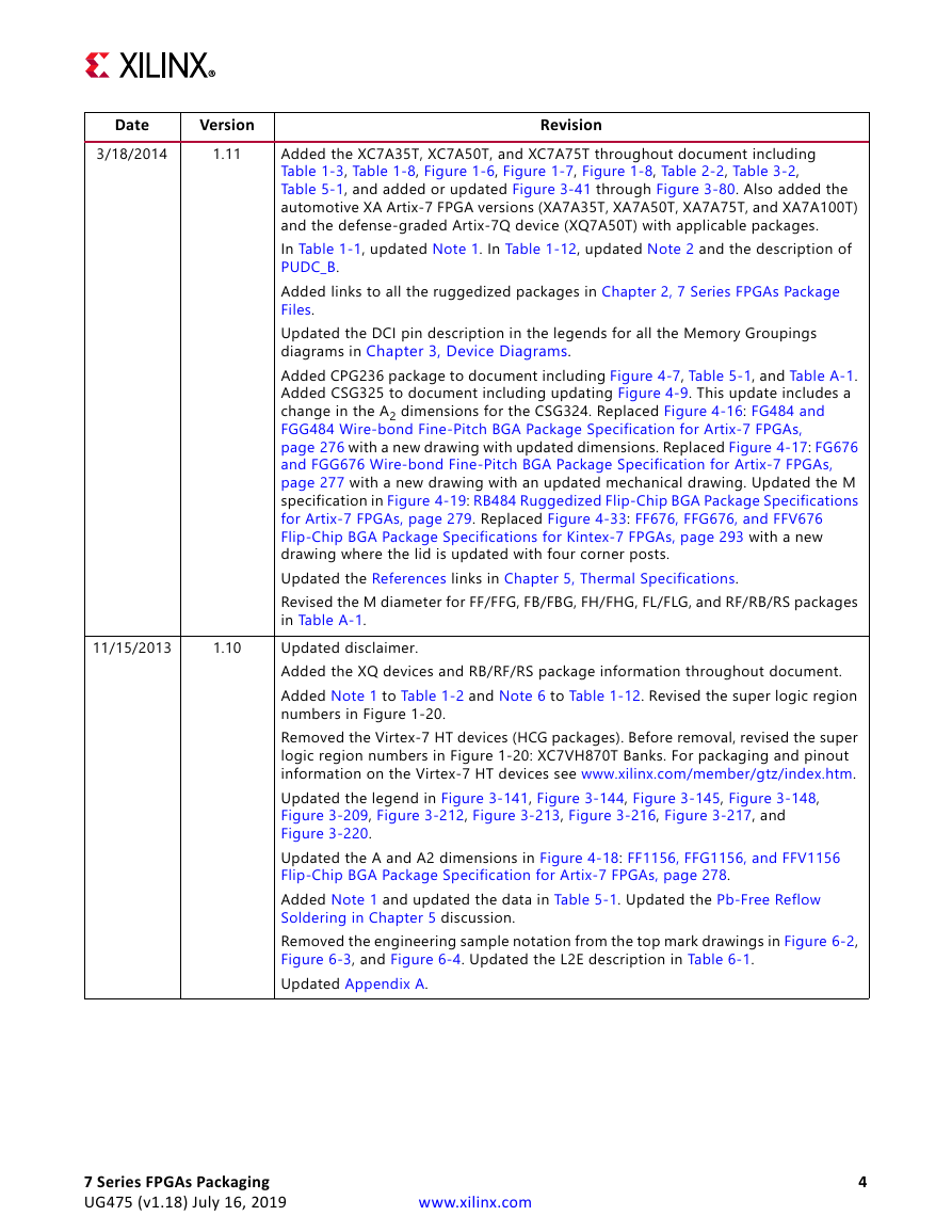
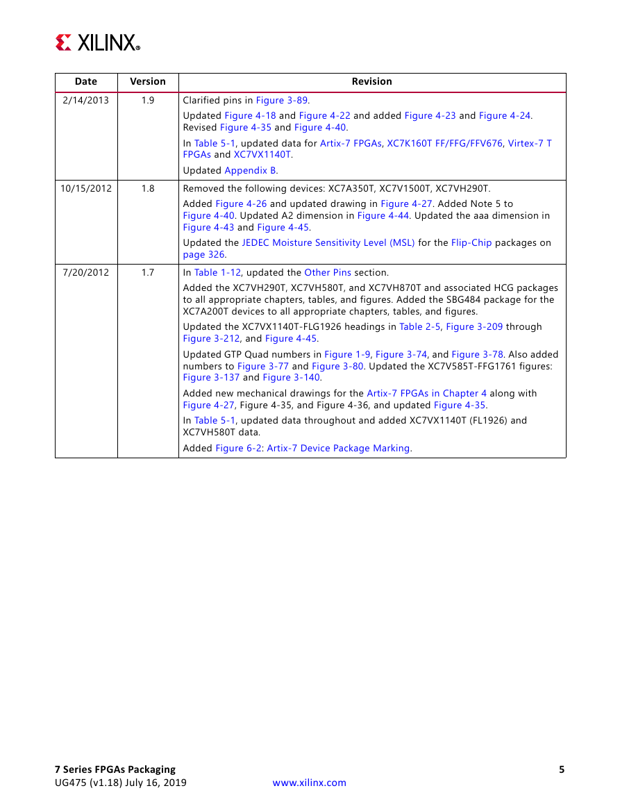
Revision History
Table of Contents
Ch. 1: Packaging Overview
About this Guide
Introduction
Device/Package Combinations and Maximum I/Os
Serial Transceiver Channels by Device/Package
User I/O Pins by Device/Package
Pin Definitions
Pin Compatibility between Packages
Migrating between Devices
Die Level Bank Numbering Overview
Banking and Clocking Summary
XC7S6, XA7S6, XC7S15, and XA7S15 Banks
FTGB196 Package
CPGA196 Package
CSGA225 Package
XC7S25 and XA7S25 Banks
FTGB196 Package
CSGA225 Package
CSGA324 Package
XC7S50 and XA7S50 Banks
FTGB196 Package
CSGA324 Package
FGGA484 Package
XC7S75, XA7S75, XC7S100, and XA7S100 Banks
FGGA484 Package
FGGA676 Package
XC7A12T, XA7A12T, XC7A25T, and XA7A25T Banks
CPG238 Package
CSG325 Package
XC7A15T, XC7A35T, XA7A15T, and XA7A35T Banks
CPG236 Package
FTG256 Package (XC7A15T and XC7A35T only)
CSG324 Package
CSG325 Package
FGG484 Package (XC7A15T and XC7A35T only)
XC7A50T, XA7A50T, and XQ7A50T Banks
CPG236 Package
FTG256 Package (XC7A50T only)
CSG324 Package
CSG325 Package
FGG484 Package (XC7A50T and XQ7A50T only)
XC7A75T and XA7A75T Banks
FTG256 Package (XC7A75T only)
CSG324 Package
FGG484 Package
FGG676 Package (XC7A75T only)
XC7A100T, XQ7A100T, and XA7A100T Banks
FTG256 Package (XC7A100T only)
CSG324 Package
FGG484 Package
FGG676 Package (XC7A100T only)
XC7A200T and XQ7A200T Banks
SBG484, SBV484, and RS484 Packages
FBG484, FBV484, and RB484 Packages
FBG676, FBV676, and RB676 Packages
FFG1156 and FFV1156 Package (XC7A200T only)
XC7K70T Banks
FBG484 and FBV484 Package
FBG676 and FBV676 Package
XC7K160T and XA7K160T Banks
FBG484 and FBV484 Package
FBG676, FBV676, FFG676, and FFV676 Packages
XC7K325T and XQ7K325T Banks
FBG676, FBV676, FFG676, FFV676, and RF676 Packages
FBG900, FBV900, FFG900, FFV900, and RF900 Packages
XC7K355T Banks
FFG901 and FFV901 Package
XC7K410T and XQ7K410T Banks
FBG676, FBV676, FFG676, FFV676, and RF676 Packages
FBG900, FBV900, FFG900, FFV900, and RF900 Packages
XC7K420T Banks
FFG901 and FFV901 Package
FFG1156 and FFV1156 Package
XC7K480T Banks
FFG901 and FFV901 Package
FFG1156 and FFV1156 Package
XC7V585T and XQ7V585T Banks
FFG1157 and RF1157 Packages
FFG1761 and RF1761 Packages
XC7V2000T Banks
FHG1761 Package
FLG1925 Package
XC7VX330T and XQ7VX330T Banks
FFG1157, FFV1157, and RF1157 Packages
FFG1761, FFV1761, and RF1761 Packages
XC7VX415T Banks
FFG1157 and FFV1157 Package
FFG1158 and FFV1158 Package
FFG1927 and FFV1927 Package
XC7VX485T and XQ7VX485T Banks
FFG1157 Package
FFG1158 Packages
FFG1761 and RF1761 Packages
FFG1927 Package
FFG1930 and RF1930 Packages
XC7VX550T Banks
FFG1158 Package
FFG1927 Package
XC7VX690T and XQ7VX690T Banks
FFG1157 and RF1157 Packages
FFG1158 and RF1158 Packages
FFG1761 and RF1761 Packages
FFG1926 Package
FFG1927 Package
FFG1930 and RF1930 Packages
XC7VX980T and XQ7VX980T Banks
FFG1926 Package
FFG1928 Package
FFG1930 and RF1930 Packages
XC7VX1140T Banks
FLG1926 Package
FLG1928 Package
FLG1930 Package
Ch. 2: 7 Series FPGAs Package Files
About ASCII Package Files
Package Specifications Designations
Evaluation Only
Engineering Sample
Production
ASCII Pinout Files
Ch. 3: Device Diagrams
Summary
Spartan-7 FPGAs Device Diagrams
CPGA196 Package—XC7S6, XA7S6, XC7S15, and XA7S15
FTGB196 Package—XC7S6 and XC7S15
FTGB196 Package—XC7S25 and XC7S50
CSGA225 Package—XC7S6, XC7S15, XA7S6, and XA7S15
CSGA225 Package—XC7S25 and XA7S25
CSGA324 Package—XC7S25 and XA7S25
CSGA324 Package—XC7S50 and XA7S50
FGGA484 Package—XC7S50 and XA7S50
FGGA484 Package—XC7S75, XC7S100, XA7S75, and XA7S100
FGGA676 Package—XC7S75, XC7S100, XA7S75, and XA7S100
Artix-7 FPGAs Device Diagrams
CP236 and CPG236 Packages—XC7A15T, XC7A35T, and XC7A50T CPG236 Package (only)—XA7A15T, XA7A35T, and XA7A50T
CPG238 Package—XC7A12T, XC7A25T, XA7A12T, and XA7A25T
CS324 and CSG324 Packages—XC7A15T, XC7A35T, XC7A50T, XC7A75T, and XC7A100T CSG324 Packages (only)—XA7A15T, XA7A35T, XA7A50T, XA7A75T, and XA7A100T
CSG325 Package—XC7A12T and XA7A12T
CSG325 Package—XC7A25T and XA7A25T
CS325 and CSG325 Packages—XC7A15T, XC7A35T, and XC7A50T CSG325 Packages (only)—XA7A15T, XA7A35T, and XA7A50T
FT256 and FTG256 Packages—XC7A15T, XC7A35T, XC7A50T, XC7A75T, and XC7A100T
FG484 and FGG484 Packages—XC7A15T, XC7A35T, and XC7A50T
FG484 and FGG484 Packages—XC7A75T and XC7A100T FGG484 Packages (only)—XA7A75T and XA7A100T
FG676 and FGG676 Packages—XC7A75T and XC7A100T
SB484, SBG484, SBV484, and RS484 Packages—XC7A200T
FB484, FBG484, FBV484, and RB484 Packages—XC7A200T
FB676, FBG676, FBV676, and RB676 Packages—XC7A200T
FF1156, FFG1156, and FFV1156 Packages—XC7A200T
Kintex-7 FPGAs Device Diagrams
FB484, FBG484, and FBV484 Packages—XC7K70T and XC7K160T
FB676, FBG676, and FBV676 Packages—XC7K70T
FB676, FBG676, and FBV676 Packages—XC7K160T, XC7K325T, and XC7K410T
FB900, FBG900, and FBV900 Packages—XC7K325T and XC7K410T
FF676, FFG676, FFV676, and RF676 Packages—XC7K160T, XA7K160T, XC7K325T, and XC7K410T
FF900, FFG900, FFV900, and RF900 Packages—XC7K325T and XC7K410T
FF901, FFG901, and FFV901 Packages—XC7K355T
FF901, FFG901, and FFV901 Packages—XC7K420T and XC7K480T
FF1156, FFG1156, and FFV1156 Packages—XC7K420T and XC7K480T
Virtex-7 FPGAs Device Diagrams
FF1157, FFG1157, and RF1157 Packages—XC7V585T
FF1761, FFG1761, and RF1761 Packages—XC7V585T
FL1925 and FLG1925 Packages—XC7V2000T
FH1761 and FHG1761 Packages—XC7V2000T
FF1157, FFG1157, and RF1157 Packages—XC7VX330T, XC7VX415T, and XC7VX690T
FF1761, FFG1761, and RF1761 Packages—XC7VX330T
FF1158, FFG1158, FFV1158, and RF1158 Packages—XC7VX415T, XC7VX550T, and XC7VX690T
FF1927, FFG1927, and FFV1927 Packages—XC7VX415T
FF1157, FFG1157, and FFV1157 Packages—XC7VX485T
FF1158, FFG1158, and FFV1158 Packages—XC7VX485T
FF1761, FFG1761, and RF1761 Packages—XC7VX485T
FF1927 and FFG1927 Packages—XC7VX485T
FF1930, FFG1930, and RF1930 Packages—XC7VX485T
FF1761, FFG1761, and RF1761 Packages—XC7VX690T
FF1926 and FFG1926 Packages—XC7VX690T and XC7VX980T
FF1927 and FFG1927 Packages—XC7VX550T and XC7VX690T
FF1930, FFG1930, and RF1930 Packages—XC7VX690T
FF1928 and FFG1928 Packages—XC7VX980T
FF1930, FFG1930, and RF1930 Packages—XC7VX980T
FL1926 and FLG1926 Packages—XC7VX1140T
FL1928 and FLG1928 Packages—XC7VX1140T
FL1930 and FLG1930 Packages—XC7VX1140T
Ch. 4: Mechanical Drawings
Summary
Spartan-7 FPGAs
Artix-7 FPGAs
Kintex-7 FPGAs
Virtex-7 FPGAs
CPGA196 (Spartan-7 FPGAs) Wire-Bond Chip-Scale BGA (0.5 mm Pitch)
FTGB196 (Spartan-7 FPGAs) Wire-Bond Chip-Scale BGA (1.0 mm Pitch)
CSGA225 (Spartan-7 FPGAs) Wire-Bond Chip-Scale BGA (0.8 mm Pitch)
CSGA324 (Spartan-7 FPGAs) Wire-Bond Chip-Scale BGA (0.8 mm Pitch)
FGGA484 (Spartan-7 FPGAs) Wire-Bond Fine-Pitch BGA (1.0 mm Pitch)
FGGA676 (Spartan-7 FPGAs) Wire-Bond Fine-Pitch BGA (1.0 mm Pitch)
CP236 and CPG236 (Artix-7 FPGAs) Wire-Bond Chip-Scale BGA (0.5 mm Pitch)
CPG238 (Artix-7 FPGAs: XC7A12T and XC7A25T) Wire-Bond Chip-Scale BGA (0.5 mm Pitch)
CS/CSG324 and CS/CSG325 (Artix-7 FPGAs) Wire-Bond Chip-Scale BGA (0.8 mm Pitch)
FT/FTG256 (Artix-7 FPGAs) Wire-Bond Fine-Pitch Thin BGA (1.0 mm Pitch)
SB484, SBG484, and SBV484 (Artix-7 FPGAs) Flip-Chip Lidless BGA (0.8 mm Pitch)
FB484, FBG484, and FBV484 (Artix-7 FPGAs) Flip-Chip Lidless BGA (1.0 mm Pitch)
FB676, FBG676, and FBV676 (Artix-7 FPGAs) Flip-Chip Lidless BGA (1.0 mm Pitch)
FG484 and FGG484 (Artix-7 FPGAs) Wire-Bond Fine-Pitch BGA (1.0 mm Pitch)
FG676 and FGG676 (Artix-7 FPGAs) Wire-Bond Fine-Pitch BGA (1.0 mm Pitch)
FF1156, FFG1156, and FFV1156 (Artix-7 FPGAs) Flip-Chip BGA (1.0 mm Pitch)
RB484 (Artix-7 FPGAs) Ruggedized Flip-Chip BGA (1.0 mm Pitch)
RS484 (Artix-7 FPGAs) Ruggedized Flip-Chip BGA (0.8 mm Pitch)
RB676 (Artix-7 FPGAs) Ruggedized Flip-Chip BGA (1.0 mm Pitch)
FB484, FBG484, and FBV484 (Kintex-7 FPGAs) Flip-Chip Lidless BGA (1.0 mm Pitch)
FB676, FBG676, and FBV676 (Kintex-7 FPGAs) Flip-Chip Lidless BGA (1.0 mm Pitch)
FB900, FBG900, and FBV900 (Kintex-7 FPGAs) Flip-Chip Lidless BGA (1.0 mm Pitch)
FF676, FFG676, and FFV676 (Kintex-7 FPGAs) Flip-Chip BGA (1.0 mm Pitch)
FF900 and FFG900 (XC7K325T and XC7K410T) Flip-Chip BGA (1.0 mm Pitch) with Stamped Lid
FF900, FFG900, FFV900, FF901, FFG901, and FFV901 (Kintex-7 FPGAs) Flip-Chip BGA (1.0 mm Pitch)
FF1156 and FFG1156 (XC7K420T and XC7K480T) Flip-Chip BGA (1.0 mm Pitch) with Stamped Lid
FF1156, FFG1156, and FFV1156 (Kintex-7 FPGAs) Flip-Chip BGA (1.0 mm Pitch)
RF676 (Kintex-7 FPGAs) Flip-Chip BGA (1.0 mm Pitch)
RF900 (Kintex-7 FPGAs) Flip-Chip BGA (1.0 mm Pitch)
FF1157, FFG1157, FFV1157, FF1158, FFG1158, and FFV1158 (Virtex-7 FPGAs) Flip-Chip BGA (1.0 mm Pitch)
FF1761 and FFG1761 (Virtex-7 FPGAs) Flip-Chip BGA (1.0 mm Pitch)
FFV1761 (Virtex-7 FPGAs) Flip-Chip BGA (1.0 mm Pitch)
FH1761 and FHG1761 (Virtex-7 T FPGAs) Flip-Chip BGA (1.0 mm Pitch)
FF1926, FFG1926, FF1927, FFG1927, FFV1927, FF1928, FFG1928, FF1930, and FFG1930 (Virtex-7 XT FPGAs) Flip-Chip BGA (1.0 mm Pitch)
FL1925, FLG1925, FL1926, FLG1926, FL1928, FLG1928, and FL1930, FLG1930 (Virtex-7 FPGAs) Flip-Chip BGA (1.0 mm Pitch)
RF1157 and RF1158 Flip-Chip BGA (Virtex-7 FPGAs) (1.0 mm Pitch)
RF1761 Flip-Chip BGA (Virtex-7 FPGAs) (1.0 mm Pitch)
RF1930 Flip-Chip BGA (Virtex-7 FPGAs) (1.0 mm Pitch)
Ch. 5: Thermal Specifications
Introduction
Thermal Resistance Data
Support for Thermal Models
Thermal Management Strategy
Cavity-Up Plastic BGA Packages
Wire-Bond Packages
Flip-Chip Packages
System Level Heat Sink Solutions
Thermal Interface Material
Types of TIM
Guidelines for Thermal Interface Materials
Thermal Conductivity of the Material
Electrical Conductivity of the Material
Spreading Characteristics of the Material
Long-Term Stability and Reliability of the Material
Ease of Application
Applied Pressure from Heat Sink to the Package via Thermal Interface Materials
Heat Sink Removal Procedure
Soldering Guidelines
Sn/Pb Reflow Soldering
Notes for Figure 5-6:
Pb-Free Reflow Soldering
Post Reflow/Cleaning/Washing
Conformal Coating
Ch. 6: Package Marking
Introduction
Ch. 7: Packing and Shipping
Introduction
Appx. A: Recommended PCB Design Rules for BGA Packages
BGA Packages
Appx. B: Heat Sink Guidelines for Lidless Flip-Chip Packages
Heat Sink Attachments for Lidless Flip-chip BGA (FB/FBG/FBV and SB/SBG/SBV)
Silicon and Decoupling Capacitors Height Consideration
Types of Heat Sink Attachments
Heat Sink Attachment
Component Pick-up Tool Consideration
Heat Sink Attachment Process Considerations
Standard Heat Sink Attach Process with Thermal Conductive Adhesive
Standard Heat Sink Attach Process with Thermal Adhesive Tape
Push-Pin and Shoulder Screw Heat Sink Attachment Process with Phase Change Material (PCM) Application
Appx. C: Additional Resources and Legal Notices
Xilinx Resources
Solution Centers
References
Please Read: Important Legal Notices
7 Series FPGAs Packaging and Pinout Product Specification UG475 (v1.18) July 16, 2019
Revision History The following table shows the revision history for this document. Date 7/16/2019 Version 1.18 8/17/2018 1.17 3/14/2018 1.16 Revision Added the XA7K160T-FFG676 device specifications throughout the document. In Chapter 1: Updated description of the Pb-free character markings on page 16. In Table 1-8, revised the user I/O for the CPG238 package to 112 (from 110). Added the RSVDGND pins to Table 1-12. Updated the XC7A12T, XA7A12T, XC7A25T, and XA7A25T Banks CSG325 Package description. In Chapter 3: Updated the FTGB196 Package—XC7S6 and XC7S15 and FTGB196 Package—XC7S25 and XC7S50 sections to show the available devices. Added RSVDGND to Figure 3-53. In Chapter 5: Updated Table 5-1 to show the devices offered in the FTGB196 package (removed the XA7S6, XA7S15, XA7S25, and XA7S50). In Chapter 1: Added XA devices to Table 1-7. Added an Important note about Tandem PROM configuration on page 28. Updated the Die Level Bank Numbering Overview section to include the XA Spartan-7 devices. In Chapter 2: Updated the links to individual ZIP files in Table 2-1 and moved the status to production on many of the devices. In Chapter 3: Added XA Spartan-7 devices to Table 3-1. Where applicable, added the XA devices. In Chapter 2: Updated the links to individual ZIP files in Table 2-1 and Table 2-2. In Chapter 3: Added XC7A12T, XC7A25T, and Spartan-7 device diagrams. In Chapter 4: In response to XCN16004: Forged to Stamped Lid Conversion for Monolithic FPGA Flip Chip Packages, added Figure 4-34: FF900 and FFG900 (XC7K325T and XC7K410T) Flip-Chip BGA (1.0 mm Pitch) with Stamped Lid and Figure 4-36: FF1156 and FFG1156 (XC7K420T and XC7K480T) Flip-Chip BGA (1.0 mm Pitch) with Stamped Lid. 7 Series FPGAs Packaging UG475 (v1.18) July 16, 2019 www.xilinx.com 2
Date 7/24/2017 Version 1.15 3/23/2016 1.14 11/13/2014 10/28/2014 1.13 1.12 Revision Added the XC/XA Spartan-7 devices, the XC7A12T/XA7A12T and XC7A25T/XA7A25T devices, and the CPG238 package. Removed the Preface. In Chapter 1: Added an Important note on page 22. Updated the DDR DQS strobe pin direction in Table 1-12. Added the Migrating between Devices section. Updated the CPG236 package on page 41. Corrected the package list in XC7VX485T and XQ7VX485T Banks. In Chapter 2: Added Package Specifications Designations section. In Chapter 4: Revised Figure 4-47, the RF1761 mechanical drawing. In Chapter 5: Added devices to Table 5-1. In Table 5-3, changed the Peak Package Reflow Body Temperature for some packages to 245°C. In Chapter 6: Added Figure 6-1: Spartan-7 Device Package Marking. Updated Figure 6-2, Figure 6-3, and Figure 6-4 to add the bar code marking and the Pb-free character. Added the Pb-free Character description as outlined in XCN16022: Cross-ship of Lead-free Bump and Substrates in Lead-free (FFG/FBG/SBG) Packages. Revised the Bar Code section of Table 6-1 to include changes outlined in XCN16014: Top Marking change for 7 Series, UltraScale, and UltraScale+ Products. In Chapter 7: Added packages to Table 7-1. Added Appendix C, Additional Resources and Legal Notices. Moved the Disclaimer Notices and References sections to Appendix C. Updated to add the XQ7VX690T in the RF1158 package. Added RoHS compliant options (FFV packages) where applicable. In Table 1-12, updated the SRCC description. Updated Figure 4-7 with solder ball composition changes. Refined the A2 dimensions in Figure 4-12 and Figure 4-22. Added the FFV1761 package (Figure 4-42). Added the RF1158 to Figure 4-46. Completely revised Chapter 5, Thermal Specifications with industry standard guidelines for all sections. Updated the Thermal Management Strategy section. Updated the Thermal Interface Material section previously in Appendix B. Added the Applied Pressure from Heat Sink to the Package via Thermal Interface Materials section. In Appendix B: Moved and renamed the Reasons for Thermal Management section to Chapter 5. Removed the Package Loading Specifications section. Added XC7A15T and XA7A15T devices throughout the specification. Added a discussion on ULA materials on page 17. Added clarifications with regards to Artix-7 devices throughout the document including Pin Compatibility between Packages and Note 1 to Table 3-2. Updated Note on page 73. In Table 5-2 and Figure 5-7, revised the Peak temperature (body) values and the Ramp-up rate and Ramp-down rate to 2°C/s. Removed references to CL/CLG packages in Table 5-3 and Appendix A. Updated Figure 5-4. Also added the Peak Package Reflow Body Temperature values to Table 5-3. Added Heat Sink Removal Procedure, Package Pressure Handling Capacity, Post Reflow/Cleaning/Washing, and Conformal Coating. Added Chapter 7, Packing and Shipping. 7 Series FPGAs Packaging UG475 (v1.18) July 16, 2019 www.xilinx.com 3
Date 3/18/2014 Version 1.11 11/15/2013 1.10 Revision Added the XC7A35T, XC7A50T, and XC7A75T throughout document including Table 1-3, Table 1-8, Figure 1-6, Figure 1-7, Figure 1-8, Table 2-2, Table 3-2, Table 5-1, and added or updated Figure 3-41 through Figure 3-80. Also added the automotive XA Artix-7 FPGA versions (XA7A35T, XA7A50T, XA7A75T, and XA7A100T) and the defense-graded Artix-7Q device (XQ7A50T) with applicable packages. In Table 1-1, updated Note 1. In Table 1-12, updated Note 2 and the description of PUDC_B. Added links to all the ruggedized packages in Chapter 2, 7 Series FPGAs Package Files. Updated the DCI pin description in the legends for all the Memory Groupings diagrams in Chapter 3, Device Diagrams. Added CPG236 package to document including Figure 4-7, Table 5-1, and Table A-1. Added CSG325 to document including updating Figure 4-9. This update includes a change in the A2 dimensions for the CSG324. Replaced Figure 4-16: FG484 and FGG484 Wire-bond Fine-Pitch BGA Package Specification for Artix-7 FPGAs, page 276 with a new drawing with updated dimensions. Replaced Figure 4-17: FG676 and FGG676 Wire-bond Fine-Pitch BGA Package Specification for Artix-7 FPGAs, page 277 with a new drawing with an updated mechanical drawing. Updated the M specification in Figure 4-19: RB484 Ruggedized Flip-Chip BGA Package Specifications for Artix-7 FPGAs, page 279. Replaced Figure 4-33: FF676, FFG676, and FFV676 Flip-Chip BGA Package Specifications for Kintex-7 FPGAs, page 293 with a new drawing where the lid is updated with four corner posts. Updated the References links in Chapter 5, Thermal Specifications. Revised the M diameter for FF/FFG, FB/FBG, FH/FHG, FL/FLG, and RF/RB/RS packages in Table A-1. Updated disclaimer. Added the XQ devices and RB/RF/RS package information throughout document. Added Note 1 to Table 1-2 and Note 6 to Table 1-12. Revised the super logic region numbers in Figure 1-20. Removed the Virtex-7 HT devices (HCG packages). Before removal, revised the super logic region numbers in Figure 1-20: XC7VH870T Banks. For packaging and pinout information on the Virtex-7 HT devices see www.xilinx.com/member/gtz/index.htm. Updated the legend in Figure 3-141, Figure 3-144, Figure 3-145, Figure 3-148, Figure 3-209, Figure 3-212, Figure 3-213, Figure 3-216, Figure 3-217, and Figure 3-220. Updated the A and A2 dimensions in Figure 4-18: FF1156, FFG1156, and FFV1156 Flip-Chip BGA Package Specification for Artix-7 FPGAs, page 278. Added Note 1 and updated the data in Table 5-1. Updated the Pb-Free Reflow Soldering in Chapter 5 discussion. Removed the engineering sample notation from the top mark drawings in Figure 6-2, Figure 6-3, and Figure 6-4. Updated the L2E description in Table 6-1. Updated Appendix A. 7 Series FPGAs Packaging UG475 (v1.18) July 16, 2019 www.xilinx.com 4
Date 2/14/2013 Version 1.9 10/15/2012 1.8 7/20/2012 1.7 Revision Clarified pins in Figure 3-89. Updated Figure 4-18 and Figure 4-22 and added Figure 4-23 and Figure 4-24. Revised Figure 4-35 and Figure 4-40. In Table 5-1, updated data for Artix-7 FPGAs, XC7K160T FF/FFG/FFV676, Virtex-7 T FPGAs and XC7VX1140T. Updated Appendix B. Removed the following devices: XC7A350T, XC7V1500T, XC7VH290T. Added Figure 4-26 and updated drawing in Figure 4-27. Added Note 5 to Figure 4-40. Updated A2 dimension in Figure 4-44. Updated the aaa dimension in Figure 4-43 and Figure 4-45. Updated the JEDEC Moisture Sensitivity Level (MSL) for the Flip-Chip packages on page 326. In Table 1-12, updated the Other Pins section. Added the XC7VH290T, XC7VH580T, and XC7VH870T and associated HCG packages to all appropriate chapters, tables, and figures. Added the SBG484 package for the XC7A200T devices to all appropriate chapters, tables, and figures. Updated the XC7VX1140T-FLG1926 headings in Table 2-5, Figure 3-209 through Figure 3-212, and Figure 4-45. Updated GTP Quad numbers in Figure 1-9, Figure 3-74, and Figure 3-78. Also added numbers to Figure 3-77 and Figure 3-80. Updated the XC7V585T-FFG1761 figures: Figure 3-137 and Figure 3-140. Added new mechanical drawings for the Artix-7 FPGAs in Chapter 4 along with Figure 4-27, Figure 4-35, and Figure 4-36, and updated Figure 4-35. In Table 5-1, updated data throughout and added XC7VX1140T (FL1926) and XC7VH580T data. Added Figure 6-2: Artix-7 Device Package Marking. 7 Series FPGAs Packaging UG475 (v1.18) July 16, 2019 www.xilinx.com 5
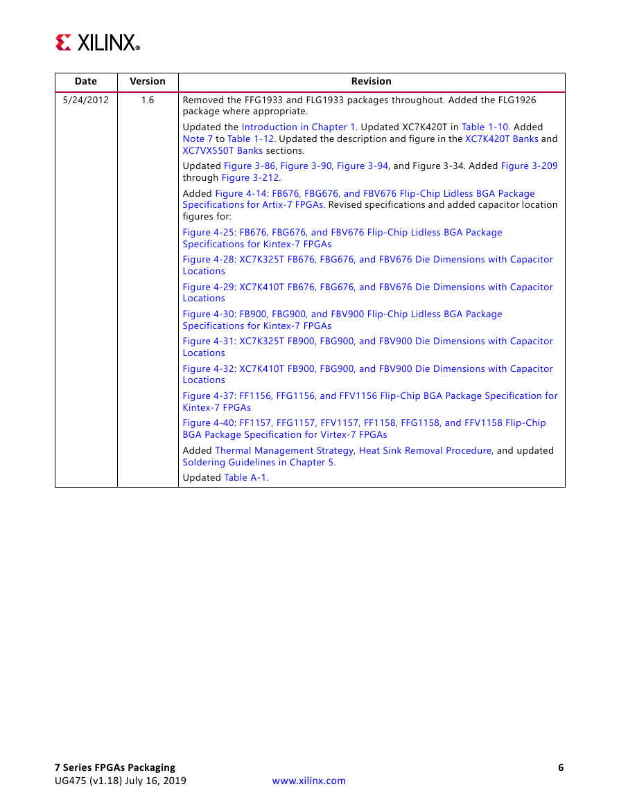
Date 5/24/2012 Version 1.6 Revision Removed the FFG1933 and FLG1933 packages throughout. Added the FLG1926 package where appropriate. Updated the Introduction in Chapter 1. Updated XC7K420T in Table 1-10. Added Note 7 to Table 1-12. Updated the description and figure in the XC7K420T Banks and XC7VX550T Banks sections. Updated Figure 3-86, Figure 3-90, Figure 3-94, and Figure 3-34. Added Figure 3-209 through Figure 3-212. Added Figure 4-14: FB676, FBG676, and FBV676 Flip-Chip Lidless BGA Package Specifications for Artix-7 FPGAs. Revised specifications and added capacitor location figures for: Figure 4-25: FB676, FBG676, and FBV676 Flip-Chip Lidless BGA Package Specifications for Kintex-7 FPGAs Figure 4-28: XC7K325T FB676, FBG676, and FBV676 Die Dimensions with Capacitor Locations Figure 4-29: XC7K410T FB676, FBG676, and FBV676 Die Dimensions with Capacitor Locations Figure 4-30: FB900, FBG900, and FBV900 Flip-Chip Lidless BGA Package Specifications for Kintex-7 FPGAs Figure 4-31: XC7K325T FB900, FBG900, and FBV900 Die Dimensions with Capacitor Locations Figure 4-32: XC7K410T FB900, FBG900, and FBV900 Die Dimensions with Capacitor Locations Figure 4-37: FF1156, FFG1156, and FFV1156 Flip-Chip BGA Package Specification for Kintex-7 FPGAs Figure 4-40: FF1157, FFG1157, FFV1157, FF1158, FFG1158, and FFV1158 Flip-Chip BGA Package Specification for Virtex-7 FPGAs Added Thermal Management Strategy, Heat Sink Removal Procedure, and updated Soldering Guidelines in Chapter 5. Updated Table A-1. 7 Series FPGAs Packaging UG475 (v1.18) July 16, 2019 www.xilinx.com 6
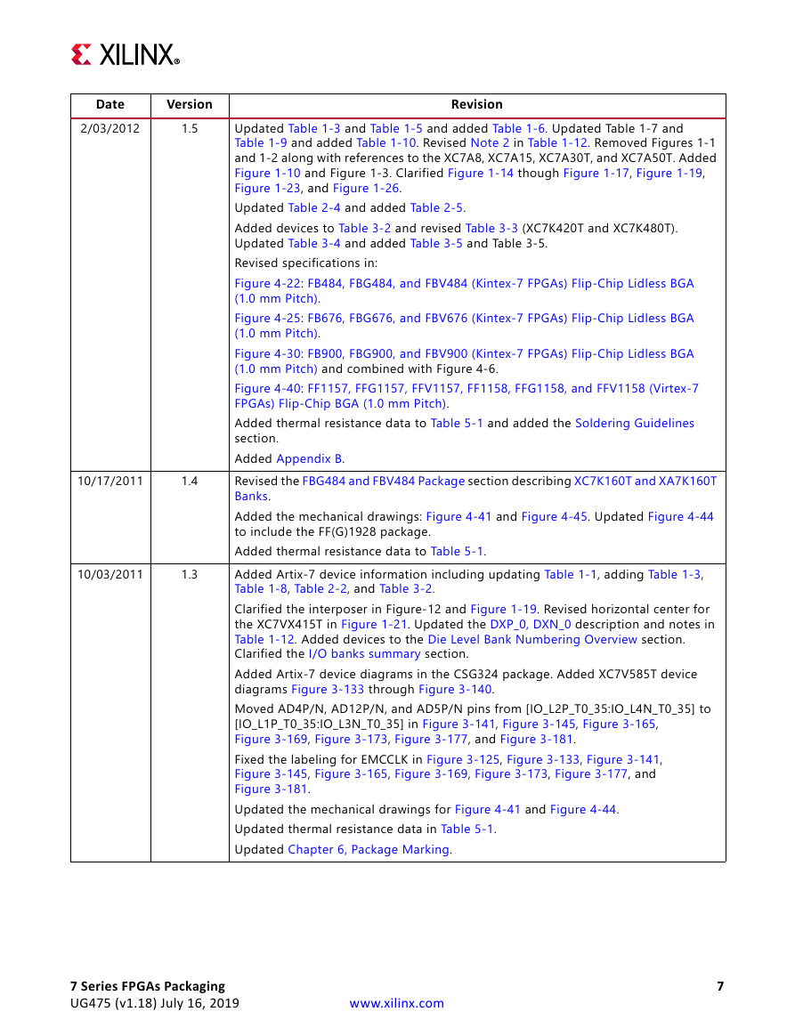
Date 2/03/2012 Version 1.5 10/17/2011 1.4 10/03/2011 1.3 Revision Updated Table 1-3 and Table 1-5 and added Table 1-6. Updated Table 1-7 and Table 1-9 and added Table 1-10. Revised Note 2 in Table 1-12. Removed Figures 1-1 and 1-2 along with references to the XC7A8, XC7A15, XC7A30T, and XC7A50T. Added Figure 1-10 and Figure 1-3. Clarified Figure 1-14 though Figure 1-17, Figure 1-19, Figure 1-23, and Figure 1-26. Updated Table 2-4 and added Table 2-5. Added devices to Table 3-2 and revised Table 3-3 (XC7K420T and XC7K480T). Updated Table 3-4 and added Table 3-5 and Table 3-5. Revised specifications in: Figure 4-22: FB484, FBG484, and FBV484 (Kintex-7 FPGAs) Flip-Chip Lidless BGA (1.0 mm Pitch). Figure 4-25: FB676, FBG676, and FBV676 (Kintex-7 FPGAs) Flip-Chip Lidless BGA (1.0 mm Pitch). Figure 4-30: FB900, FBG900, and FBV900 (Kintex-7 FPGAs) Flip-Chip Lidless BGA (1.0 mm Pitch) and combined with Figure 4-6. Figure 4-40: FF1157, FFG1157, FFV1157, FF1158, FFG1158, and FFV1158 (Virtex-7 FPGAs) Flip-Chip BGA (1.0 mm Pitch). Added thermal resistance data to Table 5-1 and added the Soldering Guidelines section. Added Appendix B. Revised the FBG484 and FBV484 Package section describing XC7K160T and XA7K160T Banks. Added the mechanical drawings: Figure 4-41 and Figure 4-45. Updated Figure 4-44 to include the FF(G)1928 package. Added thermal resistance data to Table 5-1. Added Artix-7 device information including updating Table 1-1, adding Table 1-3, Table 1-8, Table 2-2, and Table 3-2. Clarified the interposer in Figure-12 and Figure 1-19. Revised horizontal center for the XC7VX415T in Figure 1-21. Updated the DXP_0, DXN_0 description and notes in Table 1-12. Added devices to the Die Level Bank Numbering Overview section. Clarified the I/O banks summary section. Added Artix-7 device diagrams in the CSG324 package. Added XC7V585T device diagrams Figure 3-133 through Figure 3-140. Moved AD4P/N, AD12P/N, and AD5P/N pins from [IO_L2P_T0_35:IO_L4N_T0_35] to [IO_L1P_T0_35:IO_L3N_T0_35] in Figure 3-141, Figure 3-145, Figure 3-165, Figure 3-169, Figure 3-173, Figure 3-177, and Figure 3-181. Fixed the labeling for EMCCLK in Figure 3-125, Figure 3-133, Figure 3-141, Figure 3-145, Figure 3-165, Figure 3-169, Figure 3-173, Figure 3-177, and Figure 3-181. Updated the mechanical drawings for Figure 4-41 and Figure 4-44. Updated thermal resistance data in Table 5-1. Updated Chapter 6, Package Marking. 7 Series FPGAs Packaging UG475 (v1.18) July 16, 2019 www.xilinx.com 7
Date 6/14/2011 Version 1.2 4/06/2011 1.1 3/01/2011 1.0 Revision Added Virtex-7 device information including updating Table 1-1, adding Table 1-3, Table 1-10, Table 2-4, and Table 3-4. In Table 1-12, updated Note 3, the Configuration Pins section, and the Analog to Digital Converter (XADC) Pins section. Updated Figure 3-99, Figure 3-100, Figure 3-103, Figure 3-104, Figure 3-107, Figure 3-108, Figure 3-111, Figure 3-112, Figure 3-115, Figure 3-116, Figure 3-119, and Figure 3-120. Added Figure 3-120 through Figure 3-184. Added Figure 4-37 the mechanical drawing for the Kintex-7 devices FFG1156 package. Also added some Virtex-7 device mechanical drawings in Figure 4-37 through Figure 4-44. Added thermal resistance data to Table 5-1. Removed the SBG324 package from the entire document. Added three Kintex®-7 devices: XC7K355T, XC7K420T, and XC7K480T. Updated disclaimer and copyright on page 343. Updated package size of FF1156 in Table 1-1. Updated DXP_0, DXN_0 in Table 1-12. The Table 2-3 single ASCII device files have been updated for both the XC7K70T and XC7K160T. All ASCII TXT files and the overall ZIP file have been updated on the web. Updated the XC7K70TFBG676 figures: Figure 3-101, Figure 3-102, Figure 3-103, and Figure 3-104. Added information to Chapter 4, Mechanical Drawings, Chapter 5, Thermal Specifications, and Chapter 6, Package Marking. Initial Xilinx release. 7 Series FPGAs Packaging UG475 (v1.18) July 16, 2019 www.xilinx.com 8
分享到:
收藏