ASSOCIATION CONNECTING
ELECTRONICS INDUSTRIES
IPC-SM-782A
Includes: Amendment 1 and 2
Surface Mount Design and
Land Pattern Standard
IPC-SM-782A
August 1993
Amendment 1
October 1996
Amendment 2
April 1999
A standard developed by IPC
2215 Sanders Road, Northbrook, IL 60062-6135
Tel. 847.509.9700 Fax 847.509.9798
www.ipc.org
�
The Principles of
Standardization
In May 1995 the IPC’s Technical Activities Executive Committee adopted Principles of
Standardization as a guiding principle of IPC’s standardization efforts.
Notice
Standards Should:
Show relationship to Design for Manufacturability
(DFM) and Design for the Environment (DFE)
Minimize time to market
Contain simple (simplified) language
Just include spec information
Focus on end product performance
Include a feedback system on use and
problems for future improvement
Standards Should Not:
Inhibit innovation
Increase time-to-market
Keep people out
Increase cycle time
Tell you how to make something
Contain anything that cannot
be defended with data
IPC Standards and Publications are designed to serve the public interest through eliminating
misunderstandings between manufacturers and purchasers, facilitating interchangeability and
improvement of products, and assisting the purchaser in selecting and obtaining with minimum
delay the proper product for his particular need. Existence of such Standards and Publications
shall not in any respect preclude any member or nonmember of IPC from manufacturing or sell-
ing products not conforming to such Standards and Publication, nor shall the existence of such
Standards and Publications preclude their voluntary use by those other than IPC members,
whether the standard is to be used either domestically or internationally.
Recommended Standards and Publications are adopted by IPC without regard to whether their
adoption may involve patents on articles, materials, or processes. By such action, IPC does
not assume any liability to any patent owner, nor do they assume any obligation whatever to
parties adopting the Recommended Standard or Publication. Users are also wholly responsible
for protecting themselves against all claims of liabilities for patent infringement.
IPC Position
Statement on
Specification
Revision Change
It is the position of IPC’s Technical Activities Executive Committee (TAEC) that the use and
implementation of IPC publications is voluntary and is part of a relationship entered into by
customer and supplier. When an IPC standard/guideline is updated and a new revision is pub-
lished, it is the opinion of the TAEC that the use of the new revision as part of an existing
relationship is not automatic unless required by the contract. The TAEC recommends the use
of the lastest revision.
Adopted October 6. 1998
Why is there
a charge for
this standard?
Your purchase of this document contributes to the ongoing development of new and updated
industry standards. Standards allow manufacturers, customers, and suppliers to understand one
another better. Standards allow manufacturers greater efficiencies when they can set up their
processes to meet industry standards, allowing them to offer their customers lower costs.
IPC spends hundreds of thousands of dollars annually to support IPC’s volunteers in the
standards development process. There are many rounds of drafts sent out for review and
the committees spend hundreds of hours in review and development. IPC’s staff attends and
participates in committee activities, typesets and circulates document drafts, and follows all
necessary procedures to qualify for ANSI approval.
IPC’s membership dues have been kept low in order to allow as many companies as possible
to participate. Therefore, the standards revenue is necessary to complement dues revenue. The
price schedule offers a 50% discount to IPC members. If your company buys IPC standards,
why not take advantage of this and the many other benefits of IPC membership as well? For
more information on membership in IPC, please visit www.ipc.org or call 847/790-5372.
Thank you for your continued support.
©Copyright 1999. IPC, Northbrook, Illinois. All rights reserved under both international and Pan-American copyright conventions. Any
copying, scanning or other reproduction of these materials without the prior written consent of the copyright holder is strictly prohibited and
constitutes infringement under the Copyright Law of the United States.
�
IPC-SM-782A
ASSOCIATION CONNECTING
ELECTRONICS INDUSTRIES
Surface Mount Design
and Land Pattern
Standard
Developed by the Surface Mount Land Patterns Subcommittee (1-13)
of the Printed Board Design Committee (1-10) of IPC
Users of this standard are encouraged to participate in the
development of future revisions.
Contact:
IPC
2215 Sanders Road
Northbrook, Illinois
60062-6135
Tel 847 509.9700
Fax 847 509.9798
�
IPC-SM-782A
December 1999
Acknowledgment
Any Standard involving a complex technology draws material from a vast number of sources. While the principal members
of the IPC Surface Mount Land Patterns Subcommittee of the Printed Board Design Committee are shown below, it is not
possible to include all of those who assisted in the evolution of this Standard. To each of them, the members of the IPC
extend their gratitude.
Printed Board Design
Committee
Surface Mount Land Patterns
Subcommittee
Technical Liaison of the
IPC Board of Directors
Chairman
Joe Fjelstad
Tessera Inc.
Chairman
Nick Mescia
General Dynamics
Advanced Technology
Stan Gentry
Noble Industries Ltd.
Surface Mount Land Patterns Subcommittee
Anderson, R., AT&T Interconnect
Center of Excellence
Edwards, W.J., Lucent Technologies
Inc.
Artaki, I., Lucent Technologies Inc.
Baker, R.J., Central Texas Electronics
Association (CTEA)
Eldan, E., Orbotech Inc.
Engelmaier, W., Engelmaier
Associates Inc.
Banks, S., Trimble Navigation
Barlow, M., Lytton Inc.
Belin, J., Automata Inc.
Berkman, E., Excalibur Systems Inc.
Bittle, D.W., Raytheon Aircraft
Company
Boerdner, R.W., EJE Research
Bourque, J., Shure Brothers Inc.
Brydges, P., Panametrics Inc.
Burg, J.S., 3M Company
Cash, A.S., Northrop Grumman
Corporation
Caterina, J., Northrop Grumman
Corporation
Clifton, L., Intel Corporation
Cohen, L., Formation Inc.
Collins, S., Texscan Corporation
Couble, E.C., Shipley Co.
Coucher, M.M., Sequent Computer
Systems Inc.
Crowley, B., Hewlett Packard
Laboratories
D’Andrade, D., The Surface Mount
Technology Centre Inc.
Daugherty, D., Siemens Energy &
Automation
Davy, J., Northrop Grumman
Electronic Sensors & Systems Div
Dieffenbacher, W.C., Lockheed
Martin Corporation
DiFranza, M.J., The Mitre Corp.
Dolence, C., Tektronix Board Build
Operation
Feldmesser, H.S., Johns Hopkins
University
Firestein, I., Tadiran Telecom Group
Freedman, M.G., Amp Inc.
Giardina, J., Miteq Inc.
Grannells, R.T., United Technologies
Gray, B.W., Bull Electronics
Gray, F.L., Texas Instruments Inc.
Hargreaves, L., DC. Scientific Inc.
Hartsgrove, M., I-CON Industries
Inc.
Hastings, D.W., Lockheed Martin
Aeronutronic
Heath, B., TMD (Technology
Manufacturing Inc.)
Hersey, R.J., Ralph Hersey &
Associates
Hinton, P.E., Hinton PWB
Engineering
Holland, D.L., Sanders, A Lockheed
Martin Co.
Horton, R.N., Northrop Grumman
Electronic Sensors & Systems Div
Humpal, T.L., O.E.M. Worldwide
Hymes, L., The Complete Connection
Jawitz, M.W., Eimer Company
Johnson, B., Pacific Testing
Laboratories, Inc.
Johnson, K.L., Hexacon Electric
Company
Kemp, C.A., Lockheed Martin
Corporation
Kenyon, W.G., Global Centre for
Process Change
Knapp, C.W., Litton Guidance &
Control Systems
Koebert, M., Eaton Corp.
Korf, D.W., Zycon Corporation
Korth, C.M., Hibbing Electronics
Corp.
Kotecki, G.T., Northrop Grumman
Corporation
Lambert, L.P., EPTAC Corporation
Landolt, R.H., Enthone-OMI Inc.
Maguire, J.F., Boeing Defense &
Space Group
Malanchuk, D.J., Eastman Kodak Co.
KAD
Malewicz, W.R., Siemens Medical
Electronics
Mather, J.C., Rockwell International
Metcalf, R.J., Morton Electronic
Materials
Miller, R.F., Lockheed Martin
Corporation
MiLosh, D., LTX Corporation
Miosi, D., Toppan West Inc.
Morton, J.H., Lockheed Martin
Federal Systems
Murray, J.L., Clark-Schwebel Inc.
Norton, J.S., Tektronix Inc.
Officer, R., Sanders, A Lockheed
Martin Co.
Payne, C.W., Merix Corporation
Payne, J.R., Molex Electronics Ltd.
Pham, H., Symbol Technologies Inc.
Pope, D., Intel Corporation
Porter, C., Newbridge Networks
Corporation
Prachanronarong, K., GTE CSD
Prasad, R., Ray Prasad Consultancy
Group
Easterling, T., SCI Systems Inc.
Kern, T., Axiom Electronics, Inc.
Rassai, D., 3COM Corporation
ii
�
December 1999
Riesenbeck, J., Lytton Inc.
Rietdorf, B.C., Hughes Defense
Communications
Rudy, D., Lucent Technologies Inc.
Rumps, D.W., Lucent Technologies
Inc.
Russell, R., Texas Instruments Inc.
Seltzer, M.L., Hughes Delco Systems
Operations
Siegel, E.S., Pace Inc.
Skelly, H., Boeing Defense & Space
Group
Smith, E., Lucent Technologies Inc.
Socolowski, N., Alpha Metals Inc.
Solberg, V., Tessera Inc.
Stepp, L., Whittaker Electronic
Systems
Special Note of Appreciation
A special note of appreciation goes to
the following principle members of
the committee who led the effort to
make this document possible.
Theiler, G.P., Fluke Corporation
Theroux, G., Honeywell Inc.
Thompson, R.T., Loctite Corporation
Thrasher, H.M., Shipley Co.
Torres, S., Corlund Electronics Corp.
Treutler, L.E., Fachverband
Elektronik Design e.V.
Turbini, L.J., Georgia Institute of
Technology
Vanech, R., Northrop Grumman
Norden Systems
Vaught, J., Hughes Aircraft Co.
Virmani, N., NASA/Goddard Space
Flight Center
Vollmar, E.L, Methode Electronics
Inc.
IPC-SM-782A
Weiner, E.M., Weiner & Associates
Inc.
Weiner, M., Tadiran Telecom Group
White, T.M., Boeing Defense &
Space Group
Williams, J.J., Smiths Industries
Wingate, P., Amkor Electronics Inc.
Winslow, H., SCI Systems Inc.
Wood, M., The Surface Mount
Technology Centre Inc.
Woodhouse, G.P., Micron Custom
Mfg. Services Inc.
Wooldridge, J.R., Rockwell
International
Wu, F.B., Hughes Aircraft Co.
John Biancini, Advanced Flex
Gary Ferrari, IPC
Cynthia Jonas, Pitney Bowes
Vern Solberg, Tessera Inc.
Vivian Vosburg, Pac-El
Cover art by:
IPC Designers Council
William Burt
Custom Photo and Design, Inc.
iii
�
December 1999
IPC-SM-782A
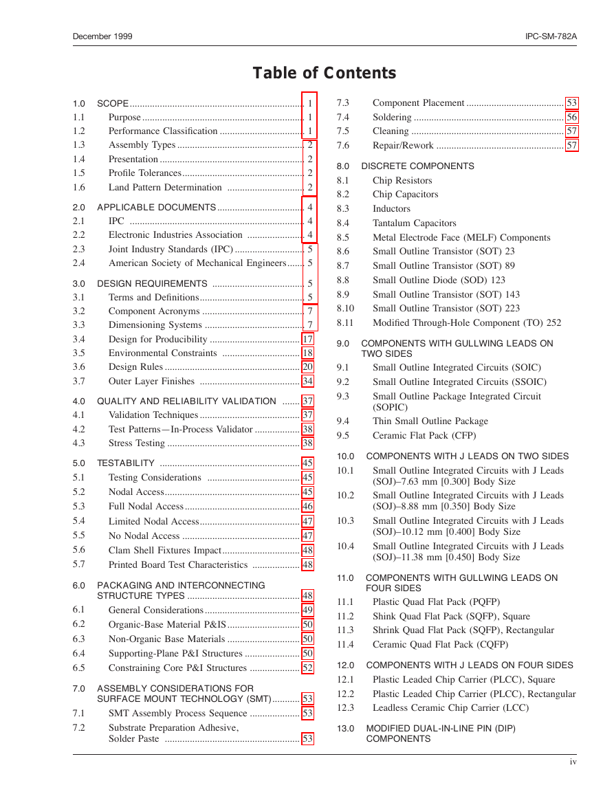
Table of Contents
1.0 SCOPE...................................................................... 1
Purpose................................................................. 1
1.1
1.2
Performance Classification .................................. 1
Assembly Types ................................................... 2
1.3
Presentation .......................................................... 2
1.4
1.5
Profile Tolerances................................................. 2
Land Pattern Determination ............................... 2
1.6
2.0 APPLICABLE DOCUMENTS................................... 4
IPC ...................................................................... 4
2.1
2.2
Electronic Industries Association ....................... 4
Joint Industry Standards (IPC) ............................ 5
2.3
2.4
American Society of Mechanical Engineers....... 5
3.0 DESIGN REQUIREMENTS ..................................... 5
Terms and Definitions.......................................... 5
3.1
Component Acronyms ......................................... 7
3.2
3.3
Dimensioning Systems ........................................ 7
Design for Producibility .................................... 17
3.4
Environmental Constraints ............................... 18
3.5
Design Rules ...................................................... 20
3.6
3.7
Outer Layer Finishes ........................................ 34
4.0 QUALITY AND RELIABILITY VALIDATION ....... 37
Validation Techniques........................................ 37
4.1
4.2
Test Patterns—In-Process Validator .................. 38
Stress Testing ..................................................... 38
4.3
5.0
5.1
5.2
5.3
5.4
5.5
5.6
5.7
TESTABILITY ........................................................ 45
Testing Considerations ..................................... 45
Nodal Access...................................................... 45
Full Nodal Access.............................................. 46
Limited Nodal Access........................................ 47
No Nodal Access ............................................... 47
Clam Shell Fixtures Impact............................... 48
Printed Board Test Characteristics ................... 48
6.0 PACKAGING AND INTERCONNECTING
STRUCTURE TYPES ............................................. 48
General Considerations...................................... 49
Organic-Base Material P&IS............................. 50
Non-Organic Base Materials ............................. 50
Supporting-Plane P&I Structures ...................... 50
Constraining Core P&I Structures .................... 52
6.1
6.2
6.3
6.4
6.5
7.1
7.2
7.0 ASSEMBLY CONSIDERATIONS FOR
SURFACE MOUNT TECHNOLOGY (SMT)........... 53
SMT Assembly Process Sequence .................... 53
Substrate Preparation Adhesive,
Solder Paste ...................................................... 53
7.3
7.4
7.5
7.6
Component Placement ....................................... 53
Soldering ............................................................ 56
Cleaning ............................................................. 57
Repair/Rework ................................................... 57
8.0 DISCRETE COMPONENTS
8.1
8.2
8.3
8.4
8.5
8.6
8.7
8.8
8.9
8.10
8.11
Chip Resistors
Chip Capacitors
Inductors
Tantalum Capacitors
Metal Electrode Face (MELF) Components
Small Outline Transistor (SOT) 23
Small Outline Transistor (SOT) 89
Small Outline Diode (SOD) 123
Small Outline Transistor (SOT) 143
Small Outline Transistor (SOT) 223
Modified Through-Hole Component (TO) 252
9.0 COMPONENTS WITH GULLWING LEADS ON
TWO SIDES
9.1
9.2
9.3
9.4
9.5
Small Outline Integrated Circuits (SOIC)
Small Outline Integrated Circuits (SSOIC)
Small Outline Package Integrated Circuit
(SOPIC)
Thin Small Outline Package
Ceramic Flat Pack (CFP)
10.2
10.0 COMPONENTS WITH J LEADS ON TWO SIDES
Small Outline Integrated Circuits with J Leads
10.1
(SOJ)–7.63 mm [0.300] Body Size
Small Outline Integrated Circuits with J Leads
(SOJ)–8.88 mm [0.350] Body Size
Small Outline Integrated Circuits with J Leads
(SOJ)–10.12 mm [0.400] Body Size
Small Outline Integrated Circuits with J Leads
(SOJ)–11.38 mm [0.450] Body Size
10.3
10.4
11.0 COMPONENTS WITH GULLWING LEADS ON
FOUR SIDES
11.1
11.2
11.3
11.4
Plastic Quad Flat Pack (PQFP)
Shink Quad Flat Pack (SQFP), Square
Shrink Quad Flat Pack (SQFP), Rectangular
Ceramic Quad Flat Pack (CQFP)
12.0 COMPONENTS WITH J LEADS ON FOUR SIDES
12.1
12.2
12.3
Plastic Leaded Chip Carrier (PLCC), Square
Plastic Leaded Chip Carrier (PLCC), Rectangular
Leadless Ceramic Chip Carrier (LCC)
13.0 MODIFIED DUAL-IN-LINE PIN (DIP)
COMPONENTS
iv
�
IPC-SM-782A
13.1
DIP
14.0 COMPONENTS WITH BALL GRID ARRAY
CONTACTS
14.1
14.2
Plastic Ball Grid Array
1.27 mm Pitch Rectangular PBGA JEDEC
MS-028
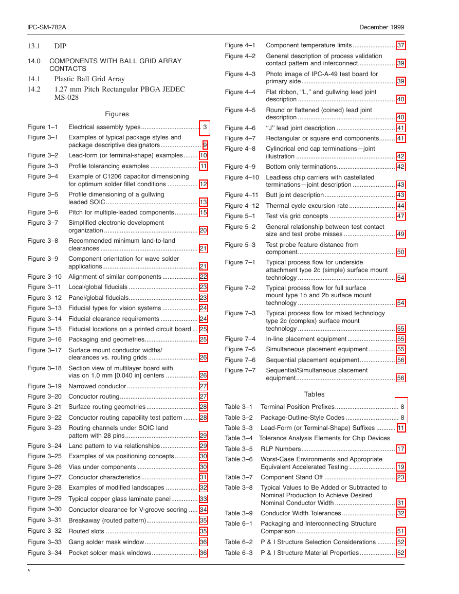
Figures
Figure 3–5
Figure 3–6
Figure 3–7
Figure 1–1
Figure 3–1
Figure 3–2
Figure 3–3
Figure 3–4
Electrical assembly types.................................. 3
Examples of typical package styles and
package descriptive designators....................... 9
Lead-form (or terminal-shape) examples........ 10
Profile tolerancing examples ........................... 11
Example of C1206 capacitor dimensioning
for optimum solder fillet conditions ................. 12
Profile dimensioning of a gullwing
leaded SOIC.................................................... 13
Pitch for multiple-leaded components............. 15
Simplified electronic development
organization ..................................................... 20
Recommended minimum land-to-land
clearances ....................................................... 21
Component orientation for wave solder
applications...................................................... 21
Figure 3–10 Alignment of similar components .................... 22
Figure 3–11
Local/global fiducials ....................................... 23
Figure 3–12 Panel/global fiducials....................................... 23
Figure 3–13 Fiducial types for vision systems .................... 24
Figure 3–14 Fiducial clearance requirements ..................... 24
Figure 3–15 Fiducial locations on a printed circuit board ... 25
Figure 3–16 Packaging and geometries.............................. 25
Figure 3–17 Surface mount conductor widths/
Figure 3–8
Figure 3–9
clearances vs. routing grids ............................ 26
Figure 3–18 Section view of multilayer board with
vias on 1.0 mm [0.040 in] centers .................. 26
Figure 3–19 Narrowed conductor ........................................ 27
Figure 3–20 Conductor routing............................................ 27
Figure 3–21 Surface routing geometries ............................. 28
Figure 3–22 Conductor routing capability test pattern ........ 28
Figure 3–23 Routing channels under SOIC land
pattern with 28 pins......................................... 29
Figure 3–24 Land pattern to via relationships..................... 29
Figure 3–25 Examples of via positioning concepts............. 30
Figure 3–26 Vias under components .................................. 30
Figure 3–27 Conductor characteristics................................ 31
Figure 3–28 Examples of modified landscapes .................. 32
Figure 3–29 Typical copper glass laminate panel............... 33
Figure 3–30 Conductor clearance for V-groove scoring ..... 34
Figure 3–31 Breakaway (routed pattern)............................. 35
Figure 3–32 Routed slots .................................................... 35
Figure 3–33 Gang solder mask window.............................. 36
Figure 3–34 Pocket solder mask windows.......................... 36
v
December 1999
Figure 4–1
Figure 4–2
Figure 4–3
Figure 4–4
Figure 4–5
Figure 4–6
Figure 4–7
Figure 4–8
Component temperature limits ........................ 37
General description of process validation
contact pattern and interconnect..................... 39
Photo image of IPC-A-49 test board for
primary side..................................................... 39
Flat ribbon, ‘‘L,’’ and gullwing lead joint
description ....................................................... 40
Round or flattened (coined) lead joint
description ....................................................... 40
‘‘J’’ lead joint description ................................. 41
Rectangular or square end components......... 41
Cylindrical end cap terminations—joint
illustration ........................................................ 42
Bottom only terminations................................. 42
Figure 4–9
Figure 4–10 Leadless chip carriers with castellated
Figure 7–1
Figure 5–3
terminations—joint description ........................ 43
Figure 4–11 Butt joint description........................................ 43
Figure 4–12 Thermal cycle excursion rate .......................... 44
Test via grid concepts ..................................... 47
Figure 5–1
General relationship between test contact
Figure 5–2
size and test probe misses ............................. 49
Test probe feature distance from
component....................................................... 50
Typical process flow for underside
attachment type 2c (simple) surface mount
technology ....................................................... 54
Typical process flow for full surface
mount type 1b and 2b surface mount
technology ....................................................... 54
Typical process flow for mixed technology
type 2c (complex) surface mount
technology ....................................................... 55
In-line placement equipment ........................... 55
Simultaneous placement equipment ............... 55
Sequential placement equipment.................... 56
Sequential/Simultaneous placement
equipment........................................................ 56
Figure 7–4
Figure 7–5
Figure 7–6
Figure 7–7
Figure 7–2
Figure 7–3
Tables
Table 3–1
Terminal Position Prefixes.................................... 8
Table 3–2 Package-Outline-Style Codes .............................. 8
Table 3–3
Lead-Form (or Terminal-Shape) Suffixes ........... 11
Table 3–4 Tolerance Analysis Elements for Chip Devices
Table 3–5 RLP Numbers..................................................... 17
Table 3–6 Worst-Case Environments and Appropriate
Equivalent Accelerated Testing .......................... 19
Table 3–7 Component Stand Off ........................................ 23
Table 3–8
Typical Values to Be Added or Subtracted to
Nominal Production to Achieve Desired
Nominal Conductor Width .................................. 31
Table 3–9 Conductor Width Tolerances .............................. 32
Table 6–1 Packaging and Interconnecting Structure
Comparison ........................................................ 51
Table 6–2 P & I Structure Selection Considerations .......... 52
Table 6–3 P & I Structure Material Properties .................... 52
�
December 1999
IPC-SM-782A
This Page Intentionally Left Blank
vi
�



 2023年江西萍乡中考道德与法治真题及答案.doc
 2012年重庆南川中考生物真题及答案.doc
 2013年江西师范大学地理学综合及文艺理论基础考研真题.doc
 2020年四川甘孜小升初语文真题及答案I卷.doc
 2020年注册岩土工程师专业基础考试真题及答案.doc
 2023-2024学年福建省厦门市九年级上学期数学月考试题及答案.doc
 2021-2022学年辽宁省沈阳市大东区九年级上学期语文期末试题及答案.doc
 2022-2023学年北京东城区初三第一学期物理期末试卷及答案.doc
 2018上半年江西教师资格初中地理学科知识与教学能力真题及答案.doc
 2012年河北国家公务员申论考试真题及答案-省级.doc
 2020-2021学年江苏省扬州市江都区邵樊片九年级上学期数学第一次质量检测试题及答案.doc
 2022下半年黑龙江教师资格证中学综合素质真题及答案.doc