2015.11.02
SCFIFO and DCFIFO IP Cores User Guide
UG-MFNALT_FIFO
Subscribe
Send Feedback
Altera provides FIFO functions through the parameterizable single-clock FIFO (SCFIFO) and dual-clock
FIFO (DCFIFO) IP cores. The FIFO functions are mostly applied in data buffering applications that
comply with the first-in-first-out data flow in synchronous or asynchronous clock domains.
The specific names of the IP cores are as follows:
• SCFIFO: single-clock FIFO
• DCFIFO: dual-clock FIFO (supports same port widths for input and output data)
• DCFIFO_MIXED_WIDTHS: dual-clock FIFO (supports different port widths for input and output
data)
Note: The term “DCFIFO” refers to both the DCFIFO and DCFIFO_MIXED_WIDTHS IP cores, unless
specified.
Related Information
•
Introduction to Altera IP Cores
Provides general information about all Altera IP cores, including parameterizing, generating,
upgrading, and simulating IP.
• Creating Version-Independent IP and Qsys Simulation Scripts
Create simulation scripts that do not require manual updates for software or IP version upgrades.
• Project Management Best Practices
Guidelines for efficient management and portability of your project and IP files.
Configuration Methods
You can configure and build the FIFO IP cores with the following methods:
Table 1: Configuration Methods
Method
Using the FIFO parameter editor.
Description
Altera recommends using this method to build your
FIFO IP cores. It is an efficient way to configure and
build the FIFO IP cores. The FIFO parameter editor
provides options that you can easily use to
configure the FIFO IP cores.
© 2015 Altera Corporation. All rights reserved. ALTERA, ARRIA, CYCLONE, ENPIRION, MAX, MEGACORE, NIOS, QUARTUS and STRATIX words and logos are
trademarks of Altera Corporation and registered in the U.S. Patent and Trademark Office and in other countries. All other words and logos identified as
trademarks or service marks are the property of their respective holders as described at www.altera.com/common/legal.html. Altera warrants performance
of its semiconductor products to current specifications in accordance with Altera's standard warranty, but reserves the right to make changes to any
products and services at any time without notice. Altera assumes no responsibility or liability arising out of the application or use of any information,
product, or service described herein except as expressly agreed to in writing by Altera. Altera customers are advised to obtain the latest version of device
specifications before relying on any published information and before placing orders for products or services.
ISO
9001:2008
Registered
www.altera.com
101 Innovation Drive, San Jose, CA 95134
�
2
Specifications
UG-MFNALT_FIFO
2015.11.02
Method
Description
Manually instantiating the FIFO IP cores.
Use this method only if you are an expert user. This
method requires that you know the detailed specifi‐
cations of the IP cores. You must ensure that the
input and output ports used, and the parameter
values assigned are valid for the FIFO IP cores you
instantiate for your target device.
Related Information
Introduction to Altera IP Cores
Provides general information about the Quartus® Prime Parameter Editor
Specifications
Verilog HDL Prototype
You can locate the Verilog HDL prototype in the Verilog Design File (.v) altera_mf.v in the \eda\sim_lib directory.
VHDL Component Declaration
The VHDL component declaration is located in the \libraries\vhdl\
altera_mf\altera_mf_components.vhd
VHDL LIBRARY-USE Declaration
The VHDL LIBRARY-USE declaration is not required if you use the VHDL Component Declaration.
LIBRARY altera_mf;
USE altera_mf_altera_mf_components.all;
SCFIFO and DCFIFO Signals
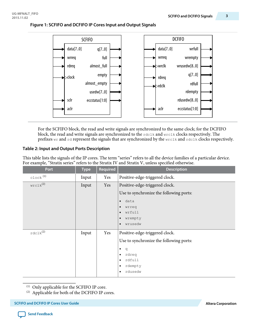
This section provides diagrams of the SCFIFO and DCFIFO blocks to help in visualizing their input and
output ports. This section also describes each port in detail to help in understanding their usages,
functionality, or any restrictions. For better illustrations, some descriptions might refer you to a specific
section in this user guide.
Altera Corporation
SCFIFO and DCFIFO IP Cores User Guide
Send Feedback
�
UG-MFNALT_FIFO
2015.11.02
SCFIFO and DCFIFO Signals
3
Figure 1: SCFIFO and DCFIFO IP Cores Input and Output Signals
SCFIFO
q[7..0]
full
almost_full
empty
almost_empty
usedw[7..0]
eccstatus[1:0]
data[7..0]
wrreq
rdreq
clock
sclr
aclr
DCFIFO
data[7..0]
wrreq
wrclk
rdreq
rdclk
aclr
wrfull
wrempty
wrusedw[8..0]
q[7..0]
rdfull
rdempty
rdusedw[8..0]
eccstatus[1:0]
For the SCFIFO block, the read and write signals are synchronized to the same clock; for the DCFIFO
block, the read and write signals are synchronized to the rdclk and wrclk clocks respectively. The
prefixes wr and rd represent the signals that are synchronized by the wrclk and rdclk clocks respectively.
Table 2: Input and Output Ports Description
This table lists the signals of the IP cores. The term “series” refers to all the device families of a particular device.
For example, “Stratix series” refers to the Stratix IV and Stratix V, unless specified otherwise.
Port
clock (1)
wrclk(2)
Type
Input
Input
Required
Yes
Yes
rdclk(2)
Input
Yes
Description
Positive-edge-triggered clock.
Positive-edge-triggered clock.
Use to synchronize the following ports:
• data
• wrreq
• wrfull
• wrempty
• wrusedw
Positive-edge-triggered clock.
Use to synchronize the following ports:
• q
• rdreq
• rdfull
• rdempty
• rdusedw
(1) Only applicable for the SCFIFO IP core.
(2) Applicable for both of the DCFIFO IP cores.
SCFIFO and DCFIFO IP Cores User Guide
Send Feedback
Altera Corporation
�
4
SCFIFO and DCFIFO Signals
Port
data (3)
Type
Input
Required
Yes
wrreq(3)
Input
Yes
rdreq(3)
Input
Yes
sclr(1)
aclr(3)
Input
No
UG-MFNALT_FIFO
2015.11.02
Description
Holds the data to be written in the FIFO IP core when the
wrreq signal is asserted. If you manually instantiate the
FIFO IP core, ensure the port width is equal to the lpm_
width parameter.
Assert this signal to request for a write operation.
Ensure that the following conditions are met:
• Do not assert the wrreq signal when the full (for
SCFIFO) or wrfull (for DCFIFO) port is high. Enable
the overflow protection circuitry or set the overflow_
checking parameter to ON so that the FIFO IP core
can automatically disable the wrreq signal when it is
full.
• The wrreq signal must meet the functional timing
requirement based on the full or wrfull signal.
• Do not assert the wrreq signal during the deassertion
of the aclr signal. Violating this requirement creates a
race condition between the falling edge of the aclr
signal and the rising edge of the write clock if the
wrreq port is set to high. For both the DCFIFO IP
cores that target Stratix and Cyclone series, you have
the option to automatically add a circuit to
synchronize the aclr signal with the wrclk clock, or
set the write_aclr_synch parameter to ON. Use this
option to ensure that the restriction is obeyed.
Assert this signal to request for a read operation. The
rdreq signal acts differently in normal mode and show-
ahead mode.
Ensure that the following conditions are met:
• Do not assert the rdreq signal when the empty (for
SCFIFO) or rdempty (for DCFIFO) port is high.
Enable the underflow protection circuitry or set the
underflow_checking parameter to ON so that the
FIFO IP core can automatically disable the rdreq
signal when it is empty.
• The rdreq signal must meet the functional timing
requirement based on the empty or rdempty signal.
Assert this signal to clear all the output status ports, but
the effect on the q output may vary for different FIFO
configurations.
There are no minimum number of clock cycles for aclr
signals that must remain active.
(3) Applicable for the SCFIFO, DCFIFO, and DCFIFO_MIXED_WIDTH IP cores.
Altera Corporation
SCFIFO and DCFIFO IP Cores User Guide
Send Feedback
�
UG-MFNALT_FIFO
2015.11.02
Port
q(3)
Type
Output
Required
Yes
full(1)
wrfull(2)(4)
rdfull(2)(4)
empty(1)
wrempty(2)(4)
rdempty(2)(4)
Output
No
Output
No
almost_full(1)
Output
almost_empty (1)
Output
No
No
SCFIFO and DCFIFO Signals
5
Description
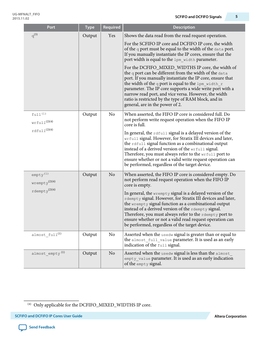
Shows the data read from the read request operation.
For the SCFIFO IP core and DCFIFO IP core, the width
of the q port must be equal to the width of the data port.
If you manually instantiate the IP cores, ensure that the
port width is equal to the lpm_width parameter.
For the DCFIFO_MIXED_WIDTHS IP core, the width of
the q port can be different from the width of the data
port. If you manually instantiate the IP core, ensure that
the width of the q port is equal to the lpm_width_r
parameter. The IP core supports a wide write port with a
narrow read port, and vice versa. However, the width
ratio is restricted by the type of RAM block, and in
general, are in the power of 2.
When asserted, the FIFO IP core is considered full. Do
not perform write request operation when the FIFO IP
core is full.
In general, the rdfull signal is a delayed version of the
wrfull signal. However, for Stratix III devices and later,
the rdfull signal function as a combinational output
instead of a derived version of the wrfull signal.
Therefore, you must always refer to the wrfull port to
ensure whether or not a valid write request operation can
be performed, regardless of the target device.
When asserted, the FIFO IP core is considered empty. Do
not perform read request operation when the FIFO IP
core is empty.
In general, the wrempty signal is a delayed version of the
rdempty signal. However, for Stratix III devices and later,
the wrempty signal function as a combinational output
instead of a derived version of the rdempty signal.
Therefore, you must always refer to the rdempty port to
ensure whether or not a valid read request operation can
be performed, regardless of the target device.
Asserted when the usedw signal is greater than or equal to
the almost_full_value parameter. It is used as an early
indication of the full signal.
Asserted when the usedw signal is less than the almost_
empty_value parameter. It is used as an early indication
of the empty signal.
(4) Only applicable for the DCFIFO_MIXED_WIDTHS IP core.
SCFIFO and DCFIFO IP Cores User Guide
Send Feedback
Altera Corporation
�
6
SCFIFO and DCFIFO Signals
Port
usedw(1)
wrusedw(2)(4)
rdusedw(2)(4)
Type
Output
Required
No
eccstatus(5)
Output
No
UG-MFNALT_FIFO
2015.11.02
Description
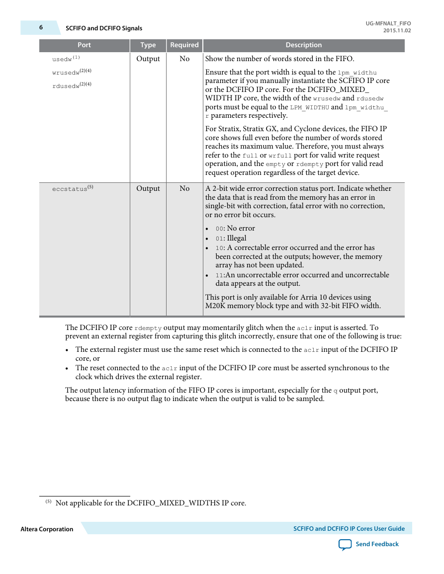
Show the number of words stored in the FIFO.
Ensure that the port width is equal to the lpm_widthu
parameter if you manually instantiate the SCFIFO IP core
or the DCFIFO IP core. For the DCFIFO_MIXED_
WIDTH IP core, the width of the wrusedw and rdusedw
ports must be equal to the LPM_WIDTHU and lpm_widthu_
r parameters respectively.
For Stratix, Stratix GX, and Cyclone devices, the FIFO IP
core shows full even before the number of words stored
reaches its maximum value. Therefore, you must always
refer to the full or wrfull port for valid write request
operation, and the empty or rdempty port for valid read
request operation regardless of the target device.
A 2-bit wide error correction status port. Indicate whether
the data that is read from the memory has an error in
single-bit with correction, fatal error with no correction,
or no error bit occurs.
• 00: No error
• 01: Illegal
• 10: A correctable error occurred and the error has
been corrected at the outputs; however, the memory
array has not been updated.
• 11:An uncorrectable error occurred and uncorrectable
data appears at the output.
This port is only available for Arria 10 devices using
M20K memory block type and with 32-bit FIFO width.
The DCFIFO IP core rdempty output may momentarily glitch when the aclr input is asserted. To
prevent an external register from capturing this glitch incorrectly, ensure that one of the following is true:
• The external register must use the same reset which is connected to the aclr input of the DCFIFO IP
core, or
• The reset connected to the aclr input of the DCFIFO IP core must be asserted synchronous to the
clock which drives the external register.
The output latency information of the FIFO IP cores is important, especially for the q output port,
because there is no output flag to indicate when the output is valid to be sampled.
(5) Not applicable for the DCFIFO_MIXED_WIDTHS IP core.
Altera Corporation
SCFIFO and DCFIFO IP Cores User Guide
Send Feedback
�
UG-MFNALT_FIFO
2015.11.02
SCFIFO and DCFIFO Parameters
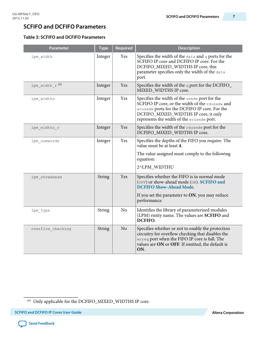
Table 3: SCFIFO and DCFIFO Parameters
Parameter
lpm_width
Type
Integer
Required
Yes
lpm_width_r (6)
lpm_widthu
lpm_widthu_r
lpm_numwords
Integer
Integer
Integer
Integer
Yes
Yes
Yes
Yes
lpm_showahead
String
Yes
lpm_type
overflow_checking
String
String
No
No
SCFIFO and DCFIFO Parameters
7
Description
Specifies the width of the data and q ports for the
SCFIFO IP core and DCFIFO IP core. For the
DCFIFO_MIXED_WIDTHS IP core, this
parameter specifies only the width of the data
port.
Specifies the width of the q port for the DCFIFO_
MIXED_WIDTHS IP core.
Specifies the width of the usedw port for the
SCFIFO IP core, or the width of the rdusedw and
wrusedw ports for the DCFIFO IP core. For the
DCFIFO_MIXED_WIDTHS IP core, it only
represents the width of the wrusedw port.
Specifies the width of the rdusedw port for the
DCFIFO_MIXED_WIDTHS IP core.
Specifies the depths of the FIFO you require. The
value must be at least 4.
The value assigned must comply to the following
equation:
2^LPM_WIDTHU
Specifies whether the FIFO is in normal mode
(OFF) or show-ahead mode (ON). SCFIFO and
DCFIFO Show-Ahead Mode.
If you set the parameter to ON, you may reduce
performance.
Identifies the library of parameterized modules
(LPM) entity name. The values are SCFIFO and
DCFIFO.
Specifies whether or not to enable the protection
circuitry for overflow checking that disables the
wrreq port when the FIFO IP core is full. The
values are ON or OFF. If omitted, the default is
ON.
(6) Only applicable for the DCFIFO_MIXED_WIDTHS IP core.
SCFIFO and DCFIFO IP Cores User Guide
Send Feedback
Altera Corporation
�
8
SCFIFO and DCFIFO Parameters
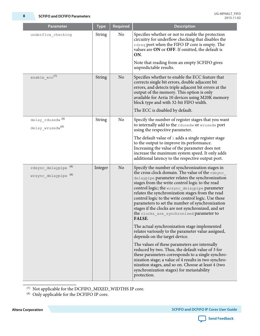
Parameter
underflow_checking
Type
String
Required
No
enable_ecc(7)
String
No
delay_rdusedw (8)
delay_wrusedw(8)
String
No
rdsync_delaypipe (8)
wrsync_delaypipe (8)
Integer
No
UG-MFNALT_FIFO
2015.11.02
Description
Specifies whether or not to enable the protection
circuitry for underflow checking that disables the
rdreq port when the FIFO IP core is empty. The
values are ON or OFF. If omitted, the default is
ON.
Note that reading from an empty SCFIFO gives
unpredictable results.
Specifies whether to enable the ECC feature that
corrects single bit errors, double adjacent bit
errors, and detects triple adjacent bit errors at the
output of the memory. This option is only
available for Arria 10 devices using M20K memory
block type and with 32-bit FIFO width.
The ECC is disabled by default.
Specify the number of register stages that you want
to internally add to the rdusedw or wrusedw port
using the respective parameter.
The default value of 1 adds a single register stage
to the output to improve its performance.
Increasing the value of the parameter does not
increase the maximum system speed. It only adds
additional latency to the respective output port.
Specify the number of synchronization stages in
the cross clock domain. The value of the rdsync_
delaypipe parameter relates the synchronization
stages from the write control logic to the read
control logic; the wrsync_delaypipe parameter
relates the synchronization stages from the read
control logic to the write control logic. Use these
parameters to set the number of synchronization
stages if the clocks are not synchronized, and set
the clocks_are_synchronized parameter to
FALSE.
The actual synchronization stage implemented
relates variously to the parameter value assigned,
depends on the target device.
The values of these parameters are internally
reduced by two. Thus, the default value of 3 for
these parameters corresponds to a single synchro‐
nization stage; a value of 4 results in two synchro‐
nization stages, and so on. Choose at least 4 (two
synchronization stages) for metastability
protection.
(7) Not applicable for the DCFIFO_MIXED_WIDTHS IP core.
(8) Only applicable for the DCFIFO IP core.
Altera Corporation
SCFIFO and DCFIFO IP Cores User Guide
Send Feedback
�




 2023年江西萍乡中考道德与法治真题及答案.doc
 2012年重庆南川中考生物真题及答案.doc
 2013年江西师范大学地理学综合及文艺理论基础考研真题.doc
 2020年四川甘孜小升初语文真题及答案I卷.doc
 2020年注册岩土工程师专业基础考试真题及答案.doc
 2023-2024学年福建省厦门市九年级上学期数学月考试题及答案.doc
 2021-2022学年辽宁省沈阳市大东区九年级上学期语文期末试题及答案.doc
 2022-2023学年北京东城区初三第一学期物理期末试卷及答案.doc
 2018上半年江西教师资格初中地理学科知识与教学能力真题及答案.doc
 2012年河北国家公务员申论考试真题及答案-省级.doc
 2020-2021学年江苏省扬州市江都区邵樊片九年级上学期数学第一次质量检测试题及答案.doc
 2022下半年黑龙江教师资格证中学综合素质真题及答案.doc