logo资料库

STM32L151技术手册.pdf

第1页 / 共132页
第2页 / 共132页
第3页 / 共132页
第4页 / 共132页
第5页 / 共132页
第6页 / 共132页
第7页 / 共132页
第8页 / 共132页
资料共132页,剩余部分请下载后查看
Table 1. Device summary
1 Introduction
2 Description
2.1 Device overview
Table 2. Ultra-low-power STM32L151x6/8/B and STM32L152x6/8/B device features and peripheral counts
2.2 Ultra-low-power device continuum
2.2.1 Performance
2.2.2 Shared peripherals
2.2.3 Common system strategy
2.2.4 Features
3 Functional overview
Figure 1. Ultra-low-power STM32L151x6/8/B and STM32L152x6/8/B block diagram
3.1 Low power modes
Table 3. Functionalities depending on the operating power supply range
Table 4. CPU frequency range depending on dynamic voltage scaling
Table 5. Working mode-dependent functionalities (from Run/active down to standby)
3.2 ARM® Cortex®-M3 core with MPU
3.3 Reset and supply management
3.3.1 Power supply schemes
3.3.2 Power supply supervisor
3.3.3 Voltage regulator
3.3.4 Boot modes
3.4 Clock management
Figure 2. Clock tree
3.5 Low power real-time clock and backup registers
3.6 GPIOs (general-purpose inputs/outputs)
3.7 Memories
3.8 DMA (direct memory access)
3.9 LCD (liquid crystal display)
3.10 ADC (analog-to-digital converter)
3.10.1 Temperature sensor
3.10.2 Internal voltage reference (VREFINT)
3.11 DAC (digital-to-analog converter)
3.12 Ultra-low-power comparators and reference voltage
3.13 Routing interface
3.14 Touch sensing
3.15 Timers and watchdogs
Table 6. Timer feature comparison
3.15.1 General-purpose timers (TIM2, TIM3, TIM4, TIM9, TIM10 and TIM11)
3.15.2 Basic timers (TIM6 and TIM7)
3.15.3 SysTick timer
3.15.4 Independent watchdog (IWDG)
3.15.5 Window watchdog (WWDG)
3.16 Communication interfaces
3.16.1 I²C bus
3.16.2 Universal synchronous/asynchronous receiver transmitter (USART)
3.16.3 Serial peripheral interface (SPI)
3.16.4 Universal serial bus (USB)
3.17 CRC (cyclic redundancy check) calculation unit
3.18 Development support
4 Pin descriptions
Figure 3. STM32L15xVx UFBGA100 ballout
Figure 4. STM32L15xVx LQFP100 pinout
Figure 5. STM32L15xRx TFBGA64 ballout
Figure 6. STM32L15xRx LQFP64 pinout
Figure 7. STM32L15xCx LQFP48 pinout
Figure 8. STM32L15xCx UFQFPN48 pinout
Table 7. Legend/abbreviations used in the pinout table
Table 8. STM32L151x6/8/B and STM32L152x6/8/B pin definitions
Table 9. Alternate function input/output
5 Memory mapping
Figure 9. Memory map
6 Electrical characteristics
6.1 Parameter conditions
6.1.1 Minimum and maximum values
6.1.2 Typical values
6.1.3 Typical curves
6.1.4 Loading capacitor
6.1.5 Pin input voltage
Figure 10. Pin loading conditions
Figure 11. Pin input voltage
6.1.6 Power supply scheme
Figure 12. Power supply scheme
6.1.7 Optional LCD power supply scheme
Figure 13. Optional LCD power supply scheme
6.1.8 Current consumption measurement
Figure 14. Current consumption measurement scheme
6.2 Absolute maximum ratings
Table 10. Voltage characteristics
Table 11. Current characteristics
Table 12. Thermal characteristics
6.3 Operating conditions
6.3.1 General operating conditions
Table 13. General operating conditions
6.3.2 Embedded reset and power control block characteristics
Table 14. Embedded reset and power control block characteristics
6.3.3 Embedded internal reference voltage
Table 15. Embedded internal reference voltage calibration values
Table 16. Embedded internal reference voltage
6.3.4 Supply current characteristics
Table 17. Current consumption in Run mode, code with data processing running from Flash
Table 18. Current consumption in Run mode, code with data processing running from RAM
Table 19. Current consumption in Sleep mode
Table 20. Current consumption in Low power run mode
Table 21. Current consumption in Low power sleep mode
Table 22. Typical and maximum current consumptions in Stop mode
Table 23. Typical and maximum current consumptions in Standby mode
Table 24. Peripheral current consumption
6.3.5 Wakeup time from Low power mode
Table 25. Low-power mode wakeup timings
6.3.6 External clock source characteristics
Table 26. High-speed external user clock characteristics
Figure 15. High-speed external clock source AC timing diagram
Table 27. Low-speed external user clock characteristics
Figure 16. Low-speed external clock source AC timing diagram
Table 28. HSE oscillator characteristics
Figure 17. HSE oscillator circuit diagram
Table 29. LSE oscillator characteristics (fLSE = 32.768 kHz)
Figure 18. Typical application with a 32.768 kHz crystal
6.3.7 Internal clock source characteristics
Table 30. HSI oscillator characteristics
Table 31. LSI oscillator characteristics
Table 32. MSI oscillator characteristics
6.3.8 PLL characteristics
Table 33. PLL characteristics
6.3.9 Memory characteristics
Table 34. RAM and hardware registers
Table 35. Flash memory and data EEPROM characteristics
Table 36. Flash memory, data EEPROM endurance and data retention
6.3.10 EMC characteristics
Table 37. EMS characteristics
Table 38. EMI characteristics
6.3.11 Electrical sensitivity characteristics
Table 39. ESD absolute maximum ratings
Table 40. Electrical sensitivities
6.3.12 I/O current injection characteristics
Table 41. I/O current injection susceptibility
6.3.13 I/O port characteristics
Table 42. I/O static characteristics
Table 43. Output voltage characteristics
Table 44. I/O AC characteristics
Figure 19. I/O AC characteristics definition
6.3.14 NRST pin characteristics
Table 45. NRST pin characteristics
Figure 20. Recommended NRST pin protection
6.3.15 TIM timer characteristics
Table 46. TIMx characteristics
6.3.16 Communication interfaces
Table 47. I2C characteristics
Figure 21. I2C bus AC waveforms and measurement circuit
Table 48. SCL frequency (fPCLK1= 32 MHz, VDD = VDD_I2C = 3.3 V)
Table 49. SPI characteristics
Figure 22. SPI timing diagram - slave mode and CPHA = 0
Figure 23. SPI timing diagram - slave mode and CPHA = 1(1)
Figure 24. SPI timing diagram - master mode(1)
Table 50. USB startup time
Table 51. USB DC electrical characteristics
Figure 25. USB timings: definition of data signal rise and fall time
Table 52. USB: full speed electrical characteristics
6.3.17 12-bit ADC characteristics
Table 53. ADC clock frequency
Table 54. ADC characteristics
Table 55. ADC accuracy
Figure 26. ADC accuracy characteristics
Figure 27. Typical connection diagram using the ADC
Figure 28. Maximum dynamic current consumption on VREF+ supply pin during ADC conversion
Table 56. Maximum source impedance RAIN max
Figure 29. Power supply and reference decoupling (VREF+ not connected to VDDA)
Figure 30. Power supply and reference decoupling (VREF+ connected to VDDA)
6.3.18 DAC electrical specifications
Table 57. DAC characteristics
Figure 31. 12-bit buffered /non-buffered DAC
6.3.19 Temperature sensor characteristics
Table 58. Temperature sensor calibration values
Table 59. Temperature sensor characteristics
6.3.20 Comparator
Table 60. Comparator 1 characteristics
Table 61. Comparator 2 characteristics
6.3.21 LCD controller (STM32L152xx only)
Table 62. LCD controller characteristics
7 Package characteristics
7.1 Package mechanical data
Figure 32. LQFP100 14 x 14 mm, 100-pin low-profile quad flat package outline
Table 63. LQPF100 14 x 14 mm, 100-pin low-profile quad flat package mechanical data
Figure 33. LQFP100 recommended footprint
Figure 34. LQFP100 marking example (package top view)
Figure 35. LQFP64 10 x 10 mm, 64-pin low-profile quad flat package outline
Table 64. LQFP64 10 x 10 mm 64-pin low-profile quad flat package mechanical data
Figure 36. LQFP64 recommended footprint
Figure 37. LQFP64 marking example (package top view)
Figure 38. LQFP48 7 x 7 mm, 48-pin low-profile quad flat package outline
Table 65. LQFP48 7 x 7 mm, 48-pin low-profile quad flat package mechanical data
Figure 39. LQFP48 recommended footprint
Figure 40. LQFP48 marking example (package top view)
Figure 41. UFQFPN48 7 x 7 mm 0.5 mm pitch, ultra thin fine-pitch quad flat no-lead package outline
Table 66. UFQFPN48 7 x 7 mm, 0.5 mm pitch, ultra thin fine-pitch quad flat no-lead package mechanical data
Figure 42. UFQFPN48 recommended footprint
Figure 43. UFQFPN48 marking example (package top view)
Figure 44. UFBGA100 7 x 7 x 0.6 mm 0.5 mm pitch, ultra thin fine-pitch ball grid array package outline
Table 67. UFBGA100 7 x 7 x 0.6 mm 0.5 mm pitch, ultra thin fine-pitch ball grid array package mechanical data
Figure 45. UFBGA100 marking example (package top view)
Figure 46. TFBGA64 - 5.0x5.0x1.2 mm, 0.5 mm pitch, thin fine-pitch ball grid array package outline
Table 68. TFBGA64 5.0x5.0x1.2 mm, 0.5 mm pitch thin fine-pitch ball grid array package mechanical data
Figure 47. TFBGA64 marking example (package top view)
Figure 48. Recommended PCB design rules for pads (0.5 mm pitch BGA)
7.2 Thermal characteristics
Table 69. Thermal characteristics
Figure 49. Thermal resistance
7.2.1 Reference document
8 Part numbering
Table 70. Ordering information scheme
9 Revision history
Table 71. Document revision history
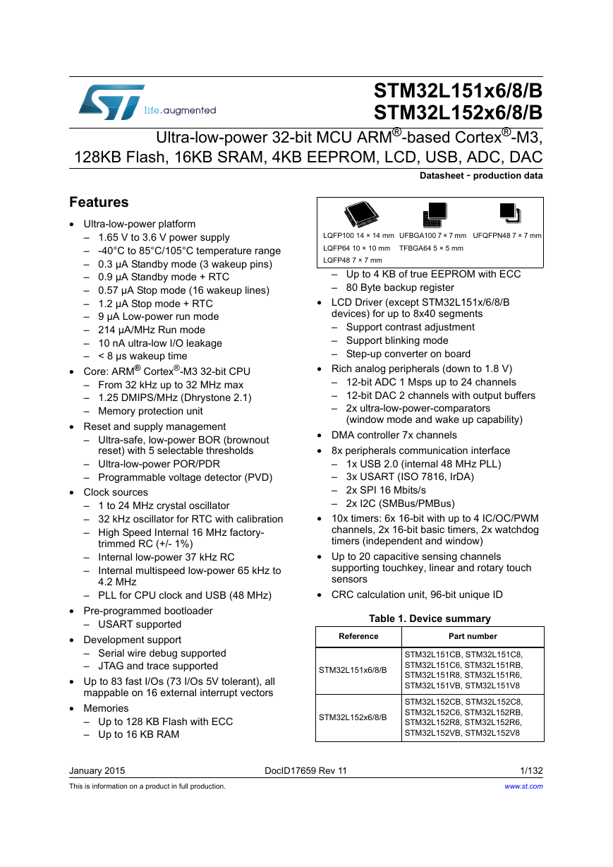
STM32L151x6/8/B STM32L152x6/8/B Ultra-low-power 32-bit MCU ARM®-based Cortex®-M3, 128KB Flash, 16KB SRAM, 4KB EEPROM, LCD, USB, ADC, DAC Datasheet - production data Features • Ultra-low-power platform – 1.65 V to 3.6 V power supply – -40°C to 85°C/105°C temperature range – 0.3 µA Standby mode (3 wakeup pins) – 0.9 µA Standby mode + RTC – 0.57 µA Stop mode (16 wakeup lines) – 1.2 µA Stop mode + RTC – 9 µA Low-power run mode – 214 µA/MHz Run mode – 10 nA ultra-low I/O leakage – < 8 µs wakeup time • Core: ARM® Cortex®-M3 32-bit CPU – From 32 kHz up to 32 MHz max – 1.25 DMIPS/MHz (Dhrystone 2.1) – Memory protection unit • Reset and supply management – Ultra-safe, low-power BOR (brownout reset) with 5 selectable thresholds – Ultra-low-power POR/PDR – Programmable voltage detector (PVD) • Clock sources – 1 to 24 MHz crystal oscillator – 32 kHz oscillator for RTC with calibration – High Speed Internal 16 MHz factory- trimmed RC (+/- 1%) – Internal low-power 37 kHz RC – Internal multispeed low-power 65 kHz to 4.2 MHz – PLL for CPU clock and USB (48 MHz) • Pre-programmed bootloader – USART supported • Development support – Serial wire debug supported – JTAG and trace supported • Up to 83 fast I/Os (73 I/Os 5V tolerant), all mappable on 16 external interrupt vectors • Memories – Up to 128 KB Flash with ECC – Up to 16 KB RAM LQFP100 14 × 14 mm LQFP64 10 × 10 mm LQFP48 7 × 7 mm UFBGA100 7 × 7 mm TFBGA64 5 × 5 mm UFQFPN48 7 × 7 mm – Up to 4 KB of true EEPROM with ECC – 80 Byte backup register • LCD Driver (except STM32L151x/6/8/B devices) for up to 8x40 segments – Support contrast adjustment – Support blinking mode – Step-up converter on board • Rich analog peripherals (down to 1.8 V) – 12-bit ADC 1 Msps up to 24 channels – 12-bit DAC 2 channels with output buffers – 2x ultra-low-power-comparators (window mode and wake up capability) • DMA controller 7x channels • 8x peripherals communication interface – 1x USB 2.0 (internal 48 MHz PLL) – 3x USART (ISO 7816, IrDA) – 2x SPI 16 Mbits/s – 2x I2C (SMBus/PMBus) • 10x timers: 6x 16-bit with up to 4 IC/OC/PWM channels, 2x 16-bit basic timers, 2x watchdog timers (independent and window) • Up to 20 capacitive sensing channels supporting touchkey, linear and rotary touch sensors • CRC calculation unit, 96-bit unique ID Table 1. Device summary Part number Reference STM32L151x6/8/B STM32L152x6/8/B STM32L151CB, STM32L151C8, STM32L151C6, STM32L151RB, STM32L151R8, STM32L151R6, STM32L151VB, STM32L151V8 STM32L152CB, STM32L152C8, STM32L152C6, STM32L152RB, STM32L152R8, STM32L152R6, STM32L152VB, STM32L152V8 January 2015 This is information on a product in full production. DocID17659 Rev 11 1/132 www.st.com
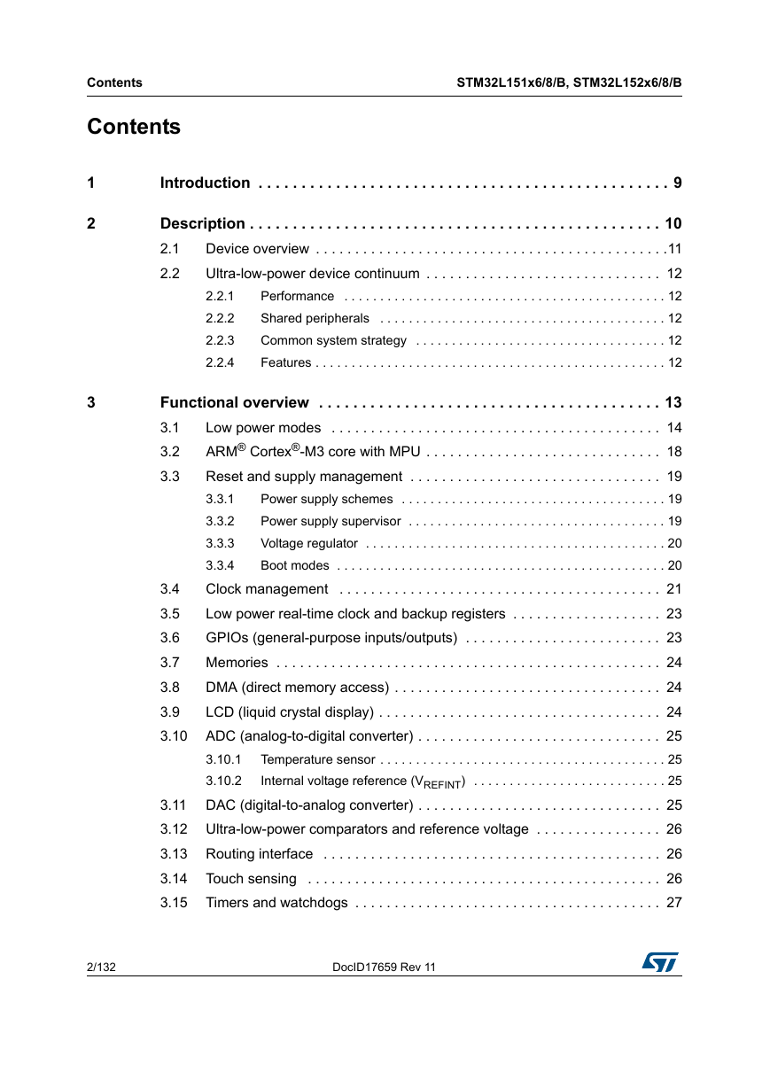
Contents Contents STM32L151x6/8/B, STM32L152x6/8/B 1 2 3 Introduction . . . . . . . . . . . . . . . . . . . . . . . . . . . . . . . . . . . . . . . . . . . . . . . . 9 Description . . . . . . . . . . . . . . . . . . . . . . . . . . . . . . . . . . . . . . . . . . . . . . . . 10 Device overview . . . . . . . . . . . . . . . . . . . . . . . . . . . . . . . . . . . . . . . . . . . . .11 2.1 Ultra-low-power device continuum . . . . . . . . . . . . . . . . . . . . . . . . . . . . . . 12 2.2 2.2.1 Performance . . . . . . . . . . . . . . . . . . . . . . . . . . . . . . . . . . . . . . . . . . . . . 12 Shared peripherals . . . . . . . . . . . . . . . . . . . . . . . . . . . . . . . . . . . . . . . . 12 2.2.2 Common system strategy . . . . . . . . . . . . . . . . . . . . . . . . . . . . . . . . . . . 12 2.2.3 2.2.4 Features . . . . . . . . . . . . . . . . . . . . . . . . . . . . . . . . . . . . . . . . . . . . . . . . . 12 Functional overview . . . . . . . . . . . . . . . . . . . . . . . . . . . . . . . . . . . . . . . . 13 3.1 Low power modes . . . . . . . . . . . . . . . . . . . . . . . . . . . . . . . . . . . . . . . . . . 14 ARM® Cortex®-M3 core with MPU . . . . . . . . . . . . . . . . . . . . . . . . . . . . . . 18 3.2 3.3 Reset and supply management . . . . . . . . . . . . . . . . . . . . . . . . . . . . . . . . 19 Power supply schemes . . . . . . . . . . . . . . . . . . . . . . . . . . . . . . . . . . . . . 19 3.3.1 Power supply supervisor . . . . . . . . . . . . . . . . . . . . . . . . . . . . . . . . . . . . 19 3.3.2 3.3.3 Voltage regulator . . . . . . . . . . . . . . . . . . . . . . . . . . . . . . . . . . . . . . . . . . 20 3.3.4 Boot modes . . . . . . . . . . . . . . . . . . . . . . . . . . . . . . . . . . . . . . . . . . . . . . 20 Clock management . . . . . . . . . . . . . . . . . . . . . . . . . . . . . . . . . . . . . . . . . 21 3.4 Low power real-time clock and backup registers . . . . . . . . . . . . . . . . . . . 23 3.5 GPIOs (general-purpose inputs/outputs) . . . . . . . . . . . . . . . . . . . . . . . . . 23 3.6 Memories . . . . . . . . . . . . . . . . . . . . . . . . . . . . . . . . . . . . . . . . . . . . . . . . . 24 3.7 DMA (direct memory access) . . . . . . . . . . . . . . . . . . . . . . . . . . . . . . . . . . 24 3.8 3.9 LCD (liquid crystal display) . . . . . . . . . . . . . . . . . . . . . . . . . . . . . . . . . . . . 24 3.10 ADC (analog-to-digital converter) . . . . . . . . . . . . . . . . . . . . . . . . . . . . . . . 25 Temperature sensor . . . . . . . . . . . . . . . . . . . . . . . . . . . . . . . . . . . . . . . . 25 Internal voltage reference (VREFINT) . . . . . . . . . . . . . . . . . . . . . . . . . . . 25 3.11 DAC (digital-to-analog converter) . . . . . . . . . . . . . . . . . . . . . . . . . . . . . . . 25 3.12 Ultra-low-power comparators and reference voltage . . . . . . . . . . . . . . . . 26 3.13 Routing interface . . . . . . . . . . . . . . . . . . . . . . . . . . . . . . . . . . . . . . . . . . . 26 3.14 Touch sensing . . . . . . . . . . . . . . . . . . . . . . . . . . . . . . . . . . . . . . . . . . . . . 26 Timers and watchdogs . . . . . . . . . . . . . . . . . . . . . . . . . . . . . . . . . . . . . . . 27 3.15 3.10.1 3.10.2 2/132 DocID17659 Rev 11
STM32L151x6/8/B, STM32L152x6/8/B Contents 4 5 6 3.15.1 General-purpose timers (TIM2, TIM3, TIM4, TIM9, TIM10 and TIM11) . 28 Basic timers (TIM6 and TIM7) . . . . . . . . . . . . . . . . . . . . . . . . . . . . . . . . 28 3.15.2 3.15.3 SysTick timer . . . . . . . . . . . . . . . . . . . . . . . . . . . . . . . . . . . . . . . . . . . . . 28 3.15.4 Independent watchdog (IWDG) . . . . . . . . . . . . . . . . . . . . . . . . . . . . . . . 28 3.15.5 Window watchdog (WWDG) . . . . . . . . . . . . . . . . . . . . . . . . . . . . . . . . . 29 3.16 Communication interfaces . . . . . . . . . . . . . . . . . . . . . . . . . . . . . . . . . . . . 29 I²C bus . . . . . . . . . . . . . . . . . . . . . . . . . . . . . . . . . . . . . . . . . . . . . . . . . . 29 Universal synchronous/asynchronous receiver transmitter (USART) . . 29 Serial peripheral interface (SPI) . . . . . . . . . . . . . . . . . . . . . . . . . . . . . . . 29 Universal serial bus (USB) . . . . . . . . . . . . . . . . . . . . . . . . . . . . . . . . . . . 29 3.17 CRC (cyclic redundancy check) calculation unit . . . . . . . . . . . . . . . . . . . 30 3.18 Development support . . . . . . . . . . . . . . . . . . . . . . . . . . . . . . . . . . . . . . . . 30 3.16.1 3.16.2 3.16.3 3.16.4 Pin descriptions . . . . . . . . . . . . . . . . . . . . . . . . . . . . . . . . . . . . . . . . . . . 31 Memory mapping . . . . . . . . . . . . . . . . . . . . . . . . . . . . . . . . . . . . . . . . . . . 48 Electrical characteristics . . . . . . . . . . . . . . . . . . . . . . . . . . . . . . . . . . . . 49 Parameter conditions . . . . . . . . . . . . . . . . . . . . . . . . . . . . . . . . . . . . . . . . 49 6.1 6.1.1 Minimum and maximum values . . . . . . . . . . . . . . . . . . . . . . . . . . . . . . . 49 Typical values . . . . . . . . . . . . . . . . . . . . . . . . . . . . . . . . . . . . . . . . . . . . 49 6.1.2 Typical curves . . . . . . . . . . . . . . . . . . . . . . . . . . . . . . . . . . . . . . . . . . . . 49 6.1.3 6.1.4 Loading capacitor . . . . . . . . . . . . . . . . . . . . . . . . . . . . . . . . . . . . . . . . . 49 Pin input voltage . . . . . . . . . . . . . . . . . . . . . . . . . . . . . . . . . . . . . . . . . . 49 6.1.5 Power supply scheme . . . . . . . . . . . . . . . . . . . . . . . . . . . . . . . . . . . . . . 50 6.1.6 6.1.7 Optional LCD power supply scheme . . . . . . . . . . . . . . . . . . . . . . . . . . . 51 6.1.8 Current consumption measurement . . . . . . . . . . . . . . . . . . . . . . . . . . . 51 Absolute maximum ratings . . . . . . . . . . . . . . . . . . . . . . . . . . . . . . . . . . . . 52 Operating conditions . . . . . . . . . . . . . . . . . . . . . . . . . . . . . . . . . . . . . . . . 53 General operating conditions . . . . . . . . . . . . . . . . . . . . . . . . . . . . . . . . . 53 6.3.1 Embedded reset and power control block characteristics . . . . . . . . . . . 54 6.3.2 6.3.3 Embedded internal reference voltage . . . . . . . . . . . . . . . . . . . . . . . . . . 56 Supply current characteristics . . . . . . . . . . . . . . . . . . . . . . . . . . . . . . . . 57 6.3.4 Wakeup time from Low power mode . . . . . . . . . . . . . . . . . . . . . . . . . . . 69 6.3.5 6.3.6 External clock source characteristics . . . . . . . . . . . . . . . . . . . . . . . . . . . 70 Internal clock source characteristics . . . . . . . . . . . . . . . . . . . . . . . . . . . 75 6.3.7 6.3.8 PLL characteristics . . . . . . . . . . . . . . . . . . . . . . . . . . . . . . . . . . . . . . . . 77 6.2 6.3 DocID17659 Rev 11 3/132 4
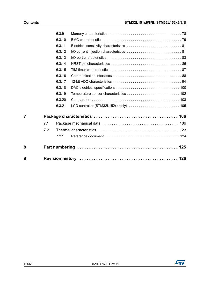
Contents STM32L151x6/8/B, STM32L152x6/8/B 6.3.9 6.3.10 6.3.11 6.3.12 6.3.13 6.3.14 6.3.15 6.3.16 6.3.17 6.3.18 6.3.19 6.3.20 6.3.21 Memory characteristics . . . . . . . . . . . . . . . . . . . . . . . . . . . . . . . . . . . . . 78 EMC characteristics . . . . . . . . . . . . . . . . . . . . . . . . . . . . . . . . . . . . . . . . 79 Electrical sensitivity characteristics . . . . . . . . . . . . . . . . . . . . . . . . . . . . 81 I/O current injection characteristics . . . . . . . . . . . . . . . . . . . . . . . . . . . . 81 I/O port characteristics . . . . . . . . . . . . . . . . . . . . . . . . . . . . . . . . . . . . . . 83 NRST pin characteristics . . . . . . . . . . . . . . . . . . . . . . . . . . . . . . . . . . . . 86 TIM timer characteristics . . . . . . . . . . . . . . . . . . . . . . . . . . . . . . . . . . . . 87 Communication interfaces . . . . . . . . . . . . . . . . . . . . . . . . . . . . . . . . . . . 88 12-bit ADC characteristics . . . . . . . . . . . . . . . . . . . . . . . . . . . . . . . . . . . 94 DAC electrical specifications . . . . . . . . . . . . . . . . . . . . . . . . . . . . . . . . 100 Temperature sensor characteristics . . . . . . . . . . . . . . . . . . . . . . . . . . . 102 Comparator . . . . . . . . . . . . . . . . . . . . . . . . . . . . . . . . . . . . . . . . . . . . . 103 LCD controller (STM32L152xx only) . . . . . . . . . . . . . . . . . . . . . . . . . . 105 7 8 9 Package characteristics . . . . . . . . . . . . . . . . . . . . . . . . . . . . . . . . . . . . 106 Package mechanical data . . . . . . . . . . . . . . . . . . . . . . . . . . . . . . . . . . . 106 7.1 7.2 Thermal characteristics . . . . . . . . . . . . . . . . . . . . . . . . . . . . . . . . . . . . . 123 Reference document . . . . . . . . . . . . . . . . . . . . . . . . . . . . . . . . . . . . . . 124 7.2.1 Part numbering . . . . . . . . . . . . . . . . . . . . . . . . . . . . . . . . . . . . . . . . . . . 125 Revision history . . . . . . . . . . . . . . . . . . . . . . . . . . . . . . . . . . . . . . . . . . 126 4/132 DocID17659 Rev 11
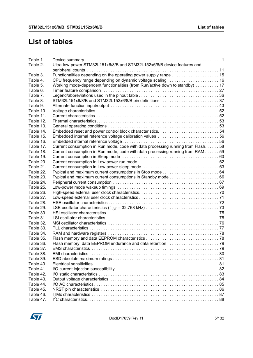
STM32L151x6/8/B, STM32L152x6/8/B List of tables List of tables Table 1. Table 2. Device summary . . . . . . . . . . . . . . . . . . . . . . . . . . . . . . . . . . . . . . . . . . . . . . . . . . . . . . . . . . 1 Ultra-low-power STM32L151x6/8/B and STM32L152x6/8/B device features and peripheral counts . . . . . . . . . . . . . . . . . . . . . . . . . . . . . . . . . . . . . . . . . . . . . . . . . . . . . . . . 11 Table 3. Functionalities depending on the operating power supply range . . . . . . . . . . . . . . . . . . . . 15 Table 4. CPU frequency range depending on dynamic voltage scaling . . . . . . . . . . . . . . . . . . . . . . 16 Table 5. Working mode-dependent functionalities (from Run/active down to standby) . . . . . . . . . . 17 Table 6. Timer feature comparison. . . . . . . . . . . . . . . . . . . . . . . . . . . . . . . . . . . . . . . . . . . . . . . . . . 27 Table 7. Legend/abbreviations used in the pinout table . . . . . . . . . . . . . . . . . . . . . . . . . . . . . . . . . . 36 Table 8. STM32L151x6/8/B and STM32L152x6/8/B pin definitions . . . . . . . . . . . . . . . . . . . . . . . . . 37 Table 9. Alternate function input/output . . . . . . . . . . . . . . . . . . . . . . . . . . . . . . . . . . . . . . . . . . . . . . 43 Table 10. Voltage characteristics . . . . . . . . . . . . . . . . . . . . . . . . . . . . . . . . . . . . . . . . . . . . . . . . . . . . 52 Table 11. Current characteristics . . . . . . . . . . . . . . . . . . . . . . . . . . . . . . . . . . . . . . . . . . . . . . . . . . . . 52 Table 12. Thermal characteristics. . . . . . . . . . . . . . . . . . . . . . . . . . . . . . . . . . . . . . . . . . . . . . . . . . . . 53 Table 13. General operating conditions . . . . . . . . . . . . . . . . . . . . . . . . . . . . . . . . . . . . . . . . . . . . . . . 53 Embedded reset and power control block characteristics. . . . . . . . . . . . . . . . . . . . . . . . . . 54 Table 14. Embedded internal reference voltage calibration values . . . . . . . . . . . . . . . . . . . . . . . . . . 56 Table 15. Table 16. Embedded internal reference voltage. . . . . . . . . . . . . . . . . . . . . . . . . . . . . . . . . . . . . . . . . 56 Current consumption in Run mode, code with data processing running from Flash. . . . . . 58 Table 17. Current consumption in Run mode, code with data processing running from RAM . . . . . . 59 Table 18. Current consumption in Sleep mode . . . . . . . . . . . . . . . . . . . . . . . . . . . . . . . . . . . . . . . . . 60 Table 19. Table 20. Current consumption in Low power run mode . . . . . . . . . . . . . . . . . . . . . . . . . . . . . . . . . . 62 Current consumption in Low power sleep mode. . . . . . . . . . . . . . . . . . . . . . . . . . . . . . . . . 63 Table 21. Typical and maximum current consumptions in Stop mode . . . . . . . . . . . . . . . . . . . . . . . . 64 Table 22. Typical and maximum current consumptions in Standby mode . . . . . . . . . . . . . . . . . . . . . 66 Table 23. Table 24. Peripheral current consumption . . . . . . . . . . . . . . . . . . . . . . . . . . . . . . . . . . . . . . . . . . . . . 67 Low-power mode wakeup timings . . . . . . . . . . . . . . . . . . . . . . . . . . . . . . . . . . . . . . . . . . . 69 Table 25. High-speed external user clock characteristics. . . . . . . . . . . . . . . . . . . . . . . . . . . . . . . . . . 70 Table 26. Low-speed external user clock characteristics . . . . . . . . . . . . . . . . . . . . . . . . . . . . . . . . . . 71 Table 27. Table 28. HSE oscillator characteristics . . . . . . . . . . . . . . . . . . . . . . . . . . . . . . . . . . . . . . . . . . . . . . . 72 LSE oscillator characteristics (fLSE = 32.768 kHz) . . . . . . . . . . . . . . . . . . . . . . . . . . . . . . . 73 Table 29. HSI oscillator characteristics. . . . . . . . . . . . . . . . . . . . . . . . . . . . . . . . . . . . . . . . . . . . . . . . 75 Table 30. Table 31. LSI oscillator characteristics . . . . . . . . . . . . . . . . . . . . . . . . . . . . . . . . . . . . . . . . . . . . . . . . 75 Table 32. MSI oscillator characteristics . . . . . . . . . . . . . . . . . . . . . . . . . . . . . . . . . . . . . . . . . . . . . . . 76 PLL characteristics . . . . . . . . . . . . . . . . . . . . . . . . . . . . . . . . . . . . . . . . . . . . . . . . . . . . . . . 77 Table 33. RAM and hardware registers . . . . . . . . . . . . . . . . . . . . . . . . . . . . . . . . . . . . . . . . . . . . . . . 78 Table 34. Flash memory and data EEPROM characteristics . . . . . . . . . . . . . . . . . . . . . . . . . . . . . . . 78 Table 35. Flash memory, data EEPROM endurance and data retention . . . . . . . . . . . . . . . . . . . . . . 79 Table 36. Table 37. EMS characteristics . . . . . . . . . . . . . . . . . . . . . . . . . . . . . . . . . . . . . . . . . . . . . . . . . . . . . . 79 EMI characteristics . . . . . . . . . . . . . . . . . . . . . . . . . . . . . . . . . . . . . . . . . . . . . . . . . . . . . . . 80 Table 38. ESD absolute maximum ratings . . . . . . . . . . . . . . . . . . . . . . . . . . . . . . . . . . . . . . . . . . . . . 81 Table 39. Electrical sensitivities . . . . . . . . . . . . . . . . . . . . . . . . . . . . . . . . . . . . . . . . . . . . . . . . . . . . . 81 Table 40. Table 41. I/O current injection susceptibility . . . . . . . . . . . . . . . . . . . . . . . . . . . . . . . . . . . . . . . . . . . . 82 Table 42. I/O static characteristics . . . . . . . . . . . . . . . . . . . . . . . . . . . . . . . . . . . . . . . . . . . . . . . . . . . 83 Table 43. Output voltage characteristics . . . . . . . . . . . . . . . . . . . . . . . . . . . . . . . . . . . . . . . . . . . . . . 84 I/O AC characteristics . . . . . . . . . . . . . . . . . . . . . . . . . . . . . . . . . . . . . . . . . . . . . . . . . . . . . 85 Table 44. Table 45. NRST pin characteristics . . . . . . . . . . . . . . . . . . . . . . . . . . . . . . . . . . . . . . . . . . . . . . . . . . 86 TIMx characteristics . . . . . . . . . . . . . . . . . . . . . . . . . . . . . . . . . . . . . . . . . . . . . . . . . . . . . . 87 Table 46. I2C characteristics. . . . . . . . . . . . . . . . . . . . . . . . . . . . . . . . . . . . . . . . . . . . . . . . . . . . . . . . 88 Table 47. DocID17659 Rev 11 5/132 6
List of tables STM32L151x6/8/B, STM32L152x6/8/B SCL frequency (fPCLK1= 32 MHz, VDD = VDD_I2C = 3.3 V). . . . . . . . . . . . . . . . . . . . . . . . 89 Table 48. SPI characteristics . . . . . . . . . . . . . . . . . . . . . . . . . . . . . . . . . . . . . . . . . . . . . . . . . . . . . . . 90 Table 49. USB startup time. . . . . . . . . . . . . . . . . . . . . . . . . . . . . . . . . . . . . . . . . . . . . . . . . . . . . . . . . 92 Table 50. USB DC electrical characteristics . . . . . . . . . . . . . . . . . . . . . . . . . . . . . . . . . . . . . . . . . . . . 93 Table 51. USB: full speed electrical characteristics . . . . . . . . . . . . . . . . . . . . . . . . . . . . . . . . . . . . . . 93 Table 52. ADC clock frequency . . . . . . . . . . . . . . . . . . . . . . . . . . . . . . . . . . . . . . . . . . . . . . . . . . . . . 94 Table 53. ADC characteristics . . . . . . . . . . . . . . . . . . . . . . . . . . . . . . . . . . . . . . . . . . . . . . . . . . . . . . 94 Table 54. ADC accuracy. . . . . . . . . . . . . . . . . . . . . . . . . . . . . . . . . . . . . . . . . . . . . . . . . . . . . . . . . . . 96 Table 55. Table 56. Maximum source impedance RAIN max . . . . . . . . . . . . . . . . . . . . . . . . . . . . . . . . . . . . . . . 98 DAC characteristics . . . . . . . . . . . . . . . . . . . . . . . . . . . . . . . . . . . . . . . . . . . . . . . . . . . . . 100 Table 57. Temperature sensor calibration values. . . . . . . . . . . . . . . . . . . . . . . . . . . . . . . . . . . . . . . 102 Table 58. Table 59. Temperature sensor characteristics . . . . . . . . . . . . . . . . . . . . . . . . . . . . . . . . . . . . . . . . . 102 Comparator 1 characteristics . . . . . . . . . . . . . . . . . . . . . . . . . . . . . . . . . . . . . . . . . . . . . . 103 Table 60. Comparator 2 characteristics . . . . . . . . . . . . . . . . . . . . . . . . . . . . . . . . . . . . . . . . . . . . . . 104 Table 61. LCD controller characteristics. . . . . . . . . . . . . . . . . . . . . . . . . . . . . . . . . . . . . . . . . . . . . . 105 Table 62. LQPF100 14 x 14 mm, 100-pin low-profile quad flat package Table 63. mechanical data . . . . . . . . . . . . . . . . . . . . . . . . . . . . . . . . . . . . . . . . . . . . . . . . . . . . . . . . 108 LQFP64 10 x 10 mm 64-pin low-profile quad flat package mechanical data . . . . . . . . . . 111 LQFP48 7 x 7 mm, 48-pin low-profile quad flat package mechanical data. . . . . . . . . . . . 114 UFQFPN48 7 x 7 mm, 0.5 mm pitch, ultra thin fine-pitch quad flat no-lead package mechanical data . . . . . . . . . . . . . . . . . . . . . . . . . . . . . . . . . . . . . . . . . . . . . . . . . 117 UFBGA100 7 x 7 x 0.6 mm 0.5 mm pitch, ultra thin fine-pitch ball grid array package mechanical data . . . . . . . . . . . . . . . . . . . . . . . . . . . . . . . . . . . . . . . . . . . . . . . . . 119 TFBGA64 5.0x5.0x1.2 mm, 0.5 mm pitch thin fine-pitch ball grid array package mechanical data . . . . . . . . . . . . . . . . . . . . . . . . . . . . . . . . . . . . . . . . . . . . . . . . . 120 Table 69. Thermal characteristics. . . . . . . . . . . . . . . . . . . . . . . . . . . . . . . . . . . . . . . . . . . . . . . . . . . 123 Table 70. Ordering information scheme . . . . . . . . . . . . . . . . . . . . . . . . . . . . . . . . . . . . . . . . . . . . . . 125 Table 71. Document revision history . . . . . . . . . . . . . . . . . . . . . . . . . . . . . . . . . . . . . . . . . . . . . . . . 126 Table 64. Table 65. Table 66. Table 67. Table 68. 6/132 DocID17659 Rev 11
STM32L151x6/8/B, STM32L152x6/8/B List of figures List of figures Ultra-low-power STM32L151x6/8/B and STM32L152x6/8/B block diagram. . . . . . . . . . . . 13 Figure 1. Clock tree . . . . . . . . . . . . . . . . . . . . . . . . . . . . . . . . . . . . . . . . . . . . . . . . . . . . . . . . . . . . . . 22 Figure 2. STM32L15xVx UFBGA100 ballout . . . . . . . . . . . . . . . . . . . . . . . . . . . . . . . . . . . . . . . . . . . 31 Figure 3. STM32L15xVx LQFP100 pinout . . . . . . . . . . . . . . . . . . . . . . . . . . . . . . . . . . . . . . . . . . . . . 32 Figure 4. STM32L15xRx TFBGA64 ballout . . . . . . . . . . . . . . . . . . . . . . . . . . . . . . . . . . . . . . . . . . . . 33 Figure 5. STM32L15xRx LQFP64 pinout. . . . . . . . . . . . . . . . . . . . . . . . . . . . . . . . . . . . . . . . . . . . . . 34 Figure 6. STM32L15xCx LQFP48 pinout . . . . . . . . . . . . . . . . . . . . . . . . . . . . . . . . . . . . . . . . . . . . . 34 Figure 7. STM32L15xCx UFQFPN48 pinout . . . . . . . . . . . . . . . . . . . . . . . . . . . . . . . . . . . . . . . . . . . 35 Figure 8. Figure 9. Memory map. . . . . . . . . . . . . . . . . . . . . . . . . . . . . . . . . . . . . . . . . . . . . . . . . . . . . . . . . . . . 48 Figure 10. Pin loading conditions. . . . . . . . . . . . . . . . . . . . . . . . . . . . . . . . . . . . . . . . . . . . . . . . . . . . . 50 Figure 11. Pin input voltage . . . . . . . . . . . . . . . . . . . . . . . . . . . . . . . . . . . . . . . . . . . . . . . . . . . . . . . . . 50 Figure 12. Power supply scheme. . . . . . . . . . . . . . . . . . . . . . . . . . . . . . . . . . . . . . . . . . . . . . . . . . . . . 50 Figure 13. Optional LCD power supply scheme . . . . . . . . . . . . . . . . . . . . . . . . . . . . . . . . . . . . . . . . . 51 Figure 14. Current consumption measurement scheme . . . . . . . . . . . . . . . . . . . . . . . . . . . . . . . . . . . 51 Figure 15. High-speed external clock source AC timing diagram . . . . . . . . . . . . . . . . . . . . . . . . . . . . 70 Figure 16. Low-speed external clock source AC timing diagram. . . . . . . . . . . . . . . . . . . . . . . . . . . . . 71 Figure 17. HSE oscillator circuit diagram. . . . . . . . . . . . . . . . . . . . . . . . . . . . . . . . . . . . . . . . . . . . . . . 73 Figure 18. Typical application with a 32.768 kHz crystal . . . . . . . . . . . . . . . . . . . . . . . . . . . . . . . . . . . 74 Figure 19. I/O AC characteristics definition . . . . . . . . . . . . . . . . . . . . . . . . . . . . . . . . . . . . . . . . . . . . . 86 Figure 20. Recommended NRST pin protection . . . . . . . . . . . . . . . . . . . . . . . . . . . . . . . . . . . . . . . . . 87 I2C bus AC waveforms and measurement circuit . . . . . . . . . . . . . . . . . . . . . . . . . . . . . . . . 89 Figure 21. Figure 22. SPI timing diagram - slave mode and CPHA = 0 . . . . . . . . . . . . . . . . . . . . . . . . . . . . . . . . 91 Figure 23. SPI timing diagram - slave mode and CPHA = 1(1) . . . . . . . . . . . . . . . . . . . . . . . . . . . . . . 91 Figure 24. SPI timing diagram - master mode(1) . . . . . . . . . . . . . . . . . . . . . . . . . . . . . . . . . . . . . . . . . 92 Figure 25. USB timings: definition of data signal rise and fall time . . . . . . . . . . . . . . . . . . . . . . . . . . . 93 Figure 26. ADC accuracy characteristics. . . . . . . . . . . . . . . . . . . . . . . . . . . . . . . . . . . . . . . . . . . . . . . 97 Figure 27. Typical connection diagram using the ADC . . . . . . . . . . . . . . . . . . . . . . . . . . . . . . . . . . . . 97 Figure 28. Maximum dynamic current consumption on VREF+ supply pin during ADC conversion . . . . . . . . . . . . . . . . . . . . . . . . . . . . . . . . . . . . . . . . . . . . . . . . . . . . . . . . . . . . . 98 Figure 29. Power supply and reference decoupling (VREF+ not connected to VDDA). . . . . . . . . . . . . . 99 Figure 30. Power supply and reference decoupling (VREF+ connected to VDDA). . . . . . . . . . . . . . . . . 99 12-bit buffered /non-buffered DAC . . . . . . . . . . . . . . . . . . . . . . . . . . . . . . . . . . . . . . . . . . 102 Figure 31. Figure 32. LQFP100 14 x 14 mm, 100-pin low-profile quad flat package outline . . . . . . . . . . . . . . . 107 LQFP100 recommended footprint . . . . . . . . . . . . . . . . . . . . . . . . . . . . . . . . . . . . . . . . . . 109 Figure 33. LQFP100 marking example (package top view). . . . . . . . . . . . . . . . . . . . . . . . . . . . . . . . 109 Figure 34. LQFP64 10 x 10 mm, 64-pin low-profile quad flat package outline . . . . . . . . . . . . . . . . . 110 Figure 35. LQFP64 recommended footprint . . . . . . . . . . . . . . . . . . . . . . . . . . . . . . . . . . . . . . . . . . . 111 Figure 36. Figure 37. LQFP64 marking example (package top view). . . . . . . . . . . . . . . . . . . . . . . . . . . . . . . . . 112 LQFP48 7 x 7 mm, 48-pin low-profile quad flat package outline . . . . . . . . . . . . . . . . . . . 113 Figure 38. LQFP48 recommended footprint . . . . . . . . . . . . . . . . . . . . . . . . . . . . . . . . . . . . . . . . . . . 114 Figure 39. Figure 40. LQFP48 marking example (package top view). . . . . . . . . . . . . . . . . . . . . . . . . . . . . . . . . 115 Figure 41. UFQFPN48 7 x 7 mm 0.5 mm pitch, ultra thin fine-pitch quad flat no-lead package outline. . . . . . . . . . . . . . . . . . . . . . . . . . . . . . . . . . . . . . . . . . . . . . . . . . . . . . . . . 116 Figure 42. UFQFPN48 recommended footprint . . . . . . . . . . . . . . . . . . . . . . . . . . . . . . . . . . . . . . . . . 117 Figure 43. UFQFPN48 marking example (package top view) . . . . . . . . . . . . . . . . . . . . . . . . . . . . . . 118 Figure 44. UFBGA100 7 x 7 x 0.6 mm 0.5 mm pitch, ultra thin fine-pitch ball grid array package outline. . . . . . . . . . . . . . . . . . . . . . . . . . . . . . . . . . . . . . . . . . . . . . . . . . . . . . . . . 118 Figure 45. UFBGA100 marking example (package top view) . . . . . . . . . . . . . . . . . . . . . . . . . . . . . . 119 DocID17659 Rev 11 7/132 8
List of figures STM32L151x6/8/B, STM32L152x6/8/B Figure 46. TFBGA64 - 5.0x5.0x1.2 mm, 0.5 mm pitch, thin fine-pitch ball grid array package outline. . . . . . . . . . . . . . . . . . . . . . . . . . . . . . . . . . . . . . . . . . . . . . . . . . . . . . . . . 120 Figure 47. TFBGA64 marking example (package top view) . . . . . . . . . . . . . . . . . . . . . . . . . . . . . . . 121 Figure 48. Recommended PCB design rules for pads (0.5 mm pitch BGA) . . . . . . . . . . . . . . . . . . . 122 Figure 49. Thermal resistance . . . . . . . . . . . . . . . . . . . . . . . . . . . . . . . . . . . . . . . . . . . . . . . . . . . . . . 124 8/132 DocID17659 Rev 11
分享到:
收藏