Modeling techniques currently utilized in design of
Σ∆- Modulator are based on MATLAB
Yi-Lung Shih1, Jia-Yarn Wong2
Abstract
Sigma-Delta (Σ∆) Analogue-to-Digital Converters (ADC) have been hugely
successful in realizing high-resolution consumer audio products, such as MP3
players and cellular mobile phones, for some time now.
Matlab7 offers a technical computing environment for high-performance
numeric computation. It integrates numerical analysis, matrix computation and
graphics in an easy-to-use environment without the u s e of tedious language syntax.
The M a l t a environment is ideal for the behavioral simulation of Σ∆ converters
because signals can be treated as vectors (matrices with only one row or column) and
the modulator operation itself can be described simply as a set of difference equations.
The output bit stream(s) from the modulators can be easily transformed into the
frequency domain by making use of M a t lab’s excellent signal processing functions,
such as the various windowing functions and the Fast Fourier Transform (FFT).
Furthermore the results can be displayed graphically and the noise and signal
components can be quickly summed up separately to compute the SQNR. An example
of the difference equation modeling of a 3rd order feed- forward modulator (using a
4-level quintile and over sampling rate of 76.8) is shown in Figure2 along with the
output spectrum and the computed SQNR.
1. INTRODUCTION
There is a great deal of interest in extending the bandwidth of sigma
-delta-modulators for wideband applications. There are many ways to increase
the bandwidth of a sigma-delta converter. Each method involves an alteration of one
or more of the parameters available to the designer, that is the sampling frequency,
the number of bits in the quantizer, the oversampling ratio and the modulator loop
order. An alternative to increase the effective sampling frequency is to lower
the OSR. There are several ways to do so. One solution is to improve the noise
-shaping characteristic by employing higher-order modulators, [1]. Another alternative
and perhaps the most practical approach, is to replace the single-bit quantizer by a
multi-bit quantizer, [2]. This allows the OSR to be reduced without trading resolution to
�
maintain stability. One approach to escape the DAC nonlinearity effects is to cascade a
single-bit and a multi-bit modulator [1].
2. SYSTEM-LEVEL SIMULATION BY SIMULINK
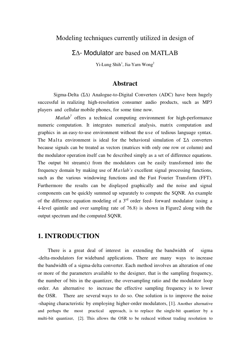
Fig. 1 shows the block diagram of a traditional third order 5-bit- modulator.
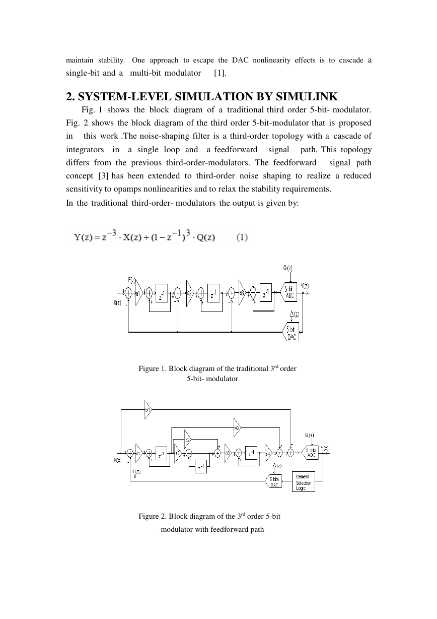
Fig. 2 shows the block diagram of the third order 5-bit-modulator that is proposed
in this work .The noise-shaping filter is a third-order topology with a cascade of
integrators in a single loop and a feedforward signal path. This topology
differs from the previous third-order-modulators. The feedforward signal path
concept [3] has been extended to third-order noise shaping to realize a reduced
sensitivity to opamps nonlinearities and to relax the stability requirements.
In the traditional third-order- modulators the output is given by:
Figure 1. Block diagram of the traditional 3rd order
5-bit- modulator
Figure 2. Block diagram of the 3rd order 5-bit
- modulator with feedforward path
�
The signal transfer function is STF(z) = z-3 and the noise transfer function is
NTF(z)=(1-z-1)3. In this case the harmonics of the input signal created due to the
nonlinear opamps will appear at the modulator output shaped by third-order
high-pass transfer function. In wideband applications, the attenuation provided by a
order high-pass transfer function at a low oversampling ratio is not enough. One
3
solution is to design low distortion opamps.
rd
In the-modulator with feedforward path the nonlinearity problem is achieved
by making the signal transfer function, STF(z) exactly equal to 1.
The proposed topology combines the advantage of sigma-delta modulator with
feedforward path and the multibit quantizer to achieve high dynamic range and
wideband A/D conversion.This topology uses only one DAC in the feedback path.
This advantage is very important for multibit quantizer because of this reduces
the complexity of circuit and the chip area. Another advantage of this topology
is that the integrators process quantization noise only and than their performance
requirements are relaxed.
By applying linear analysis, the output of the third orde-modulator with
feedforward path is given by
where the signal transfer function must be STF(z)=1, without changing the
third-order noise transfer function, NTF(z).
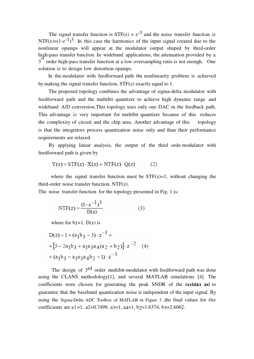
The noise transfer function for the topology presented in Fig. 1 is:
where for b1=1, D(z) is
The design of 3rd order multibit-modulator with feedforward path was done
using the CLANS methodology[1], and several MATLAB simulations [4]. The
coefficients were chosen for generating the peak SNDR of the modulator and to
guarantee that the baseband quantization noise is independent of the input signal. By
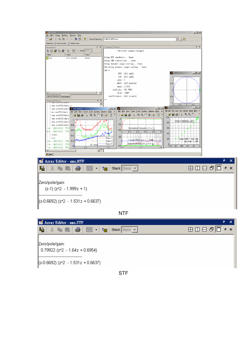
using the Sigma-Delta ADC Toolbox of MATLAB in Figure 3 ,the final values for th e
coefficients are a1 =1, a2=0.7499, a3=1, a4=1, b2=1.6374, b3=2.6062.
�
NTF
STF
�
Coefficients
Figure 3. Sigma-Delta ADC Toolbox of MATLAB
3. Simulation and Measure Result:
To further aid the designer, an empirical study of high order Σ∆-modulators
has been conducted and has resulted in a CAD toolbox (based in Matlab and freely
available) that allows Σ∆-modulator design and performance simulations to be carried
out with ease. In particular, the toolbox is comprised of various functions (written in
Matlab) that allow the user to synthesize different discrete noise transfer functions
and map these NTF onto different topologies so that the modulator coefficients can be
determined. A further function is also available to optimize the NTF for a low-pass
multi- bit Σ ∆ -modulator based on the “Closed-loop An al ys is of Noise-Shaper”
toolbox from
(CLANS) method from. This function uses
Matlab.Figure3 show the toolbox of ADC.Figure4 show the Third order Σ∆-modulator
CIFB Structure, and Figure5 and Figure6 show the results of waveform of simulation
and measure . Figure7 and Figure8 show the results of Frequency response of
simulation and measure.
the optimization
Figure 4. Third order Σ∆-modulator CIFB Structure
�
Figure 5. MATLAB simulation waveform
Figure 6. measure waveform
Figure 7. Frequency response by using Matlab
Figure 8. Frequency response of Implement by circuits
�
REFERENCES
[1]S.R.Norsworthy, R.Schreier and G.C. Temes, Delta-Sigma Converters-Theory, Design and
Simulation, New York: IEEE Press, 1997, pp.
244-278.
[2] M. R. Miller and C. S. Perie, “A Multi-Bit Sigma-Delta ADC for Multi-Mode Receivers”,
in Proc. IEEE Custom Integrated Circuits Conference, 2002, pp. 191-194.
[3] J. Silva, U. J. Moon and G. C. Temes, “Wideband low-distortion delta-sigma ADC
topology” , IEE Electronics Letters, no. 12, pp.
737-738, Jun. 2001.
[4] P.G.A. Jespers, “Integrated converters: D to A and A to D Architecture, Analysis and
�




 2023年江西萍乡中考道德与法治真题及答案.doc
 2012年重庆南川中考生物真题及答案.doc
 2013年江西师范大学地理学综合及文艺理论基础考研真题.doc
 2020年四川甘孜小升初语文真题及答案I卷.doc
 2020年注册岩土工程师专业基础考试真题及答案.doc
 2023-2024学年福建省厦门市九年级上学期数学月考试题及答案.doc
 2021-2022学年辽宁省沈阳市大东区九年级上学期语文期末试题及答案.doc
 2022-2023学年北京东城区初三第一学期物理期末试卷及答案.doc
 2018上半年江西教师资格初中地理学科知识与教学能力真题及答案.doc
 2012年河北国家公务员申论考试真题及答案-省级.doc
 2020-2021学年江苏省扬州市江都区邵樊片九年级上学期数学第一次质量检测试题及答案.doc
 2022下半年黑龙江教师资格证中学综合素质真题及答案.doc