Preliminary User’s Manual
μPD79F9211
16-bit Single-Chip Microcontrollers
Date Published February 2008 NS CP(K)
Printed in Japan
2008
�
[MEMO]
2
Preliminary User’s Manual
�
NOTES FOR CMOS DEVICES
1
2
3
4
5
6
VOLTAGE APPLICATION WAVEFORM AT INPUT PIN
Waveform distortion due to input noise or a reflected wave may cause malfunction. If the input of the
CMOS device stays in the area between VIL (MAX) and VIH (MIN) due to noise, etc., the device may
malfunction. Take care to prevent chattering noise from entering the device when the input level is fixed,
and also in the transition period when the input level passes through the area between VIL (MAX) and
VIH (MIN).
HANDLING OF UNUSED INPUT PINS
Unconnected CMOS device inputs can be cause of malfunction. If an input pin is unconnected, it is
possible that an internal input level may be generated due to noise, etc., causing malfunction. CMOS
devices behave differently than Bipolar or NMOS devices. Input levels of CMOS devices must be fixed
high or low by using pull-up or pull-down circuitry. Each unused pin should be connected to VDD or GND
via a resistor if there is a possibility that it will be an output pin. All handling related to unused pins must
be judged separately for each device and according to related specifications governing the device.
PRECAUTION AGAINST ESD
A strong electric field, when exposed to a MOS device, can cause destruction of the gate oxide and
ultimately degrade the device operation. Steps must be taken to stop generation of static electricity as
much as possible, and quickly dissipate it when it has occurred. Environmental control must be
adequate. When it is dry, a humidifier should be used. It is recommended to avoid using insulators that
easily build up static electricity. Semiconductor devices must be stored and transported in an anti-static
container, static shielding bag or conductive material. All test and measurement tools including work
benches and floors should be grounded. The operator should be grounded using a wrist strap.
Semiconductor devices must not be touched with bare hands. Similar precautions need to be taken for
PW boards with mounted semiconductor devices.
STATUS BEFORE INITIALIZATION
Power-on does not necessarily define the initial status of a MOS device. Immediately after the power
source is turned ON, devices with reset functions have not yet been initialized. Hence, power-on does
not guarantee output pin levels, I/O settings or contents of registers. A device is not initialized until the
reset signal is received. A reset operation must be executed immediately after power-on for devices
with reset functions.
POWER ON/OFF SEQUENCE
In the case of a device that uses different power supplies for the internal operation and external
interface, as a rule, switch on the external power supply after switching on the internal power supply.
When switching the power supply off, as a rule, switch off the external power supply and then the
internal power supply. Use of the reverse power on/off sequences may result in the application of an
overvoltage to the internal elements of the device, causing malfunction and degradation of internal
elements due to the passage of an abnormal current.
The correct power on/off sequence must be judged separately for each device and according to related
specifications governing the device.
INPUT OF SIGNAL DURING POWER OFF STATE
Do not input signals or an I/O pull-up power supply while the device is not powered. The current
injection that results from input of such a signal or I/O pull-up power supply may cause malfunction and
the abnormal current that passes in the device at this time may cause degradation of internal elements.
Input of signals during the power off state must be judged separately for each device and according to
related specifications governing the device.
Preliminary User’s Manual
3
�
Windows and Windows NT are registered trademarks or trademarks of Microsoft Corporation in the United
States and/or other countries.
PC/AT is a trademark of International Business Machines Corporation.
EEPROM is a trademark of NEC Electronics Corporation.
SuperFlash is a registered trademark of Silicon Storage Technology, Inc. in several countries including the
United States and Japan.
Caution: This product uses SuperFlash® technology licensed from Silicon Storage Technology, Inc.
•
•
•
•
•
•
•
The information contained in this document is being issued in advance of the production cycle for the
product. The parameters for the product may change before final production or NEC Electronics
Corporation, at its own discretion, may withdraw the product prior to its production.
Not all products and/or types are available in every country. Please check with an NEC Electronics sales
representative for availability and additional information.
No part of this document may be copied or reproduced in any form or by any means without the prior written consent
of NEC Electronics. NEC Electronics assumes no responsibility for any errors that may appear in this document.
NEC Electronics does not assume any liability for infringement of patents, copyrights or other intellectual property
rights of third parties by or arising from the use of NEC Electronics products listed in this document or any other
liability arising from the use of such products. No license, express, implied or otherwise, is granted under any
patents, copyrights or other intellectual property rights of NEC Electronics or others.
Descriptions of circuits, software and other related information in this document are provided for illustrative purposes
in semiconductor product operation and application examples. The incorporation of these circuits, software and
information in the design of a customer's equipment shall be done under the full responsibility of the customer. NEC
Electronics assumes no responsibility for any losses incurred by customers or third parties arising from the use of
these circuits, software and information.
While NEC Electronics endeavors to enhance the quality, reliability and safety of NEC Electronics products,
customers agree and acknowledge that the possibility of defects thereof cannot be eliminated entirely. To minimize
risks of damage to property or injury (including death) to persons arising from defects in NEC Electronics products,
customers must incorporate sufficient safety measures in their design, such as redundancy, fire-containment and
anti-failure features.
NEC Electronics products are classified into the following three quality grades: "Standard", "Special" and "Specific".
The "Specific" quality grade applies only to NEC Electronics products developed based on a customer-designated
"quality assurance program" for a specific application. The recommended applications of an NEC Electronics
products depend on its quality grade, as indicated below. Customers must check the quality grade of each NEC
Electronics product before using it in a particular application.
"Standard":
Computers, office equipment, communications equipment, test and measurement equipment, audio and
visual equipment, home electronic appliances, machine tools, personal electronic equipment and
industrial robots.
Transportation equipment (automobiles, trains, ships, etc.), traffic control systems, anti-disaster
systems, anti-crime systems, safety equipment and medical equipment (not specifically designed for life
support).
Aircraft, aerospace equipment, submersible repeaters, nuclear reactor control systems, life support
systems and medical equipment for life support, etc.
"Special":
"Specific":
The quality grade of NEC Electronics products is "Standard" unless otherwise expressly specified in NEC
Electronics data sheets or data books, etc. If customers wish to use NEC Electronics products in applications
not intended by NEC Electronics, they must contact an NEC Electronics sales representative in advance to
determine NEC Electronics' willingness to support a given application.
(Note)
(1)
(2)
4
"NEC Electronics" as used in this statement means NEC Electronics Corporation and also includes its
majority-owned subsidiaries.
"NEC Electronics products" means any product developed or manufactured by or for NEC Electronics (as
defined above).
Preliminary User’s Manual
M5D 02. 11-1
�
INTRODUCTION
Readers
Purpose
Organization
How to Read This Manual
This manual is intended for user engineers who wish to understand the functions of the
μPD79F9211 and design and develop application systems and programs for these
devices.
The target products are as follows.
μPD79F9210, μPD79F9211
This manual is intended to give users an understanding of the functions described in the
Organization below.
The μPD79F9211 manual is separated into two parts: this manual and the instructions
edition (common to the 78K0R Microcontroller Series).
μPD79F9211
User’s Manual
(This Manual)
78K0R Microcontroller
User’s Manual
Instructions
• Pin functions
• Internal block functions
• Interrupts
• Other on-chip peripheral functions
• Electrical specifications (target)
• CPU functions
• Instruction set
• Explanation of each instruction
It is assumed that the readers of this manual have general knowledge of electrical
engineering, logic circuits, and microcontrollers.
• To gain a general understanding of functions:
→ Read this manual in the order of the CONTENTS.
• How to interpret the register format:
→ For a bit number enclosed in angle brackets, the bit name is defined as a
reserved word in the RA78K0R, and is defined as an sfr variable using the
#pragma sfr directive in the CC78K0R.
• To know details of the 78K0R Series instructions:
→ Refer to the separate document 78K0R Microcontroller Instructions User’s
Manual (U17792E).
Preliminary User’s Manual
5
�
Conventions
Related Documents
Higher digits on the left and lower digits on the right
Data significance:
Active low representations: ××× (overscore over pin and signal name)
Note:
Caution:
Remark:
Numerical representations: Binary
Footnote for item marked with Note in the text
Information requiring particular attention
Supplementary information
Decimal
Hexadecimal
...×××× or ××××B
...××××
...××××H
The related documents indicated in this publication may include preliminary versions.
However, preliminary versions are not marked as such.
Documents Related to Devices
μPD79F9211 User’s Manual
78K0R Microcontroller Instructions User’s Manual
Document Name
Documents Related to Development Tools (Software) (User’s Manuals)
Document No.
This manual
U17792E
Document Name
Document No.
CC78K0R Ver. 1.00 C Compiler
RA78K0R Ver. 1.00 Assembler Package
SM+ System Simulator
PM+ Ver. 6.20
ID78K0R-QB Ver. 3.20 Integrated Debugger
Operation
Language
Operation
Language
Operation
Operation
Documents Related to Development Tools (Hardware) (User’s Manuals)
Document Name
QB-MINI2 On-Chip Debug Emulator with Programming Function
QB-78K0RKX3L In-Circuit Emulator
Documents Related to Flash Memory Programming
Document Name
PG-FP4 Flash Memory Programmer User’s Manual
PG-FP5 Flash Memory Programmer User’s Manual
U17838E
U17837E
U17836E
U17835E
U18010E
U17990E
U17839E
Document No.
U18371E
To be prepared
Document No.
U15260E
U18865E
Caution The related documents listed above are subject to change without notice. Be sure to use the latest
version of each document when designing.
6
Preliminary User’s Manual
�
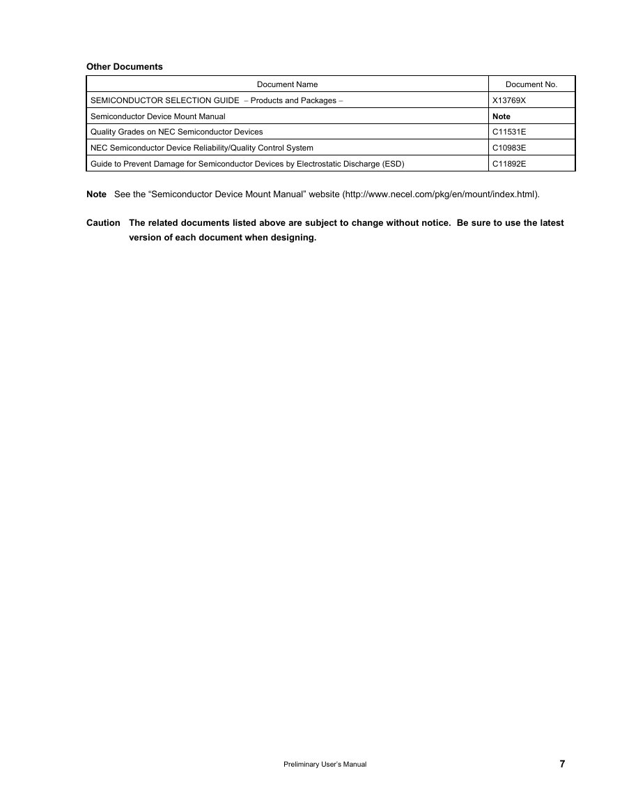
Other Documents
Document Name
Document No.
SEMICONDUCTOR SELECTION GUIDE − Products and Packages −
Semiconductor Device Mount Manual
Quality Grades on NEC Semiconductor Devices
NEC Semiconductor Device Reliability/Quality Control System
Guide to Prevent Damage for Semiconductor Devices by Electrostatic Discharge (ESD)
X13769X
Note
C11531E
C10983E
C11892E
Note See the “Semiconductor Device Mount Manual” website (http://www.necel.com/pkg/en/mount/index.html).
Caution The related documents listed above are subject to change without notice. Be sure to use the latest
version of each document when designing.
Preliminary User’s Manual
7
�
CONTENTS
CHAPTER 1 OUTLINE ............................................................................................................................ 18
1.1 Features......................................................................................................................................... 19
1.2 Applications.................................................................................................................................. 20
1.3 Ordering Information.................................................................................................................... 20
1.4 Pin Configuration (Top View) ...................................................................................................... 21
1.5 Block Diagram .............................................................................................................................. 23
1.6 Outline of Functions..................................................................................................................... 24
CHAPTER 2 PIN FUNCTIONS ............................................................................................................... 26
2.1 Pin Function List .......................................................................................................................... 26
2.2 Description of Pin Functions ...................................................................................................... 31
2.2.1 P10 to P13 (port 1)........................................................................................................................... 31
2.2.2 P20 to P27 (port 2)........................................................................................................................... 31
2.2.3 P30 to P32 (port 3)........................................................................................................................... 31
2.2.4 P40 and P41 (port 4)........................................................................................................................ 33
2.2.5 P50 to P52 (port 5)........................................................................................................................... 33
2.2.6 P70 to P75 (port 7)........................................................................................................................... 34
2.2.7 P80 to P83 (port 8)........................................................................................................................... 35
2.2.8 P120 to P124 (port 12)..................................................................................................................... 36
2.2.9 P150 and P151 (port 15).................................................................................................................. 36
2.2.10 AVREF.............................................................................................................................................. 37
2.2.11 AVSS ............................................................................................................................................... 37
2.2.12 RESET ........................................................................................................................................... 37
2.2.13 REGC............................................................................................................................................. 38
2.2.14 VDD ................................................................................................................................................. 38
2.2.15 VSS.................................................................................................................................................. 38
2.2.16 FLMD0 ........................................................................................................................................... 38
2.3 Pin I/O Circuits and Recommended Connection of Unused Pins ........................................... 39
CHAPTER 3 CPU ARCHITECTURE ...................................................................................................... 45
3.1 Memory Space .............................................................................................................................. 45
3.1.1 Internal program memory space ...................................................................................................... 48
3.1.2 Mirror area........................................................................................................................................ 50
3.1.3 Internal data memory space............................................................................................................. 51
3.1.4 Special function register (SFR) area ................................................................................................ 52
8
Preliminary User’s Manual U19120EJ1V0UD
�




 2023年江西萍乡中考道德与法治真题及答案.doc
 2012年重庆南川中考生物真题及答案.doc
 2013年江西师范大学地理学综合及文艺理论基础考研真题.doc
 2020年四川甘孜小升初语文真题及答案I卷.doc
 2020年注册岩土工程师专业基础考试真题及答案.doc
 2023-2024学年福建省厦门市九年级上学期数学月考试题及答案.doc
 2021-2022学年辽宁省沈阳市大东区九年级上学期语文期末试题及答案.doc
 2022-2023学年北京东城区初三第一学期物理期末试卷及答案.doc
 2018上半年江西教师资格初中地理学科知识与教学能力真题及答案.doc
 2012年河北国家公务员申论考试真题及答案-省级.doc
 2020-2021学年江苏省扬州市江都区邵樊片九年级上学期数学第一次质量检测试题及答案.doc
 2022下半年黑龙江教师资格证中学综合素质真题及答案.doc