THE I2C-BUS SPECIFICATION
VERSION 2.1
JANUARY 2000
�
Philips Semiconductors
The I2C-bus specification
CONTENTS
1
1.1
1.2
1.3
1.4
2
2.1
2.2
3
4
5
6
6.1
6.2
7
7.1
7.2
8
8.1
8.2
8.3
9
10
10.1
10.1.1
10.1.2
10.1.3
11
12
13
13.1
13.2
13.3
PREFACE . . . . . . . . . . . . . . . . . . . . . . . . . . .3
Version 1.0 - 1992. . . . . . . . . . . . . . . . . . . . 3
Version 2.0 - 198. . . . . . . . . . . . . . . . . . . . . 3
Version 2.1 - 1999. . . . . . . . . . . . . . . . . . . . 3
Purchase of Philips I2C-bus components . . 3
THE I2C-BUS BENEFITS DESIGNERS
AND MANUFACTURERS. . . . . . . . . . . . . . .4
Designer benefits . . . . . . . . . . . . . . . . . . . . 4
Manufacturer benefits . . . . . . . . . . . . . . . . . 6
INTRODUCTION TO THE I2C-BUS
SPECIFICATION . . . . . . . . . . . . . . . . . . . . .6
THE I2C-BUS CONCEPT . . . . . . . . . . . . . . .6
GENERAL CHARACTERISTICS . . . . . . . . .8
BIT TRANSFER . . . . . . . . . . . . . . . . . . . . . .8
Data validity . . . . . . . . . . . . . . . . . . . . . . . . 8
START and STOP conditions . . . . . . . . . . . 9
TRANSFERRING DATA . . . . . . . . . . . . . . .10
Byte format . . . . . . . . . . . . . . . . . . . . . . . . 10
Acknowledge. . . . . . . . . . . . . . . . . . . . . . . 10
ARBITRATION AND CLOCK
GENERATION . . . . . . . . . . . . . . . . . . . . . .11
Synchronization . . . . . . . . . . . . . . . . . . . . 11
Arbitration . . . . . . . . . . . . . . . . . . . . . . . . . 12
Use of the clock synchronizing
mechanism as a handshake . . . . . . . . . . . 13
FORMATS WITH 7-BIT ADDRESSES . . . .13
7-BIT ADDRESSING . . . . . . . . . . . . . . . . .15
Definition of bits in the first byte . . . . . . . . 15
General call address . . . . . . . . . . . . . . . . . 16
START byte . . . . . . . . . . . . . . . . . . . . . . . 17
CBUS compatibility . . . . . . . . . . . . . . . . . . 18
EXTENSIONS TO THE STANDARD-
MODE I2C-BUS SPECIFICATION . . . . . . .19
FAST-MODE. . . . . . . . . . . . . . . . . . . . . . . .19
Hs-MODE . . . . . . . . . . . . . . . . . . . . . . . . . .20
High speed transfer. . . . . . . . . . . . . . . . . . 20
Serial data transfer format in Hs-mode . . . 21
Switching from F/S- to Hs-mode and
back . . . . . . . . . . . . . . . . . . . . . . . . . . . . . 23
2
13.4
13.5
13.5.1
13.5.2
13.5.3
14
14.1
14.2
14.3
15
15.1
15.2
16
16.1
17
17.1
17.2
17.3
17.4
17.5
18
18.1
18.1.1
19
20
Hs-mode devices at lower speed modes. . 24
Mixed speed modes on one serial bus
system . . . . . . . . . . . . . . . . . . . . . . . . . . . . 24
F/S-mode transfer in a mixed-speed bus
system . . . . . . . . . . . . . . . . . . . . . . . . . . . . 25
Hs-mode transfer in a mixed-speed bus
system . . . . . . . . . . . . . . . . . . . . . . . . . . . . 25
Timing requirements for the bridge in a
mixed-speed bus system . . . . . . . . . . . . . . 27
10-BIT ADDRESSING . . . . . . . . . . . . . . . . 27
Definition of bits in the first two bytes. . . . . 27
Formats with 10-bit addresses. . . . . . . . . . 27
General call address and start byte with
10-bit addressing . . . . . . . . . . . . . . . . . . . . 30
ELECTRICAL SPECIFICATIONS
AND TIMING FOR I/O STAGES
AND BUS LINES . . . . . . . . . . . . . . . . . . . . 30
Standard- and Fast-mode devices. . . . . . . 30
Hs-mode devices . . . . . . . . . . . . . . . . . . . . 34
ELECTRICAL CONNECTIONS OF
I2C-BUS DEVICES TO THE BUS LINES . 37
Maximum and minimum values of
resistors Rp and Rs for Standard-mode
I2C-bus devices . . . . . . . . . . . . . . . . . . . . . 39
APPLICATION INFORMATION . . . . . . . . . 41
Slope-controlled output stages of
Fast-mode I2C-bus devices . . . . . . . . . . . . 41
Switched pull-up circuit for Fast-mode
I2C-bus devices . . . . . . . . . . . . . . . . . . . . . 41
Wiring pattern of the bus lines . . . . . . . . . . 42
Maximum and minimum values of
resistors Rp and Rs for Fast-mode
I2C-bus devices . . . . . . . . . . . . . . . . . . . . . 42
Maximum and minimum values of
resistors Rp and Rs for Hs-mode
I2C-bus devices . . . . . . . . . . . . . . . . . . . . . 42
BI-DIRECTIONAL LEVEL SHIFTER
FOR F/S-MODE I2C-BUS SYSTEMS . . . . 42
Connecting devices with different
logic levels . . . . . . . . . . . . . . . . . . . . . . . . . 43
Operation of the level shifter . . . . . . . . . . . 44
DEVELOPMENT TOOLS AVAILABLE
FROM PHILIPS . . . . . . . . . . . . . . . . . . . . . 45
SUPPORT LITERATURE . . . . . . . . . . . . . 46
�
Philips Semiconductors
The I2C-bus specification
1 PREFACE
1.1
Version 1.0 - 1992
This version of the 1992 I2C-bus specification includes the
following modifications:
• Programming of a slave address by software has been
omitted. The realization of this feature is rather
complicated and has not been used.
• The “low-speed mode” has been omitted. This mode is,
in fact, a subset of the total I2C-bus specification and
need not be specified explicitly.
• The Fast-mode is added. This allows a fourfold increase
of the bit rate up to 400 kbit/s. Fast-mode devices are
downwards compatible i.e. they can be used in a 0 to
100 kbit/s I2C-bus system.
• 10-bit addressing is added. This allows 1024 additional
slave addresses.
• Slope control and input filtering for Fast-mode devices is
specified to improve the EMC behaviour.
NOTE: Neither the 100 kbit/s I2C-bus system nor the
100 kbit/s devices have been changed.
1.2
Version 2.0 - 1998
The I2C-bus has become a de facto world standard that is
now implemented in over 1000 different ICs and licensed
to more than 50 companies. Many of today’s applications,
however, require higher bus speeds and lower supply
voltages. This updated version of the I2C-bus specification
meets those requirements and includes the following
modifications:
• The High-speed mode (Hs-mode) is added. This allows
an increase in the bit rate up to 3.4 Mbit/s. Hs-mode
devices can be mixed with Fast- and Standard-mode
devices on the one I2C-bus system with bit rates from 0
to 3.4 Mbit/s.
• The low output level and hysteresis of devices with a
supply voltage of 2 V and below has been adapted to
meet the required noise margins and to remain
compatible with higher supply voltage devices.
• The 0.6 V at 6 mA requirement for the output stages of
Fast-mode devices has been omitted.
• The fixed input levels for new devices are replaced by
bus voltage-related levels.
• Application information for bi-directional level shifter is
added.
1.3
Version 2.1 - 2000
Version 2.1 of the I2C-bus specification includes the
following minor modifications:
• After a repeated START condition in Hs-mode, it is
possible to stretch the clock signal SCLH (see
Section 13.2 and Figs 22, 25 and 32).
• Some timing parameters in Hs-mode have been relaxed
(see Tables 6 and 7).
1.4
Purchase of Philips I2C-bus components
Purchase of Philips I2C components conveys a license under the Philips’ I2C patent to use the
components in the I2C system provided the system conforms to the I2C specification defined by
Philips.
3
�
Philips Semiconductors
The I2C-bus specification
2
THE I2C-BUS BENEFITS DESIGNERS AND
MANUFACTURERS
In consumer electronics, telecommunications and
industrial electronics, there are often many similarities
between seemingly unrelated designs. For example,
nearly every system includes:
• Some intelligent control, usually a single-chip
microcontroller
• General-purpose circuits like LCD drivers, remote I/O
ports, RAM, EEPROM, or data converters
• Application-oriented circuits such as digital tuning and
signal processing circuits for radio and video systems, or
DTMF generators for telephones with tone dialling.
To exploit these similarities to the benefit of both systems
designers and equipment manufacturers, as well as to
maximize hardware efficiency and circuit simplicity, Philips
developed a simple bi-directional 2-wire bus for efficient
inter-IC control. This bus is called the Inter IC or I2C-bus.
At present, Philips’ IC range includes more than 150
CMOS and bipolar I2C-bus compatible types for
performing functions in all three of the previously
mentioned categories. All I2C-bus compatible devices
incorporate an on-chip interface which allows them to
communicate directly with each other via the I2C-bus. This
design concept solves the many interfacing problems
encountered when designing digital control circuits.
Here are some of the features of the I2C-bus:
• Only two bus lines are required; a serial data line (SDA)
and a serial clock line (SCL)
• Each device connected to the bus is software
addressable by a unique address and simple
master/slave relationships exist at all times; masters can
operate as master-transmitters or as master-receivers
• It’s a true multi-master bus including collision detection
and arbitration to prevent data corruption if two or more
masters simultaneously initiate data transfer
• Serial, 8-bit oriented, bi-directional data transfers can be
made at up to 100 kbit/s in the Standard-mode, up to
400 kbit/s in the Fast-mode, or up to 3.4 Mbit/s in the
High-speed mode
• On-chip filtering rejects spikes on the bus data line to
preserve data integrity
• The number of ICs that can be connected to the same
bus is limited only by a maximum bus capacitance of
400 pF.
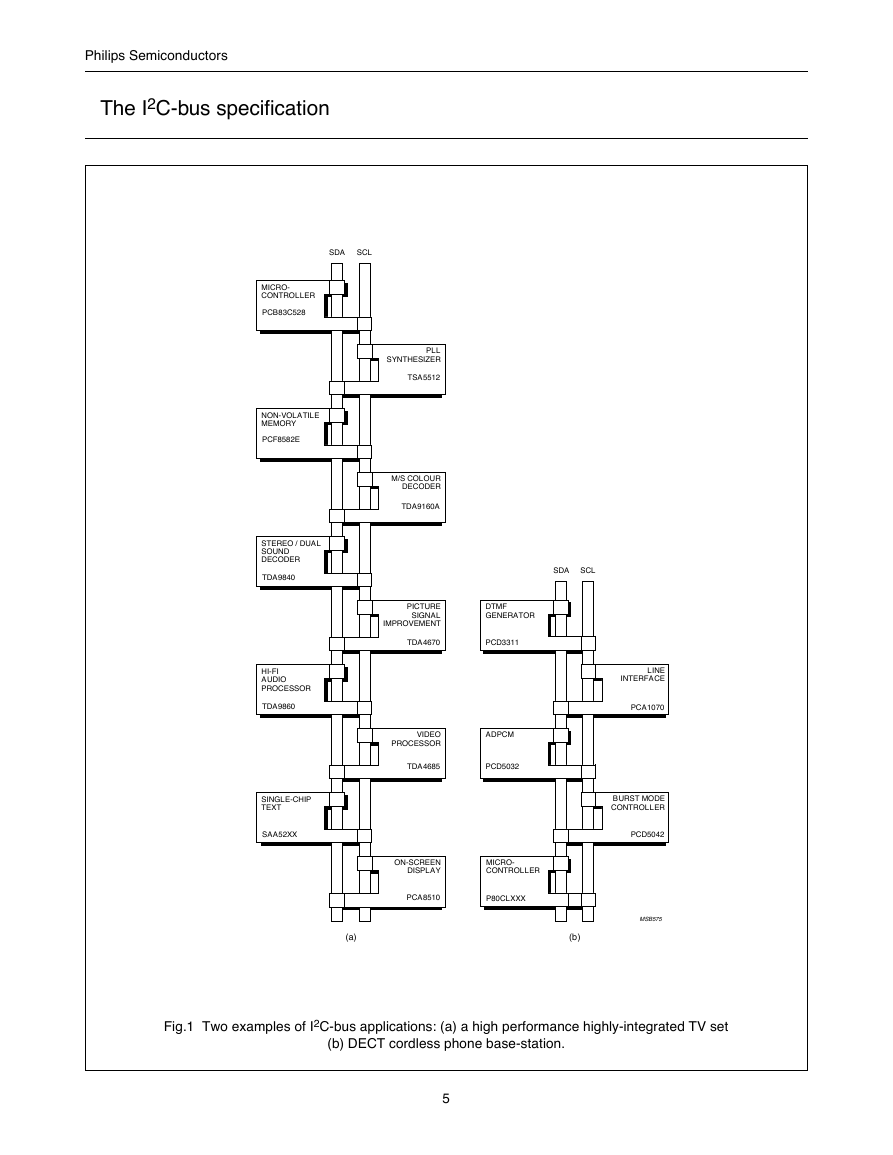
Figure 1 shows two examples of I2C-bus applications.
2.1
Designer benefits
I2C-bus compatible ICs allow a system design to rapidly
progress directly from a functional block diagram to a
prototype. Moreover, since they ‘clip’ directly onto the
I2C-bus without any additional external interfacing, they
allow a prototype system to be modified or upgraded
simply by ‘clipping’ or ‘unclipping’ ICs to or from the bus.
Here are some of the features of I2C-bus compatible ICs
which are particularly attractive to designers:
• Functional blocks on the block diagram correspond with
the actual ICs; designs proceed rapidly from block
diagram to final schematic.
• No need to design bus interfaces because the I2C-bus
interface is already integrated on-chip.
• Integrated addressing and data-transfer protocol allow
systems to be completely software-defined
• The same IC types can often be used in many different
applications
• Design-time reduces as designers quickly become
familiar with the frequently used functional blocks
represented by I2C-bus compatible ICs
• ICs can be added to or removed from a system without
affecting any other circuits on the bus
• Fault diagnosis and debugging are simple; malfunctions
can be immediately traced
• Software development time can be reduced by
assembling a library of reusable software modules.
In addition to these advantages, the CMOS ICs in the
I2C-bus compatible range offer designers special features
which are particularly attractive for portable equipment and
battery-backed systems.
They all have:
• Extremely low current consumption
• High noise immunity
• Wide supply voltage range
• Wide operating temperature range.
4
�
Philips Semiconductors
The I2C-bus specification
handbook, full pagewidth
SDA
SCL
MICRO-
CONTROLLER
PCB83C528
NON-VOLATILE
MEMORY
PCF8582E
STEREO / DUAL
SOUND
DECODER
TDA9840
HI-FI
AUDIO
PROCESSOR
TDA9860
SINGLE-CHIP
TEXT
SAA52XX
PLL
SYNTHESIZER
TSA5512
M/S COLOUR
DECODER
TDA9160A
SDA SCL
PICTURE
SIGNAL
IMPROVEMENT
DTMF
GENERATOR
TDA4670
PCD3311
VIDEO
PROCESSOR
ADPCM
TDA4685
PCD5032
LINE
INTERFACE
PCA1070
BURST MODE
CONTROLLER
PCD5042
ON-SCREEN
DISPLAY
MICRO-
CONTROLLER
PCA8510
P80CLXXX
(a)
MSB575
(b)
Fig.1 Two examples of I2C-bus applications: (a) a high performance highly-integrated TV set
(b) DECT cordless phone base-station.
5
�
Philips Semiconductors
The I2C-bus specification
2.2
Manufacturer benefits
I2C-bus compatible ICs don’t only assist designers, they
also give a wide range of benefits to equipment
manufacturers because:
• The simple 2-wire serial I2C-bus minimizes
interconnections so ICs have fewer pins and there are
not so many PCB tracks; result - smaller and less
expensive PCBs
• The completely integrated I2C-bus protocol eliminates
the need for address decoders and other ‘glue logic’
• The multi-master capability of the I2C-bus allows rapid
testing and alignment of end-user equipment via
external connections to an assembly-line
• The availability of I2C-bus compatible ICs in SO (small
outline), VSO (very small outline) as well as DIL
packages reduces space requirements even more.
These are just some of the benefits. In addition, I2C-bus
compatible ICs increase system design flexibility by
allowing simple construction of equipment variants and
easy upgrading to keep designs up-to-date. In this way, an
entire family of equipment can be developed around a
basic model. Upgrades for new equipment, or
enhanced-feature models (i.e. extended memory, remote
control, etc.) can then be produced simply by clipping the
appropriate ICs onto the bus. If a larger ROM is needed,
it’s simply a matter of selecting a micro-controller with a
larger ROM from our comprehensive range. As new ICs
supersede older ones, it’s easy to add new features to
equipment or to increase its performance by simply
unclipping the outdated IC from the bus and clipping on its
successor.
3
INTRODUCTION TO THE I2C-BUS SPECIFICATION
For 8-bit oriented digital control applications, such as those
requiring microcontrollers, certain design criteria can be
established:
• A complete system usually consists of at least one
microcontroller and other peripheral devices such as
memories and I/O expanders
• The cost of connecting the various devices within the
system must be minimized
• A system that performs a control function doesn’t
require high-speed data transfer
• Overall efficiency depends on the devices chosen and
the nature of the interconnecting bus structure.
To produce a system to satisfy these criteria, a serial bus
structure is needed. Although serial buses don’t have the
throughput capability of parallel buses, they do require
less wiring and fewer IC connecting pins. However, a bus
is not merely an interconnecting wire, it embodies all the
formats and procedures for communication within the
system.
Devices communicating with each other on a serial bus
must have some form of protocol which avoids all
possibilities of confusion, data loss and blockage of
information. Fast devices must be able to communicate
with slow devices. The system must not be dependent on
the devices connected to it, otherwise modifications or
improvements would be impossible. A procedure has also
to be devised to decide which device will be in control of
the bus and when. And, if different devices with different
clock speeds are connected to the bus, the bus clock
source must be defined. All these criteria are involved in
the specification of the I2C-bus.
4
THE I2C-BUS CONCEPT
The I2C-bus supports any IC fabrication process (NMOS,
CMOS, bipolar). Two wires, serial data (SDA) and serial
clock (SCL), carry information between the devices
connected to the bus. Each device is recognized by a
unique address (whether it’s a microcontroller, LCD driver,
memory or keyboard interface) and can operate as either
a transmitter or receiver, depending on the function of the
device. Obviously an LCD driver is only a receiver,
whereas a memory can both receive and transmit data. In
addition to transmitters and receivers, devices can also be
considered as masters or slaves when performing data
transfers (see Table 1). A master is the device which
initiates a data transfer on the bus and generates the clock
signals to permit that transfer. At that time, any device
addressed is considered a slave.
6
�
Philips Semiconductors
The I2C-bus specification
Table 1 Definition of I2C-bus terminology
TERM
Transmitter
Receiver
Master
Slave
Multi-master
Arbitration
DESCRIPTION
The device which sends data to the
bus
The device which receives data from
the bus
The device which initiates a transfer,
generates clock signals and
terminates a transfer
The device addressed by a master
More than one master can attempt to
control the bus at the same time
without corrupting the message
Procedure to ensure that, if more
than one master simultaneously tries
to control the bus, only one is allowed
to do so and the winning message is
not corrupted
Synchronization Procedure to synchronize the clock
signals of two or more devices
The I2C-bus is a multi-master bus. This means that more
than one device capable of controlling the bus can be
connected to it. As masters are usually micro-controllers,
let’s consider the case of a data transfer between two
microcontrollers connected to the I2C-bus (see Fig.2).
This highlights the master-slave and receiver-transmitter
relationships to be found on the I2C-bus. It should be noted
that these relationships are not permanent, but only
depend on the direction of data transfer at that time. The
transfer of data would proceed as follows:
1) Suppose microcontroller A wants to send information to
microcontroller B:
• microcontroller A (master), addresses microcontroller B
(slave)
• microcontroller A (master-transmitter), sends data to
microcontroller B (slave- receiver)
• microcontroller A terminates the transfer
2) If microcontroller A wants to receive information from
microcontroller B:
• microcontroller A (master) addresses microcontroller B
(slave)
• microcontroller A (master- receiver) receives data from
microcontroller B (slave- transmitter)
• microcontroller A terminates the transfer.
Even in this case, the master (microcontroller A) generates
the timing and terminates the transfer.
The possibility of connecting more than one
microcontroller to the I2C-bus means that more than one
master could try to initiate a data transfer at the same time.
To avoid the chaos that might ensue from such an event -
an arbitration procedure has been developed. This
procedure relies on the wired-AND connection of all I2C
interfaces to the I2C-bus.
If two or more masters try to put information onto the bus,
the first to produce a ‘one’ when the other produces a
‘zero’ will lose the arbitration. The clock signals during
arbitration are a synchronized combination of the clocks
generated by the masters using the wired-AND connection
to the SCL line (for more detailed information concerning
arbitration see Section 8).
MICRO -
CONTROLLER
A
LCD
DRIVER
STATIC
RAM OR
EEPROM
SDA
SCL
GATE
ARRAY
ADC
MBC645
MICRO -
CONTROLLER
B
Fig.2 Example of an I2C-bus configuration using two microcontrollers.
7
�
Philips Semiconductors
The I2C-bus specification
Generation of clock signals on the I2C-bus is always the
responsibility of master devices; each master generates its
own clock signals when transferring data on the bus. Bus
clock signals from a master can only be altered when they
are stretched by a slow-slave device holding-down the
clock line, or by another master when arbitration occurs.
5 GENERAL CHARACTERISTICS
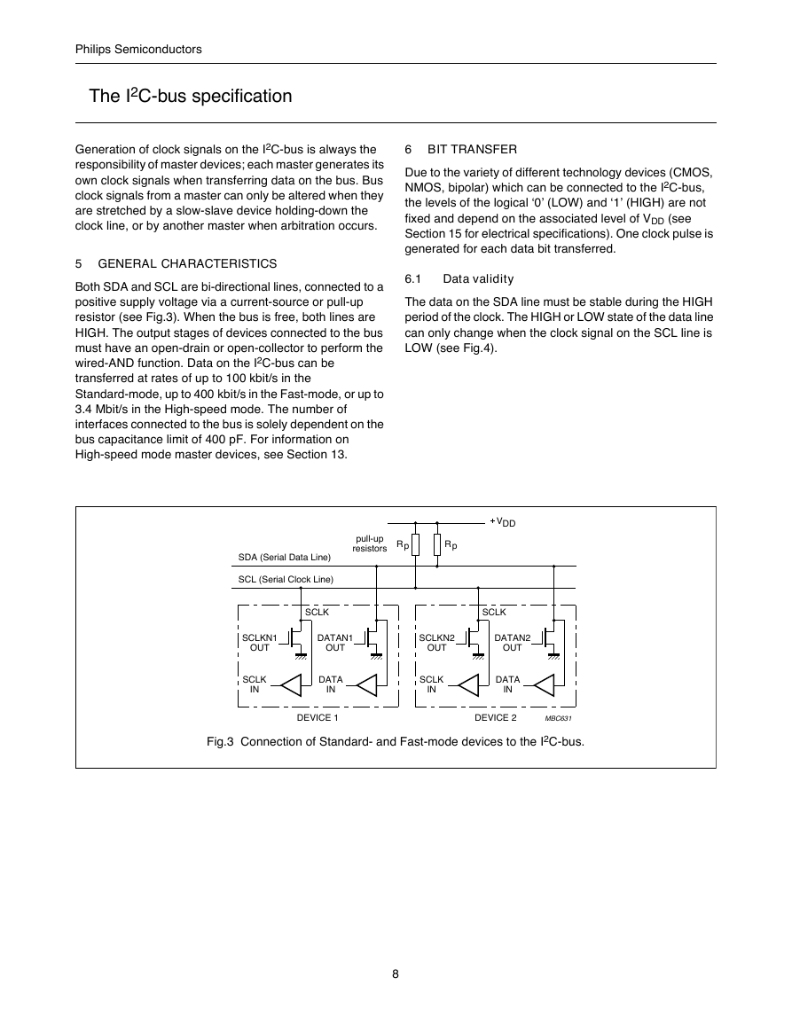
Both SDA and SCL are bi-directional lines, connected to a
positive supply voltage via a current-source or pull-up
resistor (see Fig.3). When the bus is free, both lines are
HIGH. The output stages of devices connected to the bus
must have an open-drain or open-collector to perform the
wired-AND function. Data on the I2C-bus can be
transferred at rates of up to 100 kbit/s in the
Standard-mode, up to 400 kbit/s in the Fast-mode, or up to
3.4 Mbit/s in the High-speed mode. The number of
interfaces connected to the bus is solely dependent on the
bus capacitance limit of 400 pF. For information on
High-speed mode master devices, see Section 13.
6 BIT TRANSFER
Due to the variety of different technology devices (CMOS,
NMOS, bipolar) which can be connected to the I2C-bus,
the levels of the logical ‘0’ (LOW) and ‘1’ (HIGH) are not
fixed and depend on the associated level of VDD (see
Section 15 for electrical specifications). One clock pulse is
generated for each data bit transferred.
6.1
Data validity
The data on the SDA line must be stable during the HIGH
period of the clock. The HIGH or LOW state of the data line
can only change when the clock signal on the SCL line is
LOW (see Fig.4).
pull-up
resistors
Rp
Rp
VDD
SDA (Serial Data Line)
SCL (Serial Clock Line)
SCLK
SCLK
SCLKN1
OUT
DATAN1
OUT
SCLKN2
OUT
DATAN2
OUT
SCLK
IN
DATA
IN
SCLK
IN
DATA
IN
DEVICE 1
DEVICE 2
MBC631
Fig.3 Connection of Standard- and Fast-mode devices to the I2C-bus.
8
�





 2023年江西萍乡中考道德与法治真题及答案.doc
 2012年重庆南川中考生物真题及答案.doc
 2013年江西师范大学地理学综合及文艺理论基础考研真题.doc
 2020年四川甘孜小升初语文真题及答案I卷.doc
 2020年注册岩土工程师专业基础考试真题及答案.doc
 2023-2024学年福建省厦门市九年级上学期数学月考试题及答案.doc
 2021-2022学年辽宁省沈阳市大东区九年级上学期语文期末试题及答案.doc
 2022-2023学年北京东城区初三第一学期物理期末试卷及答案.doc
 2018上半年江西教师资格初中地理学科知识与教学能力真题及答案.doc
 2012年河北国家公务员申论考试真题及答案-省级.doc
 2020-2021学年江苏省扬州市江都区邵樊片九年级上学期数学第一次质量检测试题及答案.doc
 2022下半年黑龙江教师资格证中学综合素质真题及答案.doc