2.4 GHz Inverted F Antenna
Keywords
• CC2400
• CC2420
• CC2430
• CC2431
• CC2500
• CC2510
1
Introduction
Design Note DN0007
By Audun Andersen
• CC2511
• CC2550
• PCB Antenna
• 2.4 GHz
•
Inverted F Antenna
This document describes a PCB antenna
design that can be used with all 2.4 GHz
transceivers and transmitters from Texas
Instruments. Maximum gain is measured
to be +3.3 dB and overall size
requirements for this antenna is 25.7 x 7.5
mm. Thus, this is a compact, low cost and
high performance antenna.
SWRU120
Page 1 of 15
�
Design Note DN0007
Table of Contents
KEYWORDS.............................................................................................................................. 1
INTRODUCTION............................................................................................................. 1
1
ABBREVIATIONS........................................................................................................... 2
2
3
DESCRIPTION OF THE INVERTED F ANTENNA DESIGN ......................................... 3
IMPLEMENTATION OF THE INVERTED F ANTENNA.......................................................... 3
4
RESULTS........................................................................................................................ 4
RADIATION PATTERN.................................................................................................. 4
REFLECTION ............................................................................................................ 11
BANDWIDTH............................................................................................................. 11
CONCLUSION .............................................................................................................. 12
REFERENCES.............................................................................................................. 13
GENERAL INFORMATION .......................................................................................... 14
DOCUMENT HISTORY................................................................................................ 14
IMPORTANT NOTICE .................................................................................................. 15
3.1
4.1
4.2
4.3
7.1
5
6
7
8
2
Abbreviations
EM
IFA
ISM
PCB
Evaluation Module
Inverted F Antenna
Industrial, Scientific, Medical
Printed Circuit Board
SWRU120
Page 2 of 15
�
Design Note DN0007
Description of the Inverted F Antenna Design
3
Since the impedance of the Inverted F Antenna is matched directly to 50 ohm no external
matching components are needed.
Implementation of the Inverted F Antenna
3.1
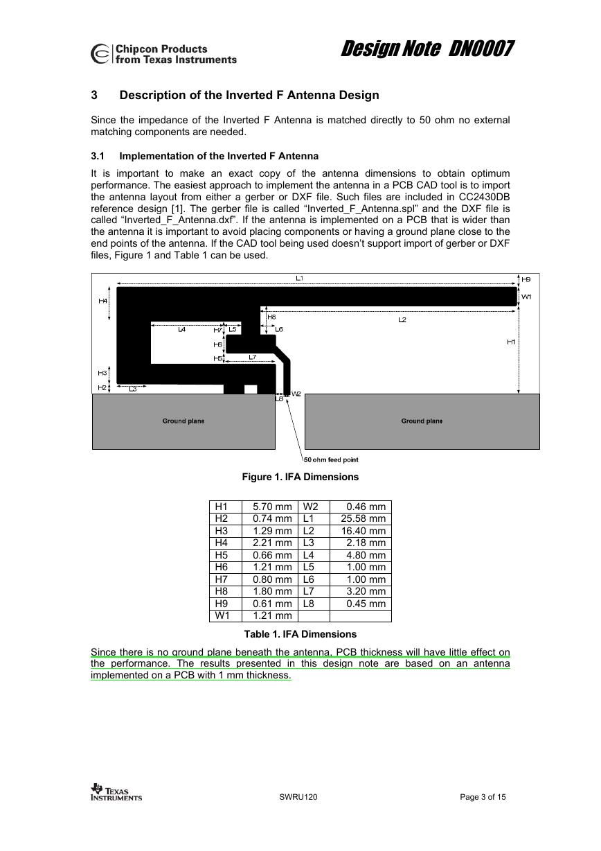
It is important to make an exact copy of the antenna dimensions to obtain optimum
performance. The easiest approach to implement the antenna in a PCB CAD tool is to import
the antenna layout from either a gerber or DXF file. Such files are included in CC2430DB
reference design [1]. The gerber file is called “Inverted_F_Antenna.spl” and the DXF file is
called “Inverted_F_Antenna.dxf”. If the antenna is implemented on a PCB that is wider than
the antenna it is important to avoid placing components or having a ground plane close to the
end points of the antenna. If the CAD tool being used doesn’t support import of gerber or DXF
files, Figure 1 and Table 1 can be used.
Figure 1. IFA Dimensions
H1
H2
H3
H4
H5
H6
H7
H8
H9
W1
5.70 mm W2
0.74 mm L1
1.29 mm L2
2.21 mm L3
0.66 mm L4
1.21 mm L5
0.80 mm L6
1.80 mm L7
0.61 mm L8
1.21 mm
0.46 mm
25.58 mm
16.40 mm
2.18 mm
4.80 mm
1.00 mm
1.00 mm
3.20 mm
0.45 mm
Table 1. IFA Dimensions
Since there is no ground plane beneath the antenna, PCB thickness will have little effect on
the performance. The results presented in this design note are based on an antenna
implemented on a PCB with 1 mm thickness.
SWRU120
Page 3 of 15
�
Design Note DN0007
4
Results
All results presented in this chapter are based on measurements performed with CC2430DB
[1].
4.1 Radiation Pattern
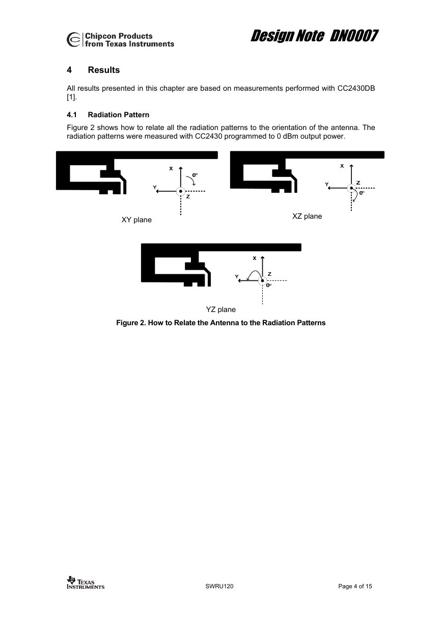
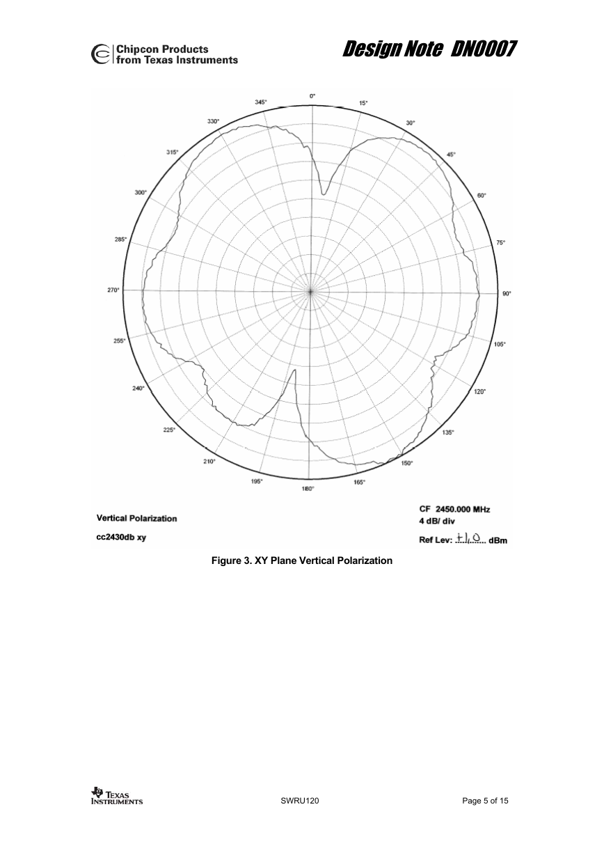
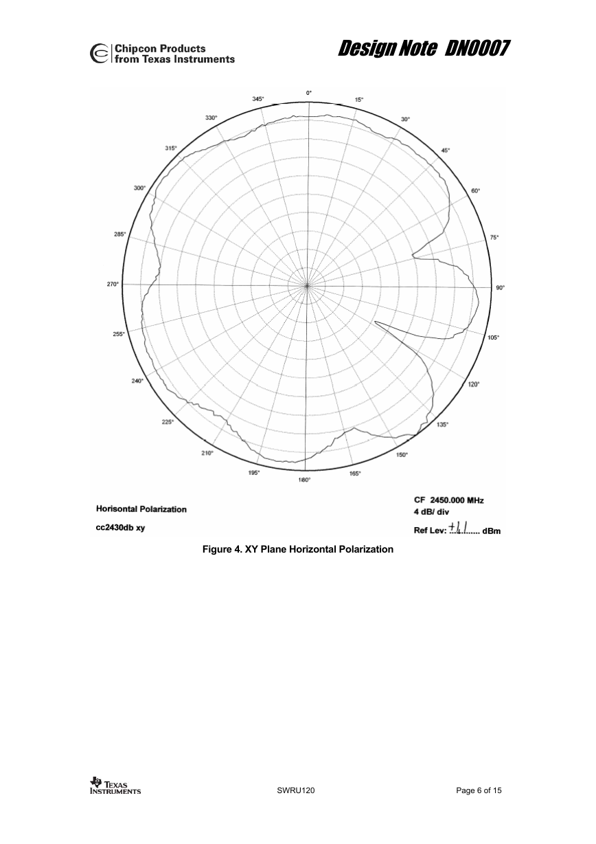
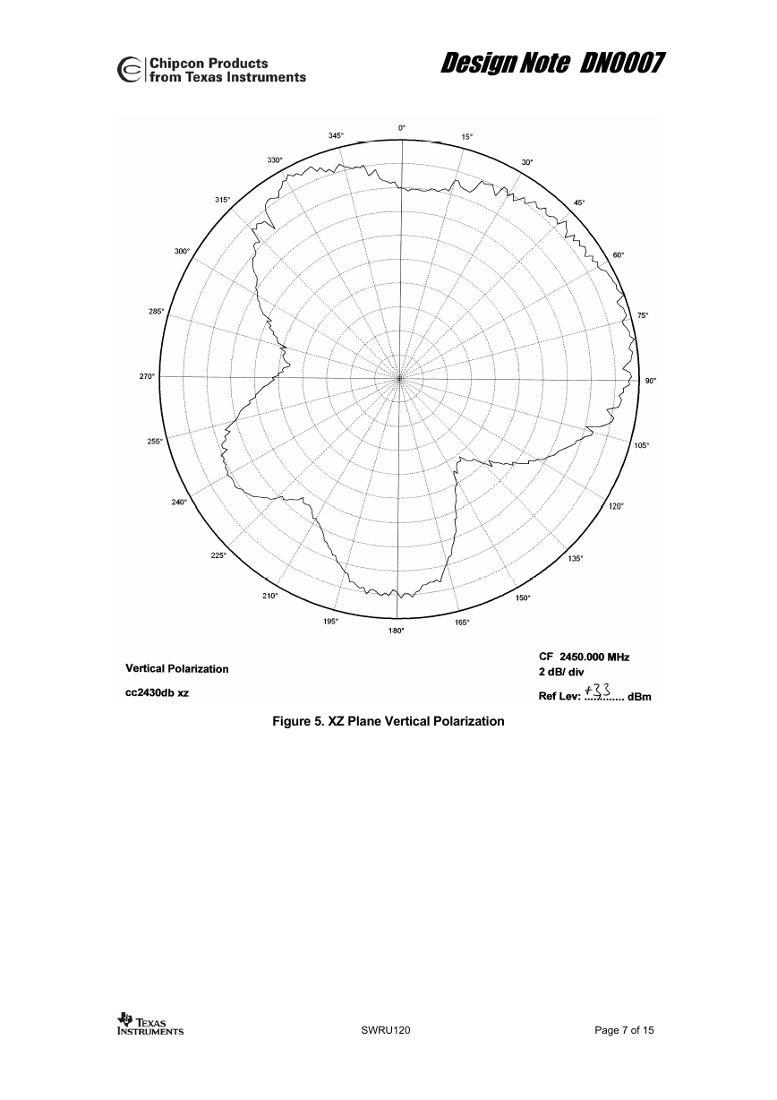
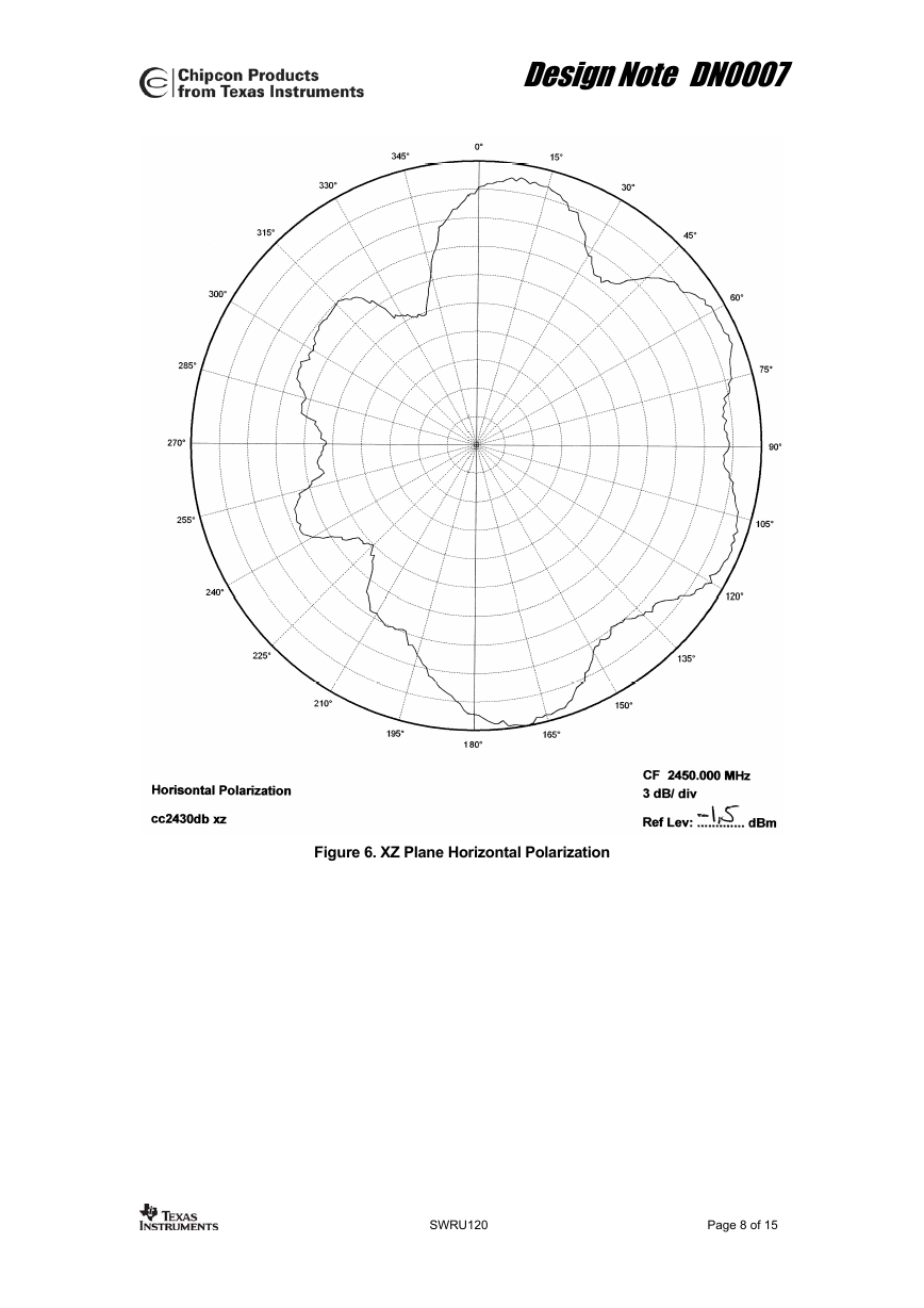
Figure 2 shows how to relate all the radiation patterns to the orientation of the antenna. The
radiation patterns were measured with CC2430 programmed to 0 dBm output power.
XY plane
XZ plane
YZ plane
Figure 2. How to Relate the Antenna to the Radiation Patterns
SWRU120
Page 4 of 15
�
Design Note DN0007
Figure 3. XY Plane Vertical Polarization
SWRU120
Page 5 of 15
�
Design Note DN0007
Figure 4. XY Plane Horizontal Polarization
SWRU120
Page 6 of 15
�
Design Note DN0007
Figure 5. XZ Plane Vertical Polarization
SWRU120
Page 7 of 15
�
Design Note DN0007
Figure 6. XZ Plane Horizontal Polarization
SWRU120
Page 8 of 15
�


 2023年江西萍乡中考道德与法治真题及答案.doc
 2012年重庆南川中考生物真题及答案.doc
 2013年江西师范大学地理学综合及文艺理论基础考研真题.doc
 2020年四川甘孜小升初语文真题及答案I卷.doc
 2020年注册岩土工程师专业基础考试真题及答案.doc
 2023-2024学年福建省厦门市九年级上学期数学月考试题及答案.doc
 2021-2022学年辽宁省沈阳市大东区九年级上学期语文期末试题及答案.doc
 2022-2023学年北京东城区初三第一学期物理期末试卷及答案.doc
 2018上半年江西教师资格初中地理学科知识与教学能力真题及答案.doc
 2012年河北国家公务员申论考试真题及答案-省级.doc
 2020-2021学年江苏省扬州市江都区邵樊片九年级上学期数学第一次质量检测试题及答案.doc
 2022下半年黑龙江教师资格证中学综合素质真题及答案.doc