eMMC4.51 LPDDR2 (H) MCP
Preliminary Data Sheet
80-36-03503
V0.3
March 2013
Corporate Headquarters • 951 SanDisk Drive • Milpitas, CA 95035
SanDisk Corporation
Phone (408) 801-1000 • Fax (408) 801-8657
www.sandisk.com
�
80-36-03503
REVISION HISTORY
SanDisk iNAND e.MMC 4.5 LPDDR2 MCP Preliminary Data Sheet
Doc. No
Revision
Date
Description
Reference
80-36-03503
0.1
16-October-2012
Preliminary
80-36-03503
0.2
22-January-2013
Updated corporate address
Updated iNAND and controller
content to latest discrete data
sheet
Updated package outline drawing
diagram to show measurement
letters
Fixed pinout ball naming
inconsistencies
Corrected package height in
Ordering Info table to 1.0mm
80-36-03503
0.3
05-March-2013
Reduced file size
SanDisk® Corporation general policy does not recommend the use of its products in life support applications where in a failure
or malfunction of the product may directly threaten life or injury. Per SanDisk Terms and Conditions of Sale, the user of SanDisk
products in life support applications assumes all risk of such use and indemnifies SanDisk against all damages. See “Disclaimer
of Liability.”
This document is for information use only and is subject to change without prior notice. SanDisk Corporation assumes no
responsibility for any errors that may appear in this document, nor for incidental or consequential damages resulting from the
furnishing, performance or use of this material. No part of this document may be reproduced, transmitted, transcribed, stored in
a retrievable manner or translated into any language or computer language, in any form or by any means, electronic,
mechanical, magnetic, optical, chemical, manual or otherwise, without the prior written consent of an officer of SanDisk
Corporation.
All parts of the SanDisk documentation are protected by copyright law and all rights are reserved.
SanDisk and the SanDisk logo are registered trademarks of SanDisk Corporation. Product names mentioned herein are for
identification purposes only and may be trademarks and/or registered trademarks of their respective companies.
© 2013 SanDisk Corporation. All rights reserved.
SanDisk products are covered or licensed under one or more of the following U.S. Patent Nos. 5,070,032; 5,095,344; 5,168,465;
5,172,338; 5,198,380; 5,200,959; 5,268,318; 5,268,870; 5,272,669; 5,418,752; 5,602,987. Other U.S. and foreign patents
awarded and pending.
80-36-03503. March 2013 Printed in the United States of America
© 2013 SanDisk Corporation
2
80-36-03503
�
80-36-03503
TABLE OF CONTENTS
Table of Contents
SanDisk iNAND e.MMC 4.5 LPDDR2 MCP Preliminary Data Sheet
1.
Introduction ......................................................................................................................... 5
1.1. General Description ...................................................................................................... 5
1.2. Plug-and-Play Integration ............................................................................................. 5
1.3. Features Overview ....................................................................................................... 6
1.4. Functional Description .................................................................................................. 7
1.5. Technology Independence ........................................................................................... 7
1.6. Defect and Error Management ...................................................................................... 7
1.7. MMC Bus and Power Lines .......................................................................................... 8
1.7.1. eMMC Bus Operating Conditions .................................................................................... 8
1.8. Low Power Mobile DDR Bus and Power Lines ............................................................. 9
1.8.1. Low Power Mobile DDR Bus Operating Conditions ...................................................... 11
1.8.2. DC Characteristics 1 (TJ = -30 C to +85 C, D-VDD and D-VDDQ = 1.7 V to 1.9 V, D-
VSS and D-VSSQ = 0 V) per DDR Die (4 Gbit Die) ................................................................... 14
1.8.3. Advanced Data Retention Current (TJ = 30 C to +85 C, D-VDD and D-VDDQ = 1.7
V to 1.9 V, D-VSS and D-VSSQ = 0 V) per DDR Die (4 Gbit Die) ............................................. 16
2. e.MMC4.51 Selected Features Overview .......................................................................... 17
2.1. Discard ....................................................................................................................... 17
2.2. Power Off Notifications ............................................................................................... 17
2.3. Packed Commands .................................................................................................... 17
2.4. Boot partitions Size ..................................................................................................... 17
2.5. Automatic Sleep Mode ................................................................................................ 17
2.6. Sleep (CMD5) ............................................................................................................. 18
2.7. Enhanced Reliable Write ............................................................................................ 18
2.8. Secure Erase .............................................................................................................. 18
2.9. Secure Trim ................................................................................................................ 19
2.10. Trim ............................................................................................................................ 19
2.11. Partition management................................................................................................. 19
2.12. Device Health ............................................................................................................. 19
2.13. Enhanced Write Protection ......................................................................................... 20
2.14. High Priority Interrupt (HPI)......................................................................................... 20
2.15. H/W Reset .................................................................................................................. 20
2.16. DDR I/F ...................................................................................................................... 20
3. Product Specifications ..................................................................................................... 21
3.1. Typical eMMC Power Requirements ........................................................................... 21
© 2013 SanDisk Corporation
3
80-36-03503
�
80-36-03503
Table of Contents
SanDisk iNAND e.MMC 4.5 LPDDR2 MCP Preliminary Data Sheet
3.2. Operating Conditions .................................................................................................. 22
3.2.1. Operating and Storage Temperature Specifications ..................................................... 22
3.2.2. Moisture Sensitivity ........................................................................................................ 22
3.3. System Performance .................................................................................................. 23
3.4. Physical Specifications ............................................................................................... 24
4.
Interface Description ......................................................................................................... 26
4.1.
iNAND MCP I/F Ball Array .......................................................................................... 26
4.2. Pins and Signal Description ........................................................................................ 26
4.3. Detailed LPDDR2 Block Diagram ............................................................................... 31
4.4.
iNAND Registers ........................................................................................................ 32
4.4.1. OCR Register................................................................................................................. 32
4.4.2. CID Register .................................................................................................................. 32
4.4.3. DSR Register ................................................................................................................. 32
4.4.4. CSD Register ................................................................................................................. 33
4.4.5. EXT_CSD Register ........................................................................................................ 34
5. Power Delivery and Capacitor Specifications ................................................................. 39
5.1. SanDisk iNAND LPDDR2 MCP eMMC Power Domains ............................................. 39
5.2. Capacitor Connection Guidelines ............................................................................... 39
5.2.1. VDDi Connections ......................................................................................................... 39
5.2.2. VCC and VCCQ Connections ........................................................................................ 39
6. Marking .............................................................................................................................. 41
7. Ordering Information ........................................................................................................ 42
A. Appendix A – 4Gbit DDR2 Mobile RAM Bare Chip .......................................................... 43
How to Contact Us ................................................................................................................ 169
© 2013 SanDisk Corporation
4
80-36-03503
�
80-36-03503
1. INTRODUCTION
Table of Contents
SanDisk iNAND e.MMC 4.5 LPDDR2 MCP Preliminary Data Sheet
1.1. General Description
iNAND MCP is an Embedded Flash Drive (EFD) and mobile DDR designed for mobile handsets
and consumer electronic devices. iNAND MCP is a hybrid device combining an embedded thin
flash controller and standard MLC NAND flash memory, with an industry standard e.MMC
4.511 interface and low power mobile DDR.
Empowered with a new e.MMC4.51 feature set such as Power Off Notifications and Packed
commands, as well as legacy e.MMC4.41 features such as Boot and RPMB partitions, HPI, and
HW Reset the iNAND MCP e.MMC is the optimal device for reliable code and data storage.
Designed specifically for mobile multimedia applications, iNAND MCP is the most mature on
board MMC device since 2005, providing mass storage of up to 128GB in JEDEC compatible
form factors, with low power consumption and high performance - an ideal solution for
multimedia handsets of 2.5G, 3G, 3.5G and 4G.
In addition to the high reliability and high system performance offered by the current iNAND
family of products, iNAND MCP offers plug-and-play integration and support for multiple
NAND technology transitions, as well as features such as advanced power management scheme.
iNAND MCP uses advanced Multi-Level Cell (MLC) NAND flash technology, enhanced by
SanDisk’s embedded flash management software running as firmware on the flash controller.
iNAND MCP architecture and embedded firmware fully emulates a hard disk to the host
processor, enabling read/write operations that are identical to a standard, sector-based hard drive.
In addition, SanDisk firmware employs patented methods, such as virtual mapping, dynamic and
static wear-leveling, and automatic block management to ensure high data reliability and
maximize flash life expectancy.
SanDisk iNAND MCP provides up to 4GB of memory for use in mass storage applications. In
addition to the mass-storage-specific flash memory chip, iNAND MCP includes an intelligent
controller, which manages interface protocols, data storage and retrieval, error correction code
(ECC) algorithms, defect handling and diagnostics, power management and clock control.
iNAND MCP enables multimedia driven applications such as music, photo, video, TV, GPS,
games, email, office and other applications.
The breakthrough in performance and design makes iNAND MCP the ideal solution for mobile
handset vendors, portable navigation and Automotive Infotainment vendors who require easy
integration, fast time to market and high-capacity.
1.2. Plug-and-Play Integration
iNAND MCP optimized architecture eliminates the need for complicated software integration
and testing processes and enables a practically plug-and-play integration in the system. The
replacement of one iNAND MCP device with another of a newer generation requires virtually no
changes to the host. This makes iNAND MCP the perfect solution for platforms and reference
1 Compatible to JESD84-B451
© 2013 SanDisk Corporation
5
80-36-03503
�
80-36-03503
Table of Contents
SanDisk iNAND e.MMC 4.5 LPDDR2 MCP Preliminary Data Sheet
designs, as it allows for the utilization of more advanced NAND Flash technology with minimal
integration or qualification efforts.
SanDisk iNAND MCP is well-suited to meet the needs of small, low power, electronic devices.
With JEDEC form factors measuring 11.5x13mm (162 balls) form factor compatible with 0.5mm
ball pitch, iNAND MCP is fit for a wide variety of portable devices such as multi-media mobile
handsets, personal media players, GPS devices and Automotive infotainment (car multimedia
and car navigation).
To support this wide range of applications, iNAND MCP is offered with an MMC Interface.
The MMC interface allows for easy integration into any design, regardless of the host (chipset)
type used. All device and interface configuration data (such as maximum frequency and device
identification) are stored on the device.
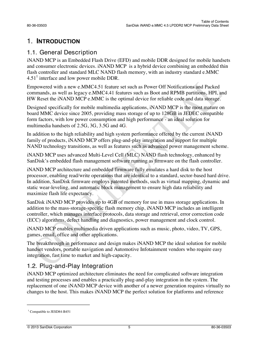
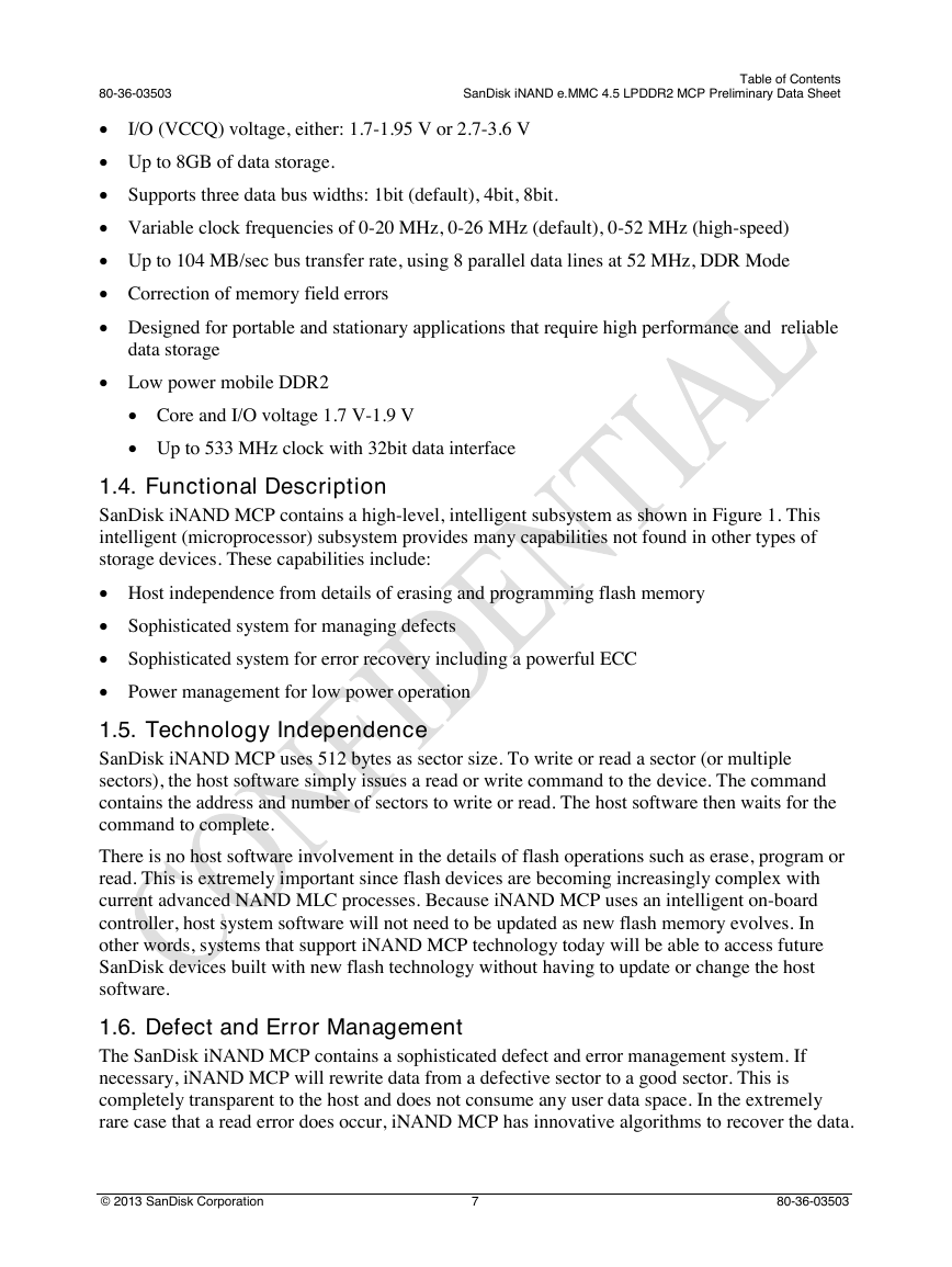
Figure 1 shows a block diagram of the SanDisk iNAND MCP.
Figure 1- SanDisk iNAND MCP Block Diagram
1.3. Features Overview
SanDisk iNAND MCP, with MMC and DDR interface, includes the following features:
Memory controller and NAND flash
Complies with e.MMC Specification Ver. 4.512
Mechanical design complies with JEDED MO-276C Specification
Offered in a TFBGA package of e.MMC 4.513
11.5mm x 13mm x 1.0mm
Operating temperature range: –25C° to +85C°
Dual power system
Core voltage (VCC) 2.7-3.6 V
2 Refer to JEDEC Standards No. JESD84-B451
3 Refer to JEDEC Standards No. JESD84-C441
© 2013 SanDisk Corporation
6
80-36-03503
�
80-36-03503
Table of Contents
SanDisk iNAND e.MMC 4.5 LPDDR2 MCP Preliminary Data Sheet
I/O (VCCQ) voltage, either: 1.7-1.95 V or 2.7-3.6 V
Up to 8GB of data storage.
Supports three data bus widths: 1bit (default), 4bit, 8bit.
Variable clock frequencies of 0-20 MHz, 0-26 MHz (default), 0-52 MHz (high-speed)
Up to 104 MB/sec bus transfer rate, using 8 parallel data lines at 52 MHz, DDR Mode
Correction of memory field errors
Designed for portable and stationary applications that require high performance and reliable
data storage
Low power mobile DDR2
Core and I/O voltage 1.7 V-1.9 V
Up to 533 MHz clock with 32bit data interface
1.4. Functional Description
SanDisk iNAND MCP contains a high-level, intelligent subsystem as shown in Figure 1. This
intelligent (microprocessor) subsystem provides many capabilities not found in other types of
storage devices. These capabilities include:
Host independence from details of erasing and programming flash memory
Sophisticated system for managing defects
Sophisticated system for error recovery including a powerful ECC
Power management for low power operation
1.5. Technology Independence
SanDisk iNAND MCP uses 512 bytes as sector size. To write or read a sector (or multiple
sectors), the host software simply issues a read or write command to the device. The command
contains the address and number of sectors to write or read. The host software then waits for the
command to complete.
There is no host software involvement in the details of flash operations such as erase, program or
read. This is extremely important since flash devices are becoming increasingly complex with
current advanced NAND MLC processes. Because iNAND MCP uses an intelligent on-board
controller, host system software will not need to be updated as new flash memory evolves. In
other words, systems that support iNAND MCP technology today will be able to access future
SanDisk devices built with new flash technology without having to update or change the host
software.
1.6. Defect and Error Management
The SanDisk iNAND MCP contains a sophisticated defect and error management system. If
necessary, iNAND MCP will rewrite data from a defective sector to a good sector. This is
completely transparent to the host and does not consume any user data space. In the extremely
rare case that a read error does occur, iNAND MCP has innovative algorithms to recover the data.
© 2013 SanDisk Corporation
7
80-36-03503
�
80-36-03503
Table of Contents
SanDisk iNAND e.MMC 4.5 LPDDR2 MCP Preliminary Data Sheet
These defect and error management systems, coupled with the solid state construction, give
SanDisk iNAND MCP unparalleled reliability.
1.7. MMC Bus and Power Lines
SanDisk iNAND MCP with MMC interface supports the MMC protocol. For more details
regarding these buses refer to JEDEC standards No. JESD84-B451.
The iNAND bus has the following communication and power lines:
CMD: Command is a bidirectional signal. The host and iNAND operate in two modes, open
drain and push-pull.
DAT0-7: Data lines are bidirectional signals. Host and iNAND operate in push-pull mode.
CLK: Clock input.
RST_n: Hardware Reset Input
VCCQ: VCCQ is the power supply line for host interface.
VCC: VCC is the power supply line for internal flash memory.
VDDi: VDDi is iNAND’s internal power node, not the power supply. Connect 0.1uF
capacitor from VDDi to ground.
VSS, VSSQ: ground lines.
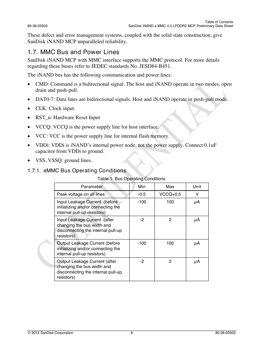
1.7.1. eMMC Bus Operating Conditions
Table 1: Bus Operating Conditions
Parameter
Peak voltage on all lines
Input Leakage Current (before
initializing and/or connecting the
internal pull-up resistors)
Input Leakage Current (after
changing the bus width and
disconnecting the internal pull-up
resistors)
Output Leakage Current (before
initializing and/or connecting the
internal pull-up resistors)
Output Leakage Current (after
changing the bus width and
disconnecting the internal pull-up
resistors)
Min
-0.5
-100
Max
Unit
VCCQ+0.5
100
V
µA
-2
2
µA
-100
100
µA
-2
2
µA
8
© 2013 SanDisk Corporation
80-36-03503
�




 2023年江西萍乡中考道德与法治真题及答案.doc
 2012年重庆南川中考生物真题及答案.doc
 2013年江西师范大学地理学综合及文艺理论基础考研真题.doc
 2020年四川甘孜小升初语文真题及答案I卷.doc
 2020年注册岩土工程师专业基础考试真题及答案.doc
 2023-2024学年福建省厦门市九年级上学期数学月考试题及答案.doc
 2021-2022学年辽宁省沈阳市大东区九年级上学期语文期末试题及答案.doc
 2022-2023学年北京东城区初三第一学期物理期末试卷及答案.doc
 2018上半年江西教师资格初中地理学科知识与教学能力真题及答案.doc
 2012年河北国家公务员申论考试真题及答案-省级.doc
 2020-2021学年江苏省扬州市江都区邵樊片九年级上学期数学第一次质量检测试题及答案.doc
 2022下半年黑龙江教师资格证中学综合素质真题及答案.doc