RK1808 Datasheet Rev 1.2
Rockchip
RK1808
Datasheet
Revision 1.2
May. 2019
Copyright 2019 ©Fuzhou Rockchip Electronics Co., Ltd. 1
�
RK1808 Datasheet Rev 1.2
Date
Revision
Revision History
Description
2019-5-27
1.2
Update
2019-3-1
1.1
Update DDR3 capacity from 2GB to 4GB
Update package thickness
2018-11-8
1.0
Initial released
Copyright 2019 ©Fuzhou Rockchip Electronics Co., Ltd. 2
�
RK1808 Datasheet Rev 1.2
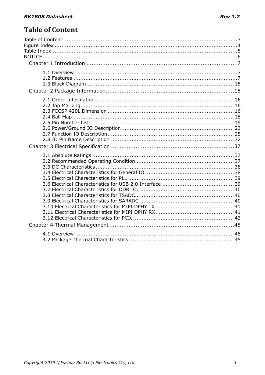
Table of Content
Table of Content ...................................................................................................... 3
Figure Index ........................................................................................................... 4
Table Index ............................................................................................................. 5
NOTICE .................................................................................................................. 6
Chapter 1 Introduction ..................................................................................... 7
1.1 Overview ............................................................................................... 7
1.2 Features ................................................................................................ 7
1.3 Block Diagram ...................................................................................... 15
Chapter 2 Package Information......................................................................... 16
2.1 Order Information ................................................................................. 16
2.2 Top Marking ......................................................................................... 16
2.3 FCCSP 420L Dimension .......................................................................... 16
2.4 Ball Map .............................................................................................. 18
2.5 Pin Number List .................................................................................... 19
2.6 Power/Ground IO Description .................................................................. 23
2.7 Function IO Description .......................................................................... 25
2.8 IO Pin Name Description ........................................................................ 32
Chapter 3 Electrical Specification ...................................................................... 37
3.1 Absolute Ratings ................................................................................... 37
3.2 Recommended Operating Condition ......................................................... 37
3.3 DC Characteristics ................................................................................. 38
3.4 Electrical Characteristics for General IO .................................................... 38
3.5 Electrical Characteristics for PLL .............................................................. 39
3.6 Electrical Characteristics for USB 2.0 Interface .......................................... 39
3.7 Electrical Characteristics for DDR IO......................................................... 40
3.8 Electrical Characteristics for TSADC.......................................................... 40
3.9 Electrical Characteristics for SARADC ....................................................... 40
3.10 Electrical Characteristics for MIPI DPHY TX .............................................. 41
3.11 Electrical Characteristics for MIPI DPHY RX .............................................. 41
3.12 Electrical Characteristics for PCIe ........................................................... 42
Chapter 4 Thermal Management ....................................................................... 45
4.1 Overview ............................................................................................. 45
4.2 Package Thermal Characteristics ............................................................. 45
Copyright 2019 ©Fuzhou Rockchip Electronics Co., Ltd. 3
�
RK1808 Datasheet Rev 1.2
Figure Index
Fig.1-1 Block Diagram .............................................................................................. 15
Fig.2-1 Package definition .................................................................................... 16
Fig.2-2 Package Top And Side View ....................................................................... 16
Fig.2-3 Package Bottom View ............................................................................... 17
Fig.2-4 Ball Map ................................................................................................. 18
Copyright 2019 ©Fuzhou Rockchip Electronics Co., Ltd. 4
�
RK1808 Datasheet Rev 1.2
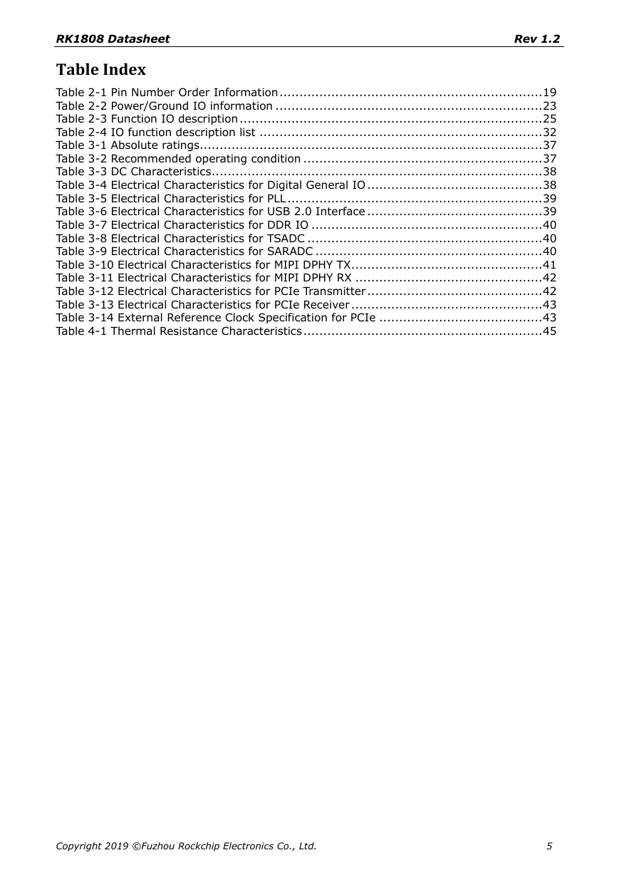
Table Index
Table 2-1 Pin Number Order Information .................................................................. 19
Table 2-2 Power/Ground IO information ................................................................... 23
Table 2-3 Function IO description ............................................................................ 25
Table 2-4 IO function description list ....................................................................... 32
Table 3-1 Absolute ratings...................................................................................... 37
Table 3-2 Recommended operating condition ............................................................ 37
Table 3-3 DC Characteristics ................................................................................... 38
Table 3-4 Electrical Characteristics for Digital General IO ............................................ 38
Table 3-5 Electrical Characteristics for PLL ................................................................ 39
Table 3-6 Electrical Characteristics for USB 2.0 Interface ............................................ 39
Table 3-7 Electrical Characteristics for DDR IO .......................................................... 40
Table 3-8 Electrical Characteristics for TSADC ........................................................... 40
Table 3-9 Electrical Characteristics for SARADC ......................................................... 40
Table 3-10 Electrical Characteristics for MIPI DPHY TX ................................................ 41
Table 3-11 Electrical Characteristics for MIPI DPHY RX ............................................... 42
Table 3-12 Electrical Characteristics for PCIe Transmitter ............................................ 42
Table 3-13 Electrical Characteristics for PCIe Receiver ................................................ 43
Table 3-14 External Reference Clock Specification for PCIe ......................................... 43
Table 4-1 Thermal Resistance Characteristics ............................................................ 45
Copyright 2019 ©Fuzhou Rockchip Electronics Co., Ltd. 5
�
RK1808 Datasheet Rev 1.2
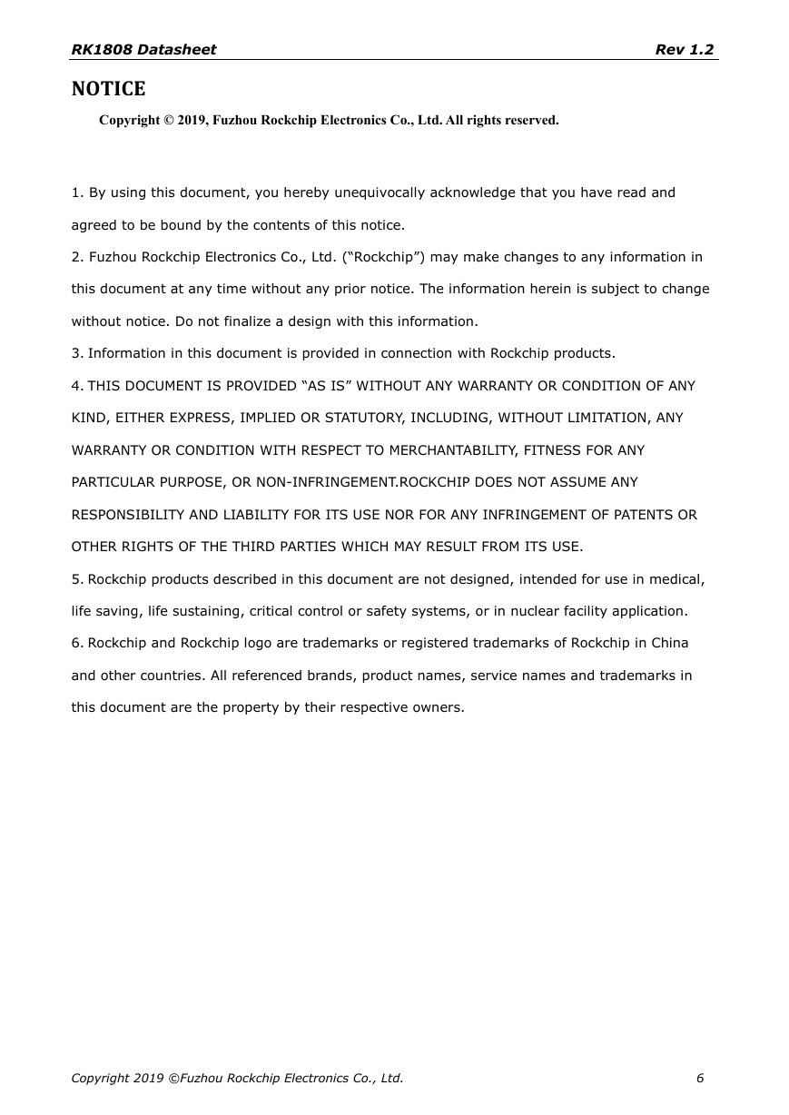
NOTICE
Copyright © 2019, Fuzhou Rockchip Electronics Co., Ltd. All rights reserved.
1. By using this document, you hereby unequivocally acknowledge that you have read and
agreed to be bound by the contents of this notice.
2. Fuzhou Rockchip Electronics Co., Ltd. (“Rockchip”) may make changes to any information in
this document at any time without any prior notice. The information herein is subject to change
without notice. Do not finalize a design with this information.
3. Information in this document is provided in connection with Rockchip products.
4. THIS DOCUMENT IS PROVIDED “AS IS” WITHOUT ANY WARRANTY OR CONDITION OF ANY
KIND, EITHER EXPRESS, IMPLIED OR STATUTORY, INCLUDING, WITHOUT LIMITATION, ANY
WARRANTY OR CONDITION WITH RESPECT TO MERCHANTABILITY, FITNESS FOR ANY
PARTICULAR PURPOSE, OR NON-INFRINGEMENT.ROCKCHIP DOES NOT ASSUME ANY
RESPONSIBILITY AND LIABILITY FOR ITS USE NOR FOR ANY INFRINGEMENT OF PATENTS OR
OTHER RIGHTS OF THE THIRD PARTIES WHICH MAY RESULT FROM ITS USE.
5. Rockchip products described in this document are not designed, intended for use in medical,
life saving, life sustaining, critical control or safety systems, or in nuclear facility application.
6. Rockchip and Rockchip logo are trademarks or registered trademarks of Rockchip in China
and other countries. All referenced brands, product names, service names and trademarks in
this document are the property by their respective owners.
Copyright 2019 ©Fuzhou Rockchip Electronics Co., Ltd. 6
�
RK1808 Datasheet Rev 1.2
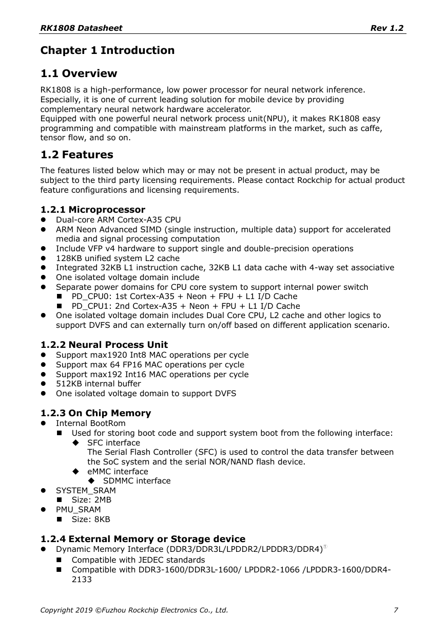
Chapter 1 Introduction
1.1 Overview
RK1808 is a high-performance, low power processor for neural network inference.
Especially, it is one of current leading solution for mobile device by providing
complementary neural network hardware accelerator.
Equipped with one powerful neural network process unit(NPU), it makes RK1808 easy
programming and compatible with mainstream platforms in the market, such as caffe,
tensor flow, and so on.
1.2 Features
The features listed below which may or may not be present in actual product, may be
subject to the third party licensing requirements. Please contact Rockchip for actual product
feature configurations and licensing requirements.
1.2.1 Microprocessor
Dual-core ARM Cortex-A35 CPU
ARM Neon Advanced SIMD (single instruction, multiple data) support for accelerated
media and signal processing computation
Include VFP v4 hardware to support single and double-precision operations
128KB unified system L2 cache
One isolated voltage domain include
Separate power domains for CPU core system to support internal power switch
Integrated 32KB L1 instruction cache, 32KB L1 data cache with 4-way set associative
PD_CPU0: 1st Cortex-A35 + Neon + FPU + L1 I/D Cache
PD_CPU1: 2nd Cortex-A35 + Neon + FPU + L1 I/D Cache
One isolated voltage domain includes Dual Core CPU, L2 cache and other logics to
support DVFS and can externally turn on/off based on different application scenario.
1.2.2 Neural Process Unit
Support max1920 Int8 MAC operations per cycle
Support max 64 FP16 MAC operations per cycle
Support max192 Int16 MAC operations per cycle
512KB internal buffer
One isolated voltage domain to support DVFS
1.2.3 On Chip Memory
Internal BootRom
Used for storing boot code and support system boot from the following interface:
SFC interface
The Serial Flash Controller (SFC) is used to control the data transfer between
the SoC system and the serial NOR/NAND flash device.
eMMC interface
SDMMC interface
SYSTEM_SRAM
Size: 2MB
PMU_SRAM
Size: 8KB
1.2.4 External Memory or Storage device
Dynamic Memory Interface (DDR3/DDR3L/LPDDR2/LPDDR3/DDR4)①
Compatible with JEDEC standards
Compatible with DDR3-1600/DDR3L-1600/ LPDDR2-1066 /LPDDR3-1600/DDR4-
2133
Copyright 2019 ©Fuzhou Rockchip Electronics Co., Ltd. 7
�
RK1808 Datasheet Rev 1.2
Support 32-bit data width, 2 ranks (chip selects), max 4GB addressing space per
rank, total addressing space is 4GB(max)
eMMC interface
Compatible with eMMC specification 4.41, 4.51
Support data bus width: 1-bit, 4-bit or 8-bit
Support up to max 150MB/s data transfer rates
SD/MMC interface
Compatible with SD3.0, MMC ver4.51
Data bus width is 4bits
Serial FLASH interface
Support x1,x2,x4 data bits mode
Support 1 chip select
1.2.5 System Component
CRU (clock & reset unit)
One oscillator with 24MHz clock input
Provide clock gating control for individual components
Support global soft-reset control for whole chip, also individual soft-reset for each
component.
PMU(Power Management Unit)
Manage on operating on 4 separate voltage domains for the digital logic circuit:
VD_CORE/VD_LOGIC/VD_NPU/VD_PMU
Provide powering up/down function for 7 power domains, which are included in the
4 voltage domains independently, to save power.
PD_CPU0 and PD_CPU1 in VD_CORE
PD_VIO, PD_PCIe, PD_VPU and PD_DDR in VD_LOGIC
Timer
Support 6 64-bit timers for non-secure application
Support 2 64-bit timers for secure application
Support two operation modes: free-running and user-defined count
PWM
Support 11 on-chip PWMs(PWM0~PWM3,PWM5~PWM11)
Embedded 32-bit timer/counter facility
Support capture mode
Support continuous mode or one-shot mode
Optimized for IR receiving application for PWM3, PWM7 and PWM11
Watchdog
One Watchdog for non-secure application
One Watchdog for secure application
32-bit watchdog counter
Counter counts down from a preset value to 0 to indicate the occurrence of a
timeout
WDT can perform two types of operations when timeout occurs:
Generate a system reset
First generate an interrupt and if this is not cleared by the service routine by
the time a second timeout occurs then generate a system reset
Totally 16 defined-ranges of main timeout period
Interrupt Controller
Support 256 SPI (Shared Peripheral Interrupts) interrupt sources input from
different components
Support 16 software-triggered interrupts
Two interrupt outputs (nFIQ and nIRQ) separately for each Cortex-A35, both are
low-level sensitive
Copyright 2019 ©Fuzhou Rockchip Electronics Co., Ltd. 8
�





 2023年江西萍乡中考道德与法治真题及答案.doc
 2012年重庆南川中考生物真题及答案.doc
 2013年江西师范大学地理学综合及文艺理论基础考研真题.doc
 2020年四川甘孜小升初语文真题及答案I卷.doc
 2020年注册岩土工程师专业基础考试真题及答案.doc
 2023-2024学年福建省厦门市九年级上学期数学月考试题及答案.doc
 2021-2022学年辽宁省沈阳市大东区九年级上学期语文期末试题及答案.doc
 2022-2023学年北京东城区初三第一学期物理期末试卷及答案.doc
 2018上半年江西教师资格初中地理学科知识与教学能力真题及答案.doc
 2012年河北国家公务员申论考试真题及答案-省级.doc
 2020-2021学年江苏省扬州市江都区邵樊片九年级上学期数学第一次质量检测试题及答案.doc
 2022下半年黑龙江教师资格证中学综合素质真题及答案.doc