Switch Connection Between Two Ports
D 5-W
D TTL-Compatible Input Levels
D Designed to Be Used in Level-Shifting
Applications
D Package Options Include Plastic
Small-Outline (DW), Shrink Small-Outline
(DB, DBQ), Thin Very Small-Outline (DGV),
and Thin Shrink Small-Outline (PW)
Packages, Ceramic Flat (W) Package,
Ceramic DIPs (JT), and Ceramic Chip
Carriers (FK)
description
The ’CBTD3384 devices provide ten bits of
high-speed TTL-compatible bus switching. The
low on-state resistance of the switches allows
connections
to be made without adding
propagation delay. A diode to VCC is integrated on
the die to allow for level shifting between 5-V
inputs and 3.3-V outputs.
These devices are organized as two 5-bit
switches with separate output-enable (OE)
inputs. When OE is low, the switch is on, and
port A is connected to port B. When OE is high, the
switch is open, and a high-impedance state exists
between the two ports.
The SN54CBTD3384
for
operation over the full military temperature range
from –55°C to 125°C. The SN74CBTD3384 is
characterized for operation from –40°C to 85°C.
is characterized
SN54CBTD3384, SN74CBTD3384
10-BIT FET BUS SWITCHES
WITH LEVEL SHIFTING
SCDS025L – MAY 1995 – REVISED MAY 2000
SN54CBTD3384 . . . JT OR W PACKAGE
SN74CBTD3384 . . . DB, DBQ, DGV, DW, OR PW PACKAGE
(TOP VIEW)
1OE
1B1
1A1
1A2
1B2
1B3
1A3
1A4
1B4
1B5
1A5
GND
1
2
3
4
5
6
7
8
9
10
11
12
24
23
22
21
20
19
18
17
16
15
14
13
VCC
2B5
2A5
2A4
2B4
2B3
2A3
2A2
2B2
2B1
2A1
2OE
SN54CBTD3384 . . . FK PACKAGE
(TOP VIEW)
1
A
1
1
B
1
E
O
1
C
C
V
C
N
5
B
2
5
A
2
1A2
1B2
1B3
NC
1A3
1A4
1B4
25
24
23
22
21
20
19
2A4
2B4
2B3
NC
2A3
2A2
2B2
3 2 1
28 27 26
4
5
6
7
8
9
10
11
12
13 14
15 16 17 18
5
B
1
5
A
1
D
N
G
C
N
E
O
2
1
A
2
1
B
2
NC – No internal connection
FUNCTION TABLE
(each 5-bit bus switch)
INPUTS
INPUTS/OUTPUTS
1OE
2OE
L
L
H
H
L
H
L
H
1B1–1B5
1A1–1A5
1A1–1A5
Z
Z
2B1–2B5
2A1–2A5
Z
2A1–2A5
Z
Please be aware that an important notice concerning availability, standard warranty, and use in critical applications of
Texas Instruments semiconductor products and disclaimers thereto appears at the end of this data sheet.
PRODUCTION DATA information is current as of publication date.
Products conform to specifications per the terms of Texas Instruments
standard warranty. Production processing does not necessarily include
testing of all parameters.
Copyright 2000, Texas Instruments Incorporated
On products compliant to MIL-PRF-38535, all parameters are tested
unless otherwise noted. On all other products, production
processing does not necessarily include testing of all parameters.
POST OFFICE BOX 655303 • DALLAS, TEXAS 75265
1
�
SN54CBTD3384, SN74CBTD3384
10-BIT FET BUS SWITCHES
WITH LEVEL SHIFTING
SCDS025L – MAY 1995 – REVISED MAY 2000
logic diagram (positive logic)
3
11
1
14
22
13
1A1
1A5
1OE
2A1
2A5
2OE
2
10
15
23
1B1
1B5
2B1
2B5
Pin numbers shown are for the DB, DBQ, DGV, DW, JT, PW, and W packages.
absolute maximum ratings over operating free-air temperature range (unless otherwise noted)†
. . . . . . . . . . . . . . . . . . . . . . . . . . . . . . . . . . . . . . . . . . . . . . . . . . . . . . . . . .
. . . . . . . . . . . . . . . . . . . . . . . . . . . . . . . . . . . . . . . . . . . . . . . . . .
Supply voltage range, VCC
Input voltage range, VI (see Note 1)
Continuous channel current
Input clamp current, IIK (VI/O < 0)
Package thermal impedance, q JA (see Note 2): DB package
DBQ package
DGV package
DW package
PW package
–0.5 V to 7 V
–0.5 V to 7 V
128 mA
–50 mA
63°C/W
61°C/W
86°C/W
46°C/W
88°C/W
–65°C to 150°C
† Stresses beyond those listed under “absolute maximum ratings” may cause permanent damage to the device. These are stress ratings only, and
functional operation of the device at these or any other conditions beyond those indicated under “recommended operating conditions” is not
implied. Exposure to absolute-maximum-rated conditions for extended periods may affect device reliability.
. . . . . . . . . . . . . . . . . . . . . . . . . . . . . . . . . . . . . . . . . . . . . . . . . . . . . . . . . . . . . .
. . . . . . . . . . . . . . . . . . . . . . . . . . . . . . . . . . . . . . . . . . . . . . . . . . . . . . . . .
. . . . . . . . . . . . . . . . . . . . . . . . . . . . . . . . .
. . . . . . . . . . . . . . . . . . . . . . . . . . . . . . . .
. . . . . . . . . . . . . . . . . . . . . . . . . . . . . . . .
. . . . . . . . . . . . . . . . . . . . . . . . . . . . . . . . .
. . . . . . . . . . . . . . . . . . . . . . . . . . . . . . . . .
Storage temperature range, Tstg
. . . . . . . . . . . . . . . . . . . . . . . . . . . . . . . . . . . . . . . . . . . . . . . . . . .
NOTES: 1. The input and output negative-voltage ratings may be exceeded if the input and output clamp-current ratings are observed.
2. The package thermal impedance is calculated in accordance with JESD 51.
recommended operating conditions (see Note 3)
VCC
VIH
VIL
TA
Supply voltage
High-level control input voltage
Low-level control input voltage
Operating free-air temperature
SN54CBTD3384 SN74CBTD3384
MAX
5.5
MAX
5.5
MIN
4.5
2
MIN
4.5
2
0.8
125
–55
0.8
85
–40
UNIT
UNIT
V
V
V
°C
NOTE 3: All unused control inputs of the device must be held at VCC or GND to ensure proper device operation. Refer to the TI application report,
Implications of Slow or Floating CMOS Inputs, literature number SCBA004.
2
POST OFFICE BOX 655303 • DALLAS, TEXAS 75265
�
SN54CBTD3384, SN74CBTD3384
10-BIT FET BUS SWITCHES
WITH LEVEL SHIFTING
SCDS025L – MAY 1995 – REVISED MAY 2000
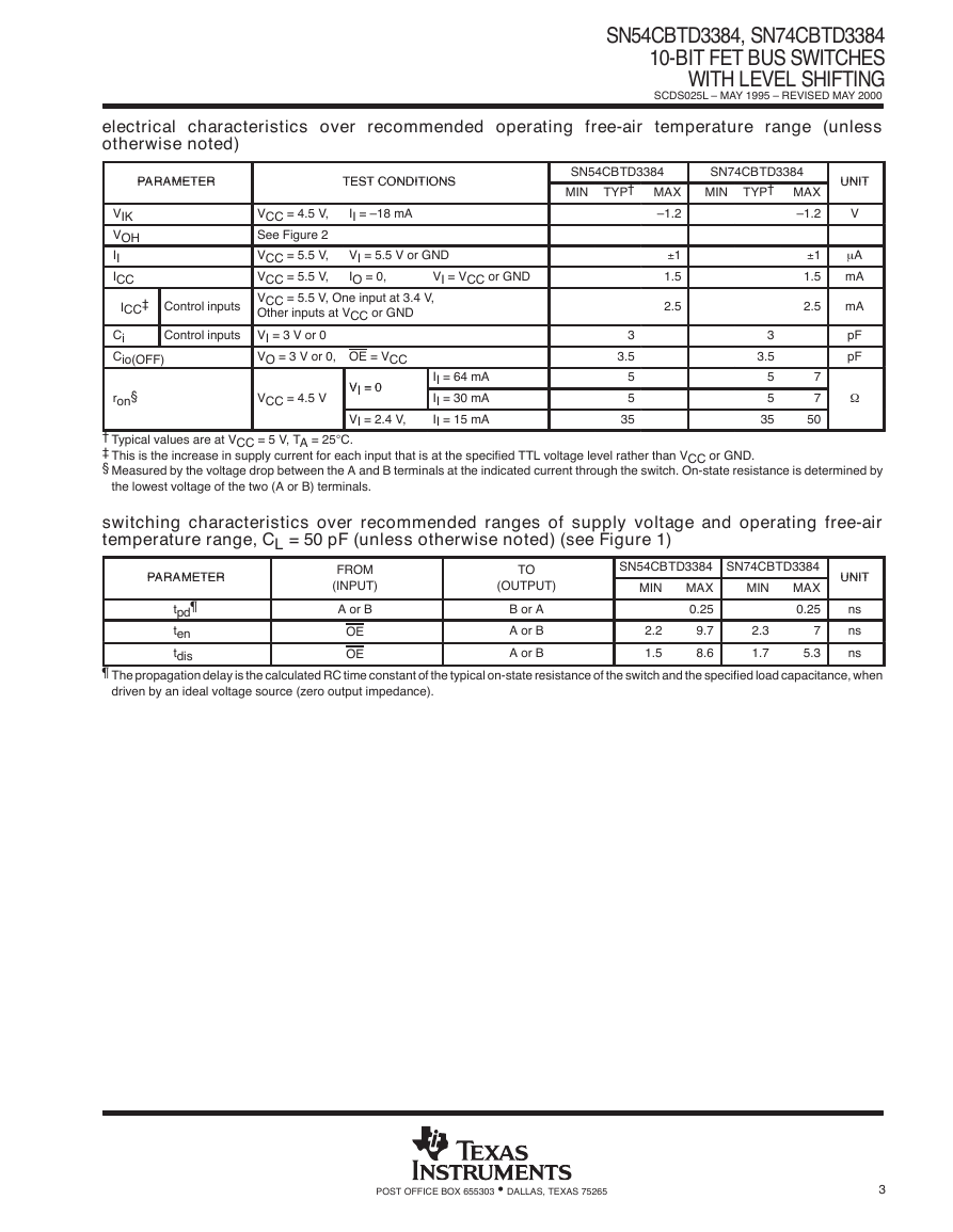
electrical characteristics over recommended operating free-air temperature range (unless
otherwise noted)
PARAMETER
PARAMETER
TEST CONDITIONS
TEST CONDITIONS
VIK
VOH
II
ICC
ICC‡ Control inputs
II = –18 mA
VCC = 4.5 V,
See Figure 2
VCC = 5.5 V,
VCC = 5.5 V,
VCC = 5.5 V, One input at 3.4 V,
Other inputs at VCC or GND
VI = 5.5 V or GND
IO = 0,
VI = VCC or GND
Control inputs VI = 3 V or 0
Ci
Cio(OFF)
§
ron§
SN54CBTD3384
MIN TYP† MAX
–1.2
SN74CBTD3384
MIN TYP† MAX
–1.2
±1
1.5
2.5
3
3.5
5
5
35
±1
1.5
2.5
7
7
50
3
3.5
5
5
35
UNIT
UNIT
V
m A
mA
mA
pF
pF
VO = 3 V or 0, OE = VCC
VCC = 4.5 V
VI = 0
VI = 0
VI = 2.4 V,
II = 64 mA
II = 30 mA
II = 15 mA
† Typical values are at VCC = 5 V, TA = 25°C.
‡ This is the increase in supply current for each input that is at the specified TTL voltage level rather than VCC or GND.
§ Measured by the voltage drop between the A and B terminals at the indicated current through the switch. On-state resistance is determined by
the lowest voltage of the two (A or B) terminals.
switching characteristics over recommended ranges of supply voltage and operating free-air
temperature range, CL = 50 pF (unless otherwise noted) (see Figure 1)
PARAMETER
PARAMETER
tpd¶
ten
tdis
FROM
(INPUT)
A or B
OE
OE
TO
(OUTPUT)
B or A
A or B
A or B
SN54CBTD3384 SN74CBTD3384
MAX
0.25
MAX
0.25
MIN
MIN
2.2
1.5
9.7
8.6
2.3
1.7
7
5.3
UNIT
UNIT
ns
ns
ns
¶ The propagation delay is the calculated RC time constant of the typical on-state resistance of the switch and the specified load capacitance, when
driven by an ideal voltage source (zero output impedance).
POST OFFICE BOX 655303 • DALLAS, TEXAS 75265
3
D
W
�
SN54CBTD3384, SN74CBTD3384
10-BIT FET BUS SWITCHES
WITH LEVEL SHIFTING
SCDS025L – MAY 1995 – REVISED MAY 2000
PARAMETER MEASUREMENT INFORMATION
From Output
Under Test
CL = 50 pF
(see Note A)
500 W
S1
7 V
Open
GND
500 W
TEST
tpd
tPLZ/tPZL
tPHZ/tPZH
S1
Open
7 V
Open
LOAD CIRCUIT
Input
1.5 V
1.5 V
Output
tPLH
1.5 V
3 V
0 V
VOH
VOL
tPHL
1.5 V
Output
Control
(low-level
enabling)
Output
Waveform 1
S1 at 7 V
(see Note B)
Output
Waveform 2
S1 at Open
(see Note B)
tPZL
tPZH
1.5 V
1.5 V
tPLZ
1.5 V
VOL + 0.3 V
3 V
0 V
3.5 V
VOL
1.5 V
tPHZ
VOH
VOH – 0.3 V
0 V
VOLTAGE WAVEFORMS
PROPAGATION DELAY TIMES
VOLTAGE WAVEFORMS
ENABLE AND DISABLE TIMES
NOTES: A. CL includes probe and jig capacitance.
B. Waveform 1 is for an output with internal conditions such that the output is low except when disabled by the output control.
Waveform 2 is for an output with internal conditions such that the output is high except when disabled by the output control.
C. All input pulses are supplied by generators having the following characteristics: PRR ≤ 10 MHz, ZO = 50 W
D. The outputs are measured one at a time with one transition per measurement.
E.
F.
G.
tPLZ and tPHZ are the same as tdis.
tPZL and tPZH are the same as ten.
tPLH and tPHL are the same as tpd.
, tr ≤ 2.5 ns, tf ≤ 2.5 ns.
Figure 1. Load Circuit and Voltage Waveforms
4
POST OFFICE BOX 655303 • DALLAS, TEXAS 75265
�
SN54CBTD3384, SN74CBTD3384
10-BIT FET BUS SWITCHES
WITH LEVEL SHIFTING
SCDS025L – MAY 1995 – REVISED MAY 2000
TYPICAL CHARACTERISTICS
OUTPUT VOLTAGE HIGH
vs
SUPPLY VOLTAGE
TA = 85°C
100 m A
6 mA
12 mA
24 mA
4
3.75
3.5
3.25
3
2.75
2.5
2.25
2
1.75
1.5
4.5
4.75
5
5.25
5.5
5.75
VCC – Supply Voltage – V
i
V
–
h
g
H
e
g
a
t
l
o
V
t
u
p
t
u
O
–
H
O
V
OUTPUT VOLTAGE HIGH
vs
SUPPLY VOLTAGE
TA = 25°C
100 m A
6 mA
12 mA
24 mA
4.75
5
5.25
5.5
5.75
VCC – Supply Voltage – V
4
3.75
3.5
3.25
3
2.75
2.5
2.25
2
1.75
1.5
4.5
i
V
–
h
g
H
e
g
a
t
l
o
V
t
u
p
t
u
O
–
H
O
V
i
V
–
h
g
H
e
g
a
t
l
o
V
t
u
p
t
u
O
–
H
O
V
4
3.75
3.5
3.25
3
2.75
2.5
2.25
2
1.75
1.5
4.5
OUTPUT VOLTAGE HIGH
vs
SUPPLY VOLTAGE
TA = 0°C
100 m A
6 mA
12 mA
24 mA
4.75
5
5.25
5.5
5.75
VCC – Supply Voltage – V
Figure 2. VOH Values
POST OFFICE BOX 655303 • DALLAS, TEXAS 75265
5
�
IMPORTANT NOTICE
Texas Instruments and its subsidiaries (TI) reserve the right to make changes to their products or to discontinue
any product or service without notice, and advise customers to obtain the latest version of relevant information
to verify, before placing orders, that information being relied on is current and complete. All products are sold
subject to the terms and conditions of sale supplied at the time of order acknowledgment, including those
pertaining to warranty, patent infringement, and limitation of liability.
TI warrants performance of its semiconductor products to the specifications applicable at the time of sale in
accordance with TI’s standard warranty. Testing and other quality control techniques are utilized to the extent
TI deems necessary to support this warranty. Specific testing of all parameters of each device is not necessarily
performed, except those mandated by government requirements.
Customers are responsible for their applications using TI components.
In order to minimize risks associated with the customer’s applications, adequate design and operating
safeguards must be provided by the customer to minimize inherent or procedural hazards.
TI assumes no liability for applications assistance or customer product design. TI does not warrant or represent
that any license, either express or implied, is granted under any patent right, copyright, mask work right, or other
intellectual property right of TI covering or relating to any combination, machine, or process in which such
semiconductor products or services might be or are used. TI’s publication of information regarding any third
party’s products or services does not constitute TI’s approval, warranty or endorsement thereof.
Copyright 2000, Texas Instruments Incorporated
�


 2023年江西萍乡中考道德与法治真题及答案.doc
 2012年重庆南川中考生物真题及答案.doc
 2013年江西师范大学地理学综合及文艺理论基础考研真题.doc
 2020年四川甘孜小升初语文真题及答案I卷.doc
 2020年注册岩土工程师专业基础考试真题及答案.doc
 2023-2024学年福建省厦门市九年级上学期数学月考试题及答案.doc
 2021-2022学年辽宁省沈阳市大东区九年级上学期语文期末试题及答案.doc
 2022-2023学年北京东城区初三第一学期物理期末试卷及答案.doc
 2018上半年江西教师资格初中地理学科知识与教学能力真题及答案.doc
 2012年河北国家公务员申论考试真题及答案-省级.doc
 2020-2021学年江苏省扬州市江都区邵樊片九年级上学期数学第一次质量检测试题及答案.doc
 2022下半年黑龙江教师资格证中学综合素质真题及答案.doc