查询AT89C51供应商
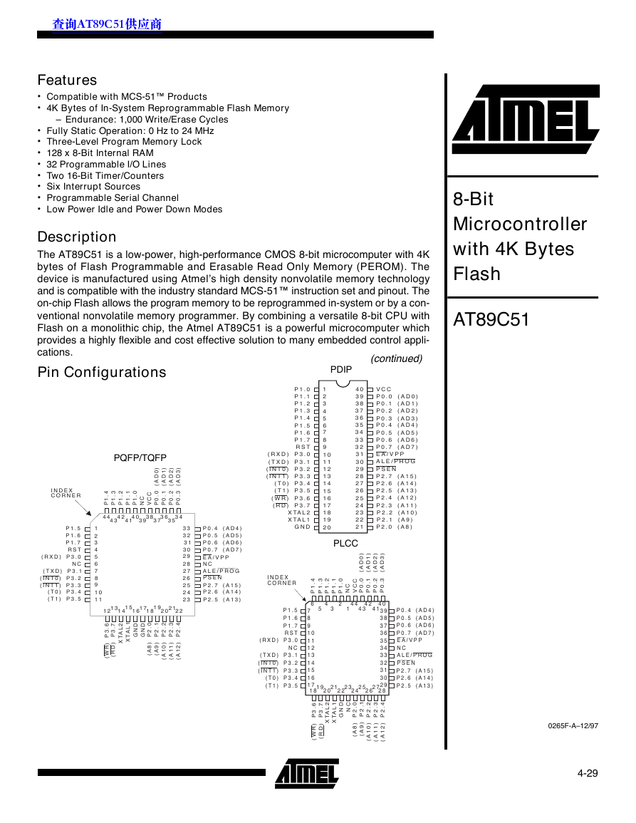
4-29PQFP/TQFP231INDEXCORNER34P1.0VCCP1.1P1.2P1.4P1.3NC42434041654443226252827241819202122P1.7P1.6P1.5NC789101112131415161729303938373635333231NCPSENXTAL1GNDXTAL2GNDP0.0(AD0)ALE/PROG()P3.7RDEA/VPP()P3.6WR(RXD)P3.0P0.7(AD7)P2.6(A14)P0.6(AD6)P0.5(AD5)P0.4(AD4)P0.3(AD3)P0.2(AD2)P0.1(AD1)()P3.2INT0(TXD)P3.1(T1)P3.5()P3.3INT1(T0)P3.4P2.7(A15)(A11)P2.3(A12)P2.4(A10)P2.2(A9)P2.1(A8)P2.0RSTP2.5(A13)Features•Compatible with MCS-51™ Products•4K Bytes of In-System Reprogrammable Flash Memory–Endurance: 1,000 Write/Erase Cycles•Fully Static Operation: 0 Hz to 24 MHz•Three-Level Program Memory Lock•128 x 8-Bit Internal RAM•32 Programmable I/O Lines•Two 16-Bit Timer/Counters•Six Interrupt Sources•Programmable Serial Channel•Low Power Idle and Power Down ModesDescriptionThe AT89C51 is a low-power, high-performance CMOS 8-bit microcomputer with 4Kbytes of Flash Programmable and Erasable Read Only Memory (PEROM). Thedevice is manufactured using Atmel’s high density nonvolatile memory technologyand is compatible with the industry standard MCS-51™ instruction set and pinout. Theon-chip Flash allows the program memory to be reprogrammed in-system or by a con-ventional nonvolatile memory programmer. By combining a versatile 8-bit CPU withFlash on a monolithic chip, the Atmel AT89C51 is a powerful microcomputer whichprovides a highly flexible and cost effective solution to many embedded control appli-cations.PDIPP1.0VCCP1.1P0.0(AD0)P1.2()P3.2INT0ALE/PROG()P3.7RDP2.3(A11)(TXD)P3.1EA/VPP()P3.6WRP2.4(A12)(RXD)P3.0P0.7(AD7)(T1)P3.5P2.6(A14)RSTP0.6(AD6)P1.7P0.5(AD5)P1.6P0.4(AD4)P1.5P0.3(AD3)P1.4P0.2(AD2)P1.3P0.1(AD1)()P3.3INT1PSENXTAL2P2.2(A10)(T0)P3.4P2.7(A15)XTAL1P2.1(A9)GNDP2.0(A8)P2.5(A13)201918171615123456789101112131421222324252640393837363534333231302928270265F-A–12/97(continued)8-Bit Microcontroller with 4K Bytes FlashAT89C51Pin ConfigurationsPLCCP1.0VCCP1.1P0.0(AD0)P1.2ALE/PROG()P3.7RDXTAL1EA/VPP()P3.6WRGND(RXD)P3.0P0.7(AD7)P2.6(A14)P0.6(AD6)P0.5(AD5)P0.4(AD4)P0.3(AD3)P1.4P0.2(AD2)P1.3P0.1(AD1)PSENXTAL2()P3.2INT0(TXD)P3.1(T1)P3.5()P3.3INT1(T0)P3.4P2.7(A15)(A11)P2.3(A12)P2.4(A10)P2.2(A9)P2.1(A8)P2.0NC231RSTP1.7P1.6P1.5INDEXCORNERNCNCP2.5(A13)34NC42434041654443226252827181920242122789101112131415161729303938373635333231�
AT89C514-30Block DiagramPORT2DRIVERSPORT2LATCHP2.0-P2.7FLASHPORT0LATCHRAMPROGRAMADDRESSREGISTERBUFFERPCINCREMENTERPROGRAMCOUNTERDPTRRAMADDR.REGISTERINSTRUCTIONREGISTERBREGISTERINTERRUPT,SERIALPORT,ANDTIMERBLOCKSSTACKPOINTERACCTMP2TMP1ALUPSWTIMINGANDCONTROLPORT3LATCHPORT3DRIVERSP3.0-P3.7PORT1LATCHPORT1DRIVERSP1.0-P1.7OSCGNDVCCPSENALE/PROGEA/VPPRSTPORT0DRIVERSP0.0-P0.7�
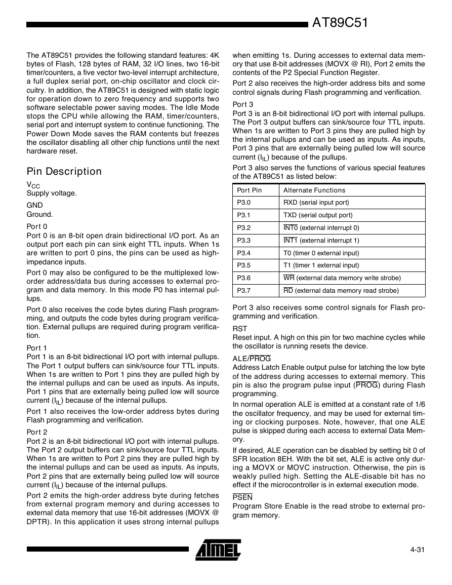
AT89C514-31The AT89C51 provides the following standard features: 4Kbytes of Flash, 128 bytes of RAM, 32 I/O lines, two 16-bittimer/counters, a five vector two-level interrupt architecture,a full duplex serial port, on-chip oscillator and clock cir-cuitry. In addition, the AT89C51 is designed with static logicfor operation down to zero frequency and supports twosoftware selectable power saving modes. The Idle Modestops the CPU while allowing the RAM, timer/counters,serial port and interrupt system to continue functioning. ThePower Down Mode saves the RAM contents but freezesthe oscillator disabling all other chip functions until the nexthardware reset.Pin DescriptionVCCSupply voltage.GNDGround.Port 0Port 0 is an 8-bit open drain bidirectional I/O port. As anoutput port each pin can sink eight TTL inputs. When 1sare written to port 0 pins, the pins can be used as high-impedance inputs. Port 0 may also be configured to be the multiplexed low-order address/data bus during accesses to external pro-gram and data memory. In this mode P0 has internal pul-lups.Port 0 also receives the code bytes during Flash program-ming, and outputs the code bytes during program verifica-tion. External pullups are required during program verifica-tion. Port 1Port 1 is an 8-bit bidirectional I/O port with internal pullups.The Port 1 output buffers can sink/source four TTL inputs.When 1s are written to Port 1 pins they are pulled high bythe internal pullups and can be used as inputs. As inputs,Port 1 pins that are externally being pulled low will sourcecurrent (IIL) because of the internal pullups. Port 1 also receives the low-order address bytes duringFlash programming and verification. Port 2Port 2 is an 8-bit bidirectional I/O port with internal pullups.The Port 2 output buffers can sink/source four TTL inputs.When 1s are written to Port 2 pins they are pulled high bythe internal pullups and can be used as inputs. As inputs,Port 2 pins that are externally being pulled low will sourcecurrent (IIL) because of the internal pullups. Port 2 emits the high-order address byte during fetchesfrom external program memory and during accesses toexternal data memory that use 16-bit addresses (MOVX @DPTR). In this application it uses strong internal pullupswhen emitting 1s. During accesses to external data mem-ory that use 8-bit addresses (MOVX @ RI), Port 2 emits thecontents of the P2 Special Function Register. Port 2 also receives the high-order address bits and somecontrol signals during Flash programming and verification.Port 3Port 3 is an 8-bit bidirectional I/O port with internal pullups.The Port 3 output buffers can sink/source four TTL inputs.When 1s are written to Port 3 pins they are pulled high bythe internal pullups and can be used as inputs. As inputs,Port 3 pins that are externally being pulled low will sourcecurrent (IIL) because of the pullups.Port 3 also serves the functions of various special featuresof the AT89C51 as listed below:Port 3 also receives some control signals for Flash pro-gramming and verification. RSTReset input. A high on this pin for two machine cycles whilethe oscillator is running resets the device. ALE/PROGAddress Latch Enable output pulse for latching the low byteof the address during accesses to external memory. Thispin is also the program pulse input (PROG) during Flashprogramming. In normal operation ALE is emitted at a constant rate of 1/6the oscillator frequency, and may be used for external tim-ing or clocking purposes. Note, however, that one ALEpulse is skipped during each access to external Data Mem-ory. If desired, ALE operation can be disabled by setting bit 0 ofSFR location 8EH. With the bit set, ALE is active only dur-ing a MOVX or MOVC instruction. Otherwise, the pin isweakly pulled high. Setting the ALE-disable bit has noeffect if the microcontroller is in external execution mode.PSENProgram Store Enable is the read strobe to external pro-gram memory. Port PinAlternate FunctionsP3.0RXD (serial input port)P3.1TXD (serial output port)P3.2INT0 (external interrupt 0)P3.3INT1 (external interrupt 1)P3.4T0 (timer 0 external input)P3.5T1 (timer 1 external input)P3.6WR (external data memory write strobe)P3.7RD (external data memory read strobe)�
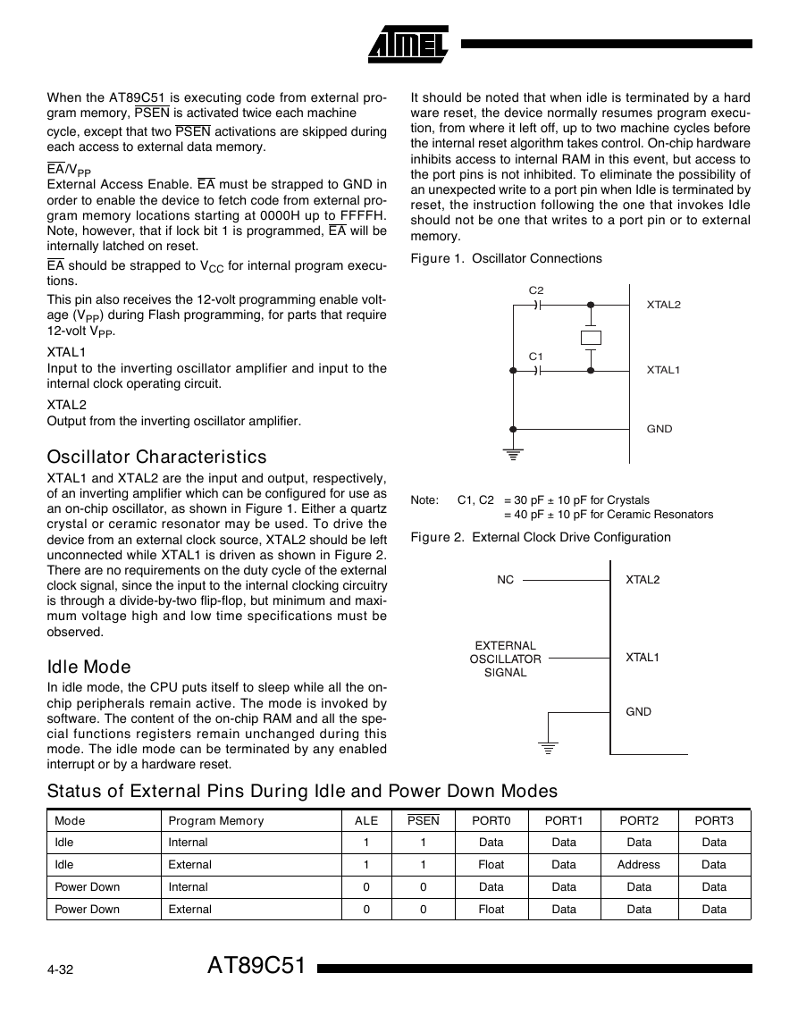
AT89C514-32When the AT89C51 is executing code from external pro-gram memory, PSEN is activated twice each machine cycle, except that two PSEN activations are skipped duringeach access to external data memory. EA/VPPExternal Access Enable. EA must be strapped to GND inorder to enable the device to fetch code from external pro-gram memory locations starting at 0000H up to FFFFH.Note, however, that if lock bit 1 is programmed, EA will beinternally latched on reset. EA should be strapped to VCC for internal program execu-tions.This pin also receives the 12-volt programming enable volt-age (VPP) during Flash programming, for parts that require12-volt VPP.XTAL1Input to the inverting oscillator amplifier and input to theinternal clock operating circuit. XTAL2Output from the inverting oscillator amplifier.Oscillator Characteristics XTAL1 and XTAL2 are the input and output, respectively,of an inverting amplifier which can be configured for use asan on-chip oscillator, as shown in Figure 1. Either a quartzcrystal or ceramic resonator may be used. To drive thedevice from an external clock source, XTAL2 should be leftunconnected while XTAL1 is driven as shown in Figure 2.There are no requirements on the duty cycle of the externalclock signal, since the input to the internal clocking circuitryis through a divide-by-two flip-flop, but minimum and maxi-mum voltage high and low time specifications must beobserved.Idle Mode In idle mode, the CPU puts itself to sleep while all the on-chip peripherals remain active. The mode is invoked bysoftware. The content of the on-chip RAM and all the spe-cial functions registers remain unchanged during thismode. The idle mode can be terminated by any enabledinterrupt or by a hardware reset. It should be noted that when idle is terminated by a hardware reset, the device normally resumes program execu-tion, from where it left off, up to two machine cycles beforethe internal reset algorithm takes control. On-chip hardwareinhibits access to internal RAM in this event, but access tothe port pins is not inhibited. To eliminate the possibility ofan unexpected write to a port pin when Idle is terminated byreset, the instruction following the one that invokes Idleshould not be one that writes to a port pin or to externalmemory.Figure 1. Oscillator ConnectionsNote:C1, C2 = 30 pF – 10 pF for Crystals= 40 pF – 10 pF for Ceramic ResonatorsFigure 2. External Clock Drive ConfigurationC2XTAL2GNDXTAL1C1Status of External Pins During Idle and Power Down ModesModeProgram MemoryALEPSENPORT0PORT1PORT2PORT3IdleInternal11DataDataDataDataIdleExternal11FloatDataAddressDataPower DownInternal00DataDataDataDataPower DownExternal00FloatDataDataData�
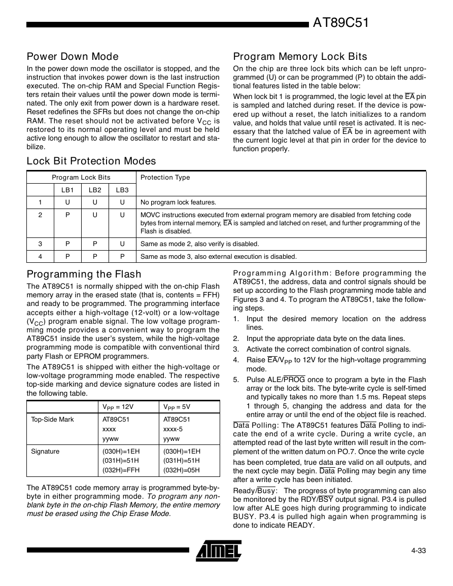
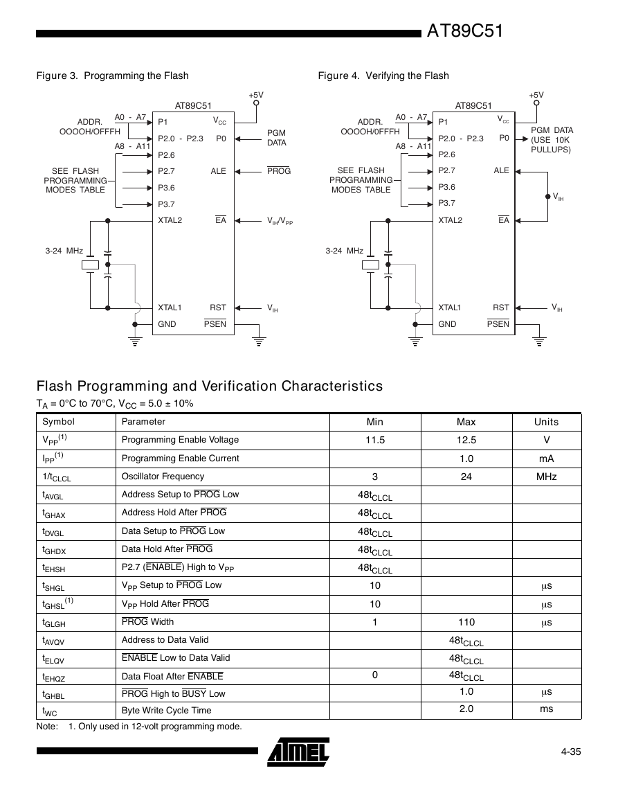
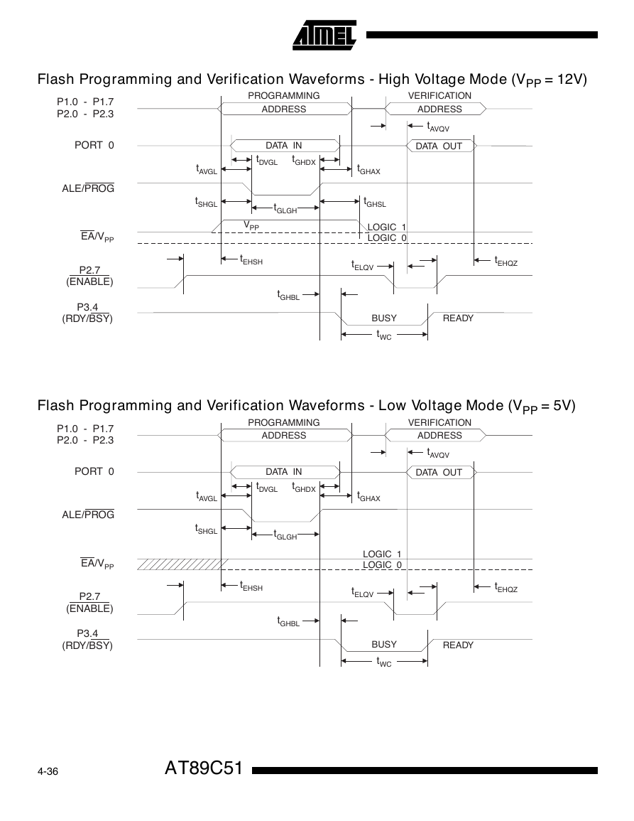
AT89C514-33Power Down Mode In the power down mode the oscillator is stopped, and theinstruction that invokes power down is the last instructionexecuted. The on-chip RAM and Special Function Regis-ters retain their values until the power down mode is termi-nated. The only exit from power down is a hardware reset.Reset redefines the SFRs but does not change the on-chipRAM. The reset should not be activated before VCC isrestored to its normal operating level and must be heldactive long enough to allow the oscillator to restart and sta-bilize.Program Memory Lock Bits On the chip are three lock bits which can be left unpro-grammed (U) or can be programmed (P) to obtain the addi-tional features listed in the table below:When lock bit 1 is programmed, the logic level at the EA pinis sampled and latched during reset. If the device is pow-ered up without a reset, the latch initializes to a randomvalue, and holds that value until reset is activated. It is nec-essary that the latched value of EA be in agreement withthe current logic level at that pin in order for the device tofunction properly.Lock Bit Protection ModesProgram Lock BitsProtection TypeLB1LB2LB31UUUNo program lock features.2PUUMOVC instructions executed from external program memory are disabled from fetching code bytes from internal memory, EA is sampled and latched on reset, and further programming of the Flash is disabled.3PPUSame as mode 2, also verify is disabled.4PPPSame as mode 3, also external execution is disabled.Programming the Flash The AT89C51 is normally shipped with the on-chip Flashmemory array in the erased state (that is, contents = FFH)and ready to be programmed. The programming interfaceaccepts either a high-voltage (12-volt) or a low-voltage(VCC) program enable signal. The low voltage program-ming mode provides a convenient way to program theAT89C51 inside the user’s system, while the high-voltageprogramming mode is compatible with conventional thirdparty Flash or EPROM programmers.The AT89C51 is shipped with either the high-voltage orlow-voltage programming mode enabled. The respectivetop-side marking and device signature codes are listed inthe following table.The AT89C51 code memory array is programmed byte-by-byte in either programming mode. To program any non-blank byte in the on-chip Flash Memory, the entire memorymust be erased using the Chip Erase Mode.Programming Algorithm: Before programming theAT89C51, the address, data and control signals should beset up according to the Flash programming mode table andFigures 3 and 4. To program the AT89C51, take the follow-ing steps.1.Input the desired memory location on the addresslines.2.Input the appropriate data byte on the data lines. 3.Activate the correct combination of control signals.4.Raise EA/VPP to 12V for the high-voltage programmingmode. 5.Pulse ALE/PROG once to program a byte in the Flasharray or the lock bits. The byte-write cycle is self-timedand typically takes no more than 1.5 ms. Repeat steps1 through 5, changing the address and data for theentire array or until the end of the object file is reached.Data Polling: The AT89C51 features Data Polling to indi-cate the end of a write cycle. During a write cycle, anattempted read of the last byte written will result in the com-plement of the written datum on PO.7. Once the write cycle has been completed, true data are valid on all outputs, andthe next cycle may begin. Data Polling may begin any timeafter a write cycle has been initiated. Ready/Busy: The progress of byte programming can alsobe monitored by the RDY/BSY output signal. P3.4 is pulledlow after ALE goes high during programming to indicateBUSY. P3.4 is pulled high again when programming isdone to indicate READY.VPP = 12VVPP = 5VTop-Side MarkAT89C51xxxxyywwAT89C51xxxx-5yywwSignature(030H)=1EH(031H)=51H(032H)=FFH(030H)=1EH(031H)=51H(032H)=05H�
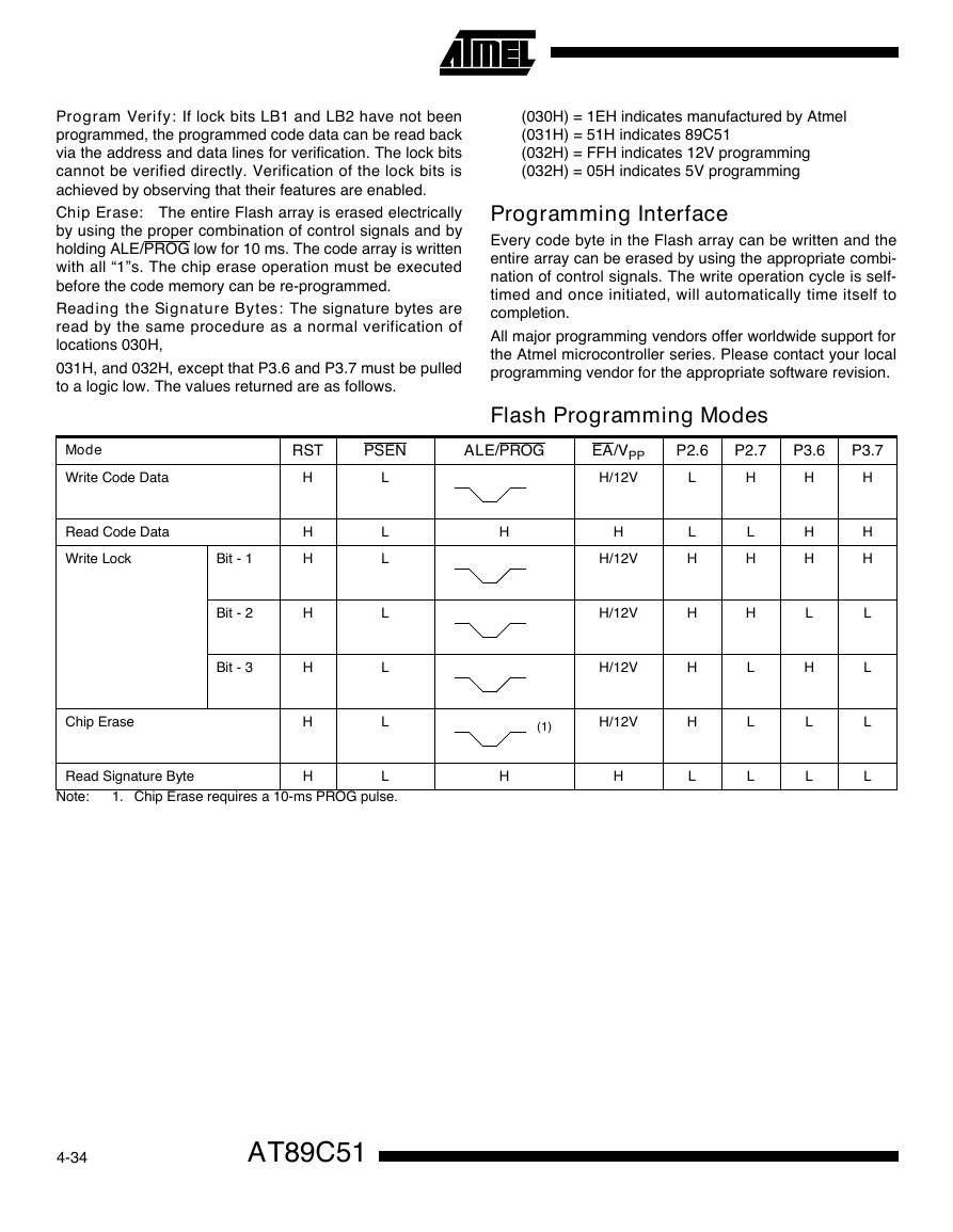
AT89C514-34Program Verify: If lock bits LB1 and LB2 have not beenprogrammed, the programmed code data can be read backvia the address and data lines for verification. The lock bitscannot be verified directly. Verification of the lock bits isachieved by observing that their features are enabled. Chip Erase: The entire Flash array is erased electricallyby using the proper combination of control signals and byholding ALE/PROG low for 10 ms. The code array is writtenwith all “1”s. The chip erase operation must be executedbefore the code memory can be re-programmed. Reading the Signature Bytes: The signature bytes areread by the same procedure as a normal verification oflocations 030H, 031H, and 032H, except that P3.6 and P3.7 must be pulledto a logic low. The values returned are as follows. (030H) = 1EH indicates manufactured by Atmel(031H) = 51H indicates 89C51(032H) = FFH indicates 12V programming(032H) = 05H indicates 5V programmingProgramming InterfaceEvery code byte in the Flash array can be written and theentire array can be erased by using the appropriate combi-nation of control signals. The write operation cycle is self-timed and once initiated, will automatically time itself tocompletion.All major programming vendors offer worldwide support forthe Atmel microcontroller series. Please contact your localprogramming vendor for the appropriate software revision.Flash Programming ModesNote:1.Chip Erase requires a 10-ms PROG pulse.ModeRSTPSENALE/PROGEA/VPPP2.6P2.7P3.6P3.7Write Code DataHL H/12VLHHHRead Code DataHLHHLLHHWrite LockBit - 1HLH/12VHHHHBit - 2HLH/12VHHLLBit - 3HLH/12VHLHLChip EraseHLH/12VHLLLRead Signature ByteHLHHLLLL(1)�
AT89C514-35Figure 3. Programming the FlashFigure 4. Verifying the FlashP1P2.6P3.6P2.0-P2.3A0-A7ADDR.OOOOH/OFFFHTSEEFLASHPROGRAMMINGMODESABLE3-24MHzA8-A11P0+5VP2.7PGMDATAPROGV/VIHPPVIHALEP3.7XTAL2EARSTPSENXTAL1GNDVCCAT89C51P1P2.6P3.6P2.0-P2.3A0-A7ADDR.OOOOH/0FFFH3-24MHzA8-A11P0+5VP2.7PGMDATA(USE10KPULLUPS)VIHVIHALEP3.7XTAL2EARSTPSENXTAL1GNDVCCAT89C51TSEEFLASHPROGRAMMINGMODESABLEFlash Programming and Verification Characteristics TA = 0°C to 70°C, VCC = 5.0 – 10%Note:1. Only used in 12-volt programming mode.SymbolParameterMinMaxUnitsVPP(1)Programming Enable Voltage11.512.5VIPP(1)Programming Enable Current1.0mA1/tCLCLOscillator Frequency324MHztAVGLAddress Setup to PROG Low48tCLCLtGHAXAddress Hold After PROG48tCLCLtDVGLData Setup to PROG Low48tCLCLtGHDXData Hold After PROG48tCLCLtEHSHP2.7 (ENABLE) High to VPP48tCLCLtSHGLVPP Setup to PROG Low10mstGHSL(1)VPP Hold After PROG10mstGLGHPROG Width1110mstAVQVAddress to Data Valid48tCLCLtELQVENABLE Low to Data Valid48tCLCLtEHQZData Float After ENABLE048tCLCLtGHBLPROG High to BUSY Low1.0mstWCByte Write Cycle Time2.0ms�
AT89C514-36Flash Programming and Verification Waveforms - High Voltage Mode (VPP = 12V)tGLGHtGHSLtAVGLtSHGLtDVGLtGHAXtAVQVtGHDXtEHSHtELQVtWCBUSYREADYtGHBLtEHQZP1.0-P1.7P2.0-P2.3ALE/PROGPORT0LOGIC1LOGIC0EA/VPPVPPP2.7(ENABLE)P3.4(RDY/BSY)PROGRAMMINGADDRESSVERIFICATIONADDRESSDATAINDATAOUTFlash Programming and Verification Waveforms - Low Voltage Mode (VPP = 5V)tGLGHtAVGLtSHGLtDVGLtGHAXtAVQVtGHDXtEHSHtELQVtWCBUSYREADYtGHBLtEHQZP1.0-P1.7P2.0-P2.3ALE/PROGPORT0LOGIC1LOGIC0EA/VPPP2.7(ENABLE)P3.4(RDY/BSY)PROGRAMMINGADDRESSVERIFICATIONADDRESSDATAINDATAOUT�



 2023年江西萍乡中考道德与法治真题及答案.doc
 2012年重庆南川中考生物真题及答案.doc
 2013年江西师范大学地理学综合及文艺理论基础考研真题.doc
 2020年四川甘孜小升初语文真题及答案I卷.doc
 2020年注册岩土工程师专业基础考试真题及答案.doc
 2023-2024学年福建省厦门市九年级上学期数学月考试题及答案.doc
 2021-2022学年辽宁省沈阳市大东区九年级上学期语文期末试题及答案.doc
 2022-2023学年北京东城区初三第一学期物理期末试卷及答案.doc
 2018上半年江西教师资格初中地理学科知识与教学能力真题及答案.doc
 2012年河北国家公务员申论考试真题及答案-省级.doc
 2020-2021学年江苏省扬州市江都区邵樊片九年级上学期数学第一次质量检测试题及答案.doc
 2022下半年黑龙江教师资格证中学综合素质真题及答案.doc