AT89C51 的概况
The General Situation of AT89C51
Chapter 1 The application of AT89C51
Microcontrollers are used in a multitude of commercial applications
such as modems, motor-control systems, air conditioner control systems,
automotive engine and among others. The high processing speed and enhanced
peripheral set of these microcontrollers make them suitable for such
high-speed event-based applications.
However, these critical
application domains also require that these microcontrollers are highly
reliable. The high reliability and low market risks can be ensured by a
robust testing process and a proper tools environment for the validation
of these microcontrollers both at the component and at the system level.
Intel Plaform Engineering department developed an object-oriented
multi-threaded test environment for the validation of its AT89C51
automotive microcontrollers. The goals of thisenvironment was not only
to provide a robust testing environment for the AT89C51 automotive
microcontrollers, but to develop an environment which can be easily
extended and reused for the validation of several other future
microcontrollers. The environment was developed in conjunction with
Microsoft Foundation Classes (AT89C51). The paper describes the design
and mechanism of this test environment, its interactions with various
hardware/software environmental components, and how to use AT89C51.
1.1 Introduction
The 8-bit AT89C51 CHMOS microcontrollers are designed to handle
high-speedcalculations
and
fast
input/output
operations.
MCS
51
microcontrollers are typically used for high-speed event control systems.
Commercial applications include modems,motor-control systems, printers,
photocopiers, air conditioner control systems, disk drives,and medical
instruments. The automotive industry use MCS 51 microcontrollers in
engine-control systems, airbags, suspension systems, and antilock
braking systems (ABS). The AT89C51 is especially well suited to
applications that benefit from its processing speed and enhanced on-chip
�
peripheral functions set, such as automotive power-train control, vehicle
dynamic suspension, antilock braking, and stability control applications.
Because of these critical applications, the market requires a reliable
cost-effective controller with a low interrupt latency response, ability
to service the high number of time and event driven integrated peripherals
needed in real time applications, and a CPU with above average processing
power in a single package. The financial and legal risk of having devices
that operate unpredictably is very high. Once in the market, particularly
in mission criticalapplications such as an autopilot or anti-lock braking
system, mistakes are financiallyprohibitive. Redesign costs can run as
high as a $500K, much more if the fix means 2 back annotating it across
a product family that share the same core and/or peripheral design flaw.
In addition, field replacements of components is extremely expensive, as
the devices are typically sealed in modules with a total value several
times that of the component. To mitigate these problems, it is essential
that comprehensive testing of the controllers be carried out at both the
component level and system level under worst case environmental and
voltage conditions.This complete and thorough validation necessitates
not only a well-defined process but also a proper environment and tools
to facilitate and execute the mission successfully.Intel Chandler
Platform Engineering group provides post silicon system validation (SV)
of various micro-controllers and processors. The system validation
process can be broken into three major parts.The type of the device and
its application requirements determine which types of testing are
performed on the device.
1.2 The AT89C51 provides the following standard features:
4Kbytes
of
Flash,
128
bytes
of
RAM,
32
I/O
lines,
two
16-bittimer/counters, a five vector two-level interrupt architecture,a
full duple ser -ial port, on-chip oscillator and clock circuitry.In
addition, the AT89C51 is designed with static logic for operation down
to zero frequency and supports two software selectable power saving modes.
The Idle Mode stops the CPU while allowing the RAM, timer/counters,serial
port and interrupt sys -tem to continue functioning. The Power-down Mode
saves the RAM contents but freezes the oscil –lator disabling all other
�
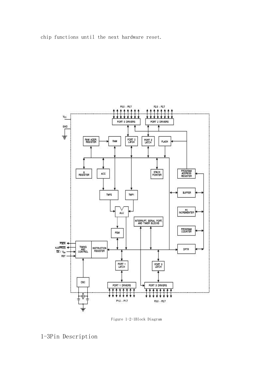
chip functions until the next hardware reset.
Figure 1-2-1Block Diagram
1-3Pin Description
�
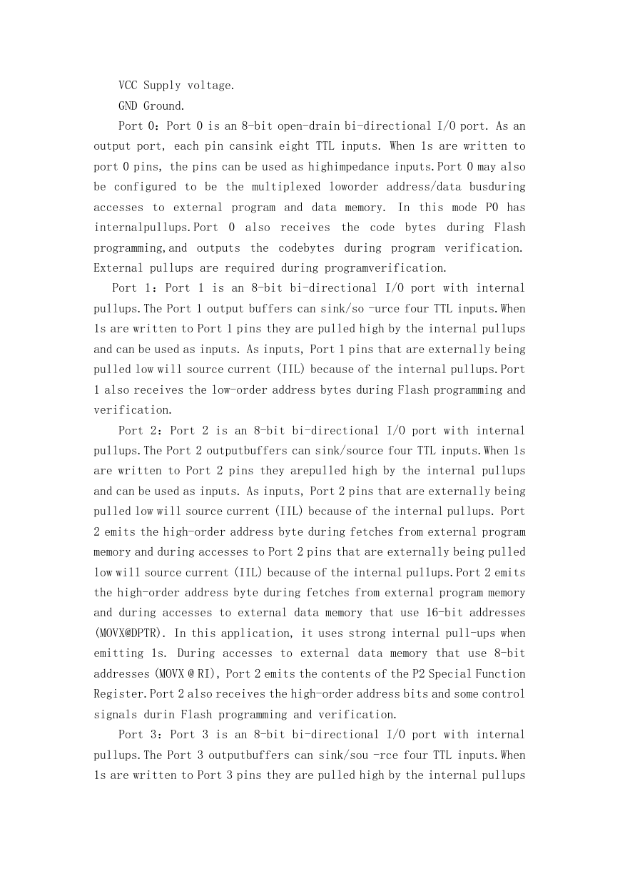
VCC Supply voltage.
GND Ground.
Port 0:Port 0 is an 8-bit open-drain bi-directional I/O port. As an
output port, each pin cansink eight TTL inputs. When 1s are written to
port 0 pins, the pins can be used as highimpedance inputs.Port 0 may also
be configured to be the multiplexed loworder address/data busduring
accesses to external program and data memory. In this mode P0 has
internalpullups.Port 0 also receives the code bytes during Flash
programming,and outputs the codebytes during program verification.
External pullups are required during programverification.
Port 1:Port 1 is an 8-bit bi-directional I/O port with internal
pullups.The Port 1 output buffers can sink/so -urce four TTL inputs.When
1s are written to Port 1 pins they are pulled high by the internal pullups
and can be used as inputs. As inputs, Port 1 pins that are externally being
pulled low will source current (IIL) because of the internal pullups.Port
1 also receives the low-order address bytes during Flash programming and
verification.
Port 2:Port 2 is an 8-bit bi-directional I/O port with internal
pullups.The Port 2 outputbuffers can sink/source four TTL inputs.When 1s
are written to Port 2 pins they arepulled high by the internal pullups
and can be used as inputs. As inputs, Port 2 pins that are externally being
pulled low will source current (IIL) because of the internal pullups. Port
2 emits the high-order address byte during fetches from external program
memory and during accesses to Port 2 pins that are externally being pulled
low will source current (IIL) because of the internal pullups.Port 2 emits
the high-order address byte during fetches from external program memory
and during accesses to external data memory that use 16-bit addresses
(MOVX@DPTR). In this application, it uses strong internal pull-ups when
emitting 1s. During accesses to external data memory that use 8-bit
addresses (MOVX @ RI), Port 2 emits the contents of the P2 Special Function
Register.Port 2 also receives the high-order address bits and some control
signals durin Flash programming and verification.
Port 3:Port 3 is an 8-bit bi-directional I/O port with internal
pullups.The Port 3 outputbuffers can sink/sou -rce four TTL inputs.When
1s are written to Port 3 pins they are pulled high by the internal pullups
�
and can be used as inputs. As inputs,Port 3 pins that are externally being
pulled low will source current (IIL) because of the pullups.
Port 3 also serves the functions of various special featuresof the
AT89C51 as listed below:
RST:Reset input. A high on this pin for two machine cycles while the
oscillator is running resets the device.
ALE/PROG:Address Latch Enable output pulse for latching the low byte
of the address duringaccesses to external memory.This pin is also the
program pulse input (PROG) during Flash programming.In normal operation
ALE is emitted at a constant rate of 1/6 the oscillator frequency,and may
be used for external timing or clocking purposes. Note, however, that one
ALEpulse is skipped duri -ng each access to external DataMemory.If desired,
ALE operationcan be disabled by setting bit 0 of SFR location 8EH. With
the bit set, ALE is active onlyduring a MOVX or MOVC instruction. Otherwise,
the pin is weakly pulled high. Settingthe ALE-disable bit has no effect
if the microcontroller is in external execution mode.
PSEN:Program Store Enable is the read strobe to external program
memory. When theAT89C51 is executing code from external program memory,
PSEN is activated twiceeach machine cycle, except that two PSEN
activations are skipped during each access toexternal data memory.
EA/VPP:External Access Enable. EA must be strapped to GND in order
to enable the deviceto fetch code from external program memory locations
starting at 0000H up to FFFFH.Note, however, that if lock bit 1 is
programmed, EA will be internally latched onreset.EA should be strapped
to VCC for internal program executions. This pin alsreceives the 12-volt
programming enable voltage (VPP) during Flash programming, forparts that
require 12-volt VPP.
XTAL1:Input to the inverting oscillator amplifier and input to the
internal clock operatingcircuit.
XTAL2 :Output from the inverting oscillator amplifier.Oscillator
CharacteristicsXTAL1 and XTAL2 are the input and output, respectively,
of an inverting amplifierwhich can be configured for use as an on-chip
oscillator, as shown in Figure 1. Either aquartz crystal or ceramic
resonator may be used. To drive the device from an externalclock source,
XTAL2 should be left unconnected while XTAL1 is driven as shown in Figure
�
2.There are no requirements on the duty cycle of the external clock signal,
since the input to the internal clocking circuitry is through a
divide-by-two flip-flop, but minimum and maximum voltage high and low time
specifications must be observed. Idle Mode In idle mode, the CPU puts
itself to sleep while all the onchip peripherals remain active. The mode
is invoked by software. The content of the on-chip RAM and all the special
functions registers remain unchanged during this mode. The idle mode can
be terminated by any enabled interrupt or by a hardware reset. It should
be noted that when idle is terminated by a hard ware reset, the device
normally resumes program execution, from where it left off, up to two
machine cycles before the internal reset algorithm takes control. On-chip
hardware inhibits access to internal RAM in this event, but access to the
port pins is not inhibited. To eliminate the possibility of an unexpected
write to a port pin when Idle is terminated by reset, the instruction
following the one that invokes Idle should not be one that writes to a
port pin or to external memory.
Power-down Mode
In the power-down mode, the oscillator is stopped, and the instruction
that invokes power-down is the last instruction executed. The on-chip RAM
and Special Function Registers retain their values until the power-down
mode is terminated. The only exit from power-down is a hardware reset.
Reset redefines the SFRs but does not change the on-chip RAM. The reset
should not be activated before VCC is restored to its normal operating
level and must be held active long enough to allow the oscillator to
restart and stabilize.The AT89C51 code memory array is programmed
byte-bybyte in either programming mode. To program any nonblank byte in
the on-chip Flash Memory, the entire memory must be erased using the Chip
Erase Mode.
2 Programming Algorithm
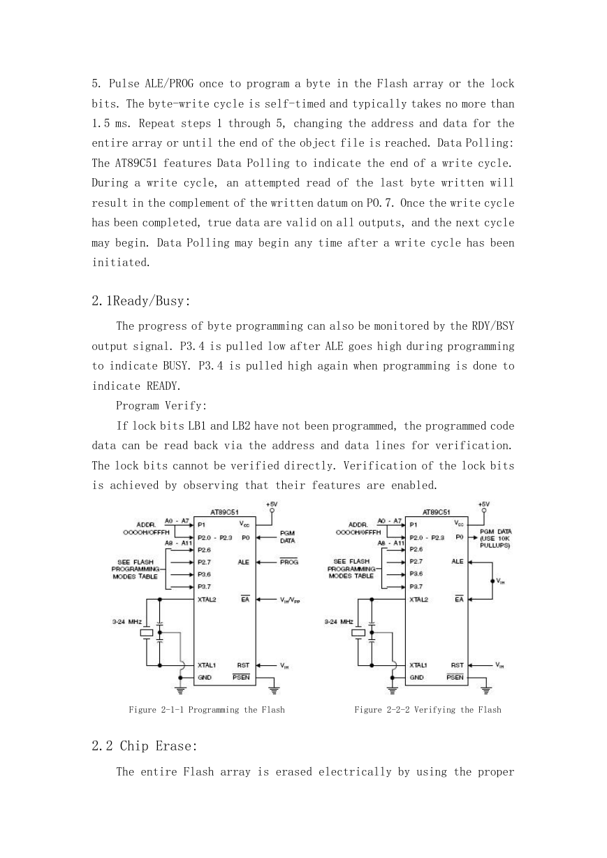
Before programming the AT89C51, the address, data and control signals
should be set up according to the Flash programming mode table and Figure
3 and Figure 4. To program the AT89C51, take the following steps.1. Input
the desired memory location on the address lines.2. Input the appropriate
data byte on the data lines. 3. Activate the correct combination of control
signals. 4. Raise EA/VPP to 12V for the high-voltage programming mode.
�
5. Pulse ALE/PROG once to program a byte in the Flash array or the lock
bits. The byte-write cycle is self-timed and typically takes no more than
1.5 ms. Repeat steps 1 through 5, changing the address and data for the
entire array or until the end of the object file is reached. Data Polling:
The AT89C51 features Data Polling to indicate the end of a write cycle.
During a write cycle, an attempted read of the last byte written will
result in the complement of the written datum on PO.7. Once the write cycle
has been completed, true data are valid on all outputs, and the next cycle
may begin. Data Polling may begin any time after a write cycle has been
initiated.
2.1Ready/Busy:
The progress of byte programming can also be monitored by the RDY/BSY
output signal. P3.4 is pulled low after ALE goes high during programming
to indicate BUSY. P3.4 is pulled high again when programming is done to
indicate READY.
Program Verify:
If lock bits LB1 and LB2 have not been programmed, the programmed code
data can be read back via the address and data lines for verification.
The lock bits cannot be verified directly. Verification of the lock bits
is achieved by observing that their features are enabled.
Figure 2-1-1 Programming the Flash
Figure 2-2-2 Verifying the Flash
2.2 Chip Erase:
The entire Flash array is erased electrically by using the proper
�
combination of control signals and by holding ALE/PROG low for 10 ms. The
code array is written with all “1”s. The chip erase operation must be
executed before the code memory can be re-programmed.
2.3 Reading the Signature Bytes:
The signature bytes are read by the same procedure as a normal
verification of locations 030H, 031H, and 032H, except that P3.6 and P3.7
must be pulled to a logic low. The values returned areas follows.
(030H) = 1EH indicates manufactured by Atmel
(031H) = 51H indicates 89C51
(032H) = FFH indicates 12V programming
(032H) = 05H indicates 5V programming
2.4 Programming Interface
Every code byte in the Flash array can be written and the entire array
can be erased by using the appropriate combination of control signals.
The write operation cycle is selftimed and once initiated, will
automatically time itself to completion. A microcomputer interface
converts information between two forms. Outside the microcomputer the
information handled by an electronic system exists as a physical signal,
but within the program, it is represented numerically. The function of
any interface can be broken down into a number of operations which modify
the data in some way, so that the process of conversion between the
external and internal forms is carried out in a number of steps. An
analog-to-digital converter(ADC) is used to convert a continuously
variable signal to a corresponding digital form which can take any one
of a fixed number of possible binary values. If the output of the
transducer does not vary continuously, no ADC is necessary. In this case
the signal conditioning section must convert the incoming signal to a form
which can be connected directly to the next part of the interface, the
input/output section of the microcomputer itself. Output interfaces take
a similar form, the obvious difference being that here the flow of
information is in the opposite direction; it is passed from the program
to the outside world. In this case the program may call an output
subroutine which supervises the operation of the interface and performs
�





 2023年江西萍乡中考道德与法治真题及答案.doc
 2012年重庆南川中考生物真题及答案.doc
 2013年江西师范大学地理学综合及文艺理论基础考研真题.doc
 2020年四川甘孜小升初语文真题及答案I卷.doc
 2020年注册岩土工程师专业基础考试真题及答案.doc
 2023-2024学年福建省厦门市九年级上学期数学月考试题及答案.doc
 2021-2022学年辽宁省沈阳市大东区九年级上学期语文期末试题及答案.doc
 2022-2023学年北京东城区初三第一学期物理期末试卷及答案.doc
 2018上半年江西教师资格初中地理学科知识与教学能力真题及答案.doc
 2012年河北国家公务员申论考试真题及答案-省级.doc
 2020-2021学年江苏省扬州市江都区邵樊片九年级上学期数学第一次质量检测试题及答案.doc
 2022下半年黑龙江教师资格证中学综合素质真题及答案.doc