1962
IEEE TRANSACTIONS ON MICROWAVE THEORY AND TECHNIQUES, VOL. 62, NO. 9, SEPTEMBER 2014
The Synthesis of Wide- and Multi-Bandgap
Electromagnetic Surfaces With Finite Size
and Nonuniform Capacitive Loading
Spencer H. Martin, Idellyse Martinez, Graduate Student Member, IEEE, Jeremiah P. Turpin, Member, IEEE,
Douglas H. Werner, Fellow, IEEE, Erik Lier, Fellow, IEEE, and Matthew G. Bray, Senior Member, IEEE
Abstract—A method is presented that allows for the efficient
design of capacitively loaded finite-size electromagnetic bandgap
(EBG) structures, which can target a wide range of design ob-
jectives. The design flexibility is achieved by adding arbitrary
nonuniform capacitive loading to an underlying periodic EBG
structure. This system can be interpreted as having an effective
aperiodic structure, which allows more design flexibility in terms
of bandgap engineering. To choose the proper capacitances, a
powerful global optimization technique known as the covariance
matrix adaptation evolutionary strategy is employed that is aided
by a fast port-reduction strategy. This approach avoids the need
to carry out multiple computationally expensive full-wave simula-
tions during the course of the optimization process by requiring
only a single full-wave simulation be performed prior to initiating
the optimization. To demonstrate the utility of this method, the
capacitive loading of a mushroom-type EBG structure in a par-
allel-plate waveguide is optimized to reduce transmission from 2.4
to 7 GHz. This design was fabricated and the measured response
was found to be in good agreement with the simulations. Using the
same initial full-wave simulation, another structure was designed
to improve isolation at the 2.4-, 3.6-, and 5-GHz WLAN bands to
below 22 dB. An additional set of structures are also designed
using capacitively loaded mushroom-type EBG surfaces without
placing them inside of a parallel-plate waveguide.
Index Terms—Aperiodic, capacitive loading, covariance matrix
adaptation evolutionary strategy (CMA-ES), electromagnetic
bandgap (EBG), multi-band, surface waves, wideband.
I. INTRODUCTION
T ECHNICAL developments in antenna engineering over
the past decade have been driven by the upsurge in the
variety and spatial density of wireless communications systems.
The need for efficient, low-profile, and high-gain antennas for
use in these communication applications represents a serious de-
sign challenge in the electromagnetics community. The recent
Manuscript received November 18, 2013; revised February 28, 2014 and May
11, 2014; accepted June 12, 2014. Date of publication July 16, 2014; date of
current version September 02, 2014. This work was supported in part under the
Lockheed Martin University Research Initiative (URI) Program.
S. H. Martin, I. Martinez, J. P. Turpin, and D. H. Werner are with the Depart-
ment of Electrical Engineering, The Pennsylvania State University, University
Park, PA 16802 USA (e-mail: svm5284@psu.edu; dhw@psu.edu).
E. Lier and M. G. Bray are with Lockheed Martin, Newtown, PA 18940 USA
Color versions of one or more of the figures in this paper are available online
(e-mail: erik.lier@lmco.com).
at http://ieeexplore.ieee.org.
Digital Object Identifier 10.1109/TMTT.2014.2335175
introduction of planar electromagnetic bandgap (EBG) struc-
tures has opened up the design space for the development of new
antenna systems that are capable of meeting these challenging
goals [1].
These structures, which act to stop the propagation of surface
waves, typically consist of electromagnetically soft surfaces
(e.g., corrugated surfaces) or subwavelength periodic metallic
sections printed on a thin dielectric substrate backed by a
ground plane. EBG surfaces offer a new design option when
improved surface-wave isolation between two or more antenna
elements is required. EBGs can also improve performance
when only a single antenna is present. In these cases, traditional
dielectric-coated ground planes can allow surface waves to
propagate to their edges and radiate, leading to a degraded gain
performance. In contrast, a properly designed periodic metallic
pattern printed on the dielectric substrate will act as an EBG to
reflect and contain the energy within the desired aperture with
in-phase reflected waves, thus improving the antenna gain and
radiation patterns.
The basic concept can be most easily understood from the
simple resonant circuit model of an inductor in parallel with a
capacitor. Individual device realizations vary depending on the
operational frequency and specific performance goals, but all
share similar properties. In Sievenpiper et al.’s mushroom-type
design, the capacitor represents the separation between adjacent
patches and the inductor represents the loop created between
unit cells by the vias [2]. A simplified side view of this type of
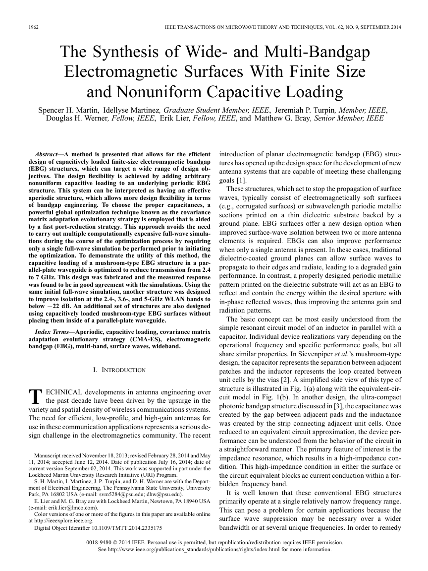
structure is illustrated in Fig. 1(a) along with the equivalent-cir-
cuit model in Fig. 1(b). In another design, the ultra-compact
photonic bandgap structure discussed in [3], the capacitance was
created by the gap between adjacent pads and the inductance
was created by the strip connecting adjacent unit cells. Once
reduced to an equivalent circuit approximation, the device per-
formance can be understood from the behavior of the circuit in
a straightforward manner. The primary feature of interest is the
impedance resonance, which results in a high-impedance con-
dition. This high-impedance condition in either the surface or
the circuit equivalent blocks ac current conduction within a for-
bidden frequency band.
It is well known that these conventional EBG structures
primarily operate at a single relatively narrow frequency range.
This can pose a problem for certain applications because the
surface wave suppression may be necessary over a wider
bandwidth or at several unique frequencies. In order to remedy
0018-9480 © 2014 IEEE. Personal use is permitted, but republication/redistribution requires IEEE permission.
See http://www.ieee.org/publications_standards/publications/rights/index.html for more information.
�
MARTIN et al.: SYNTHESIS OF WIDE- AND MULTI-BANDGAP ELECTROMAGNETIC SURFACES
1963
(a) Simplified representation of a mushroom-type structure along with
Fig. 1.
(b) its circuit equivalent model.
these problems, many previous studies have investigated cas-
cading together multiple sections with different properties. For
instance, in [4], the authors cascaded two mushroom-type unit
cells together. Each of these two distinct sections targeted a dif-
ferent frequency range. In order to achieve broader bandwidth,
the two frequency ranges overlap, which allows the overall
structure to provide isolation over the combined frequency
range. Using the same technique, multiple separated frequency
bands could also be targeted. However, a significant limitation
to this approach is the rapid increase in physical size, which
results each time the frequency range is expanded. This can
often be problematic, especially when there exists a predefined
spacing limitation between the antenna elements that are being
targeted for isolation.
Another method that has been used to achieve a similar effect
is to add lumped elements to the structure rather than varying
the unit-cell dimensions [5]. This method offers several advan-
tages. First, the underlying structure is completely periodic and
lumped capacitors are used to modify the natural capacitance of
the surface and thereby alter the resonant frequency. The second
advantage is that, analogous to the circuit model, the resonant
frequency will be reduced by the addition of capacitors. This
allows for the structure to be effectively more compact when
compared to wavelength.
Although inductors might also be used to achieve this effect,
several considerations discourage this. The main reason is the
complexity to manufacture such structures, due to the placement
of the lumped inductor. To modify the natural inductance of the
structure, the loaded element must be in series. For example,
in [6], the added inductance was connected in the via-ground
plane. Incorporating inductors in this manner causes the fre-
quency to shift to a lower range, as discussed in [7], which can
be exploited to add more degrees of freedom; however, the com-
plexity for building such a structure will also be increased. An
alternative would be to use magnetic materials to increase the
inductance [8], but this is often considered impractical due to
the loss in many magnetic materials, as well as the increased
weight and cost. Furthermore, additional capacitance usually in-
troduces enough flexibility to achieve the desired goals; there-
fore the additional degrees of freedom that could be introduced
by considering inductance are typically not necessary.
Similar to the capacitively loaded multi-section EBG concept
mentioned above, our proposed method also modifies the struc-
ture by incorporating additional capacitance into the unit cells.
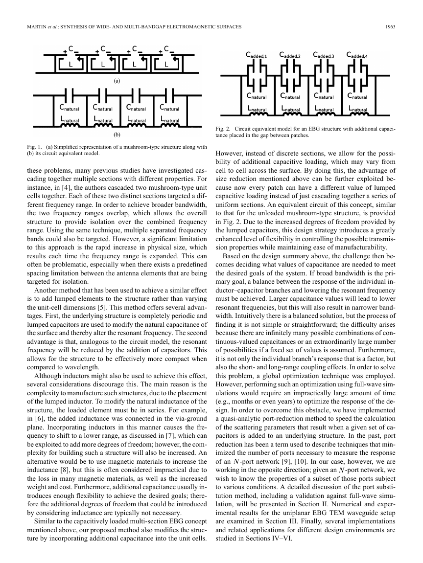
Fig. 2. Circuit equivalent model for an EBG structure with additional capaci-
tance placed in the gap between patches.
However, instead of discrete sections, we allow for the possi-
bility of additional capacitive loading, which may vary from
cell to cell across the surface. By doing this, the advantage of
size reduction mentioned above can be further exploited be-
cause now every patch can have a different value of lumped
capacitive loading instead of just cascading together a series of
uniform sections. An equivalent circuit of this concept, similar
to that for the unloaded mushroom-type structure, is provided
in Fig. 2. Due to the increased degrees of freedom provided by
the lumped capacitors, this design strategy introduces a greatly
enhanced level of flexibility in controlling the possible transmis-
sion properties while maintaining ease of manufacturability.
Based on the design summary above, the challenge then be-
comes deciding what values of capacitance are needed to meet
the desired goals of the system. If broad bandwidth is the pri-
mary goal, a balance between the response of the individual in-
ductor–capacitor branches and lowering the resonant frequency
must be achieved. Larger capacitance values will lead to lower
resonant frequencies, but this will also result in narrower band-
width. Intuitively there is a balanced solution, but the process of
finding it is not simple or straightforward; the difficulty arises
because there are infinitely many possible combinations of con-
tinuous-valued capacitances or an extraordinarily large number
of possibilities if a fixed set of values is assumed. Furthermore,
it is not only the individual branch’s response that is a factor, but
also the short- and long-range coupling effects. In order to solve
this problem, a global optimization technique was employed.
However, performing such an optimization using full-wave sim-
ulations would require an impractically large amount of time
(e.g., months or even years) to optimize the response of the de-
sign. In order to overcome this obstacle, we have implemented
a quasi-analytic port-reduction method to speed the calculation
of the scattering parameters that result when a given set of ca-
pacitors is added to an underlying structure. In the past, port
reduction has been a term used to describe techniques that min-
imized the number of ports necessary to measure the response
of an
-port network [9], [10]. In our case, however, we are
working in the opposite direction; given an
-port network, we
wish to know the properties of a subset of those ports subject
to various conditions. A detailed discussion of the port substi-
tution method, including a validation against full-wave simu-
lation, will be presented in Section II. Numerical and exper-
imental results for the uniplanar EBG TEM waveguide setup
are examined in Section III. Finally, several implementations
and related applications for different design environments are
studied in Sections IV–VI.
�
1964
IEEE TRANSACTIONS ON MICROWAVE THEORY AND TECHNIQUES, VOL. 62, NO. 9, SEPTEMBER 2014
been substituted. This procedure takes fractions of a second
as opposed to the lengthy process of a full-wave simulation.
Due to this fact, this method may be readily integrated into an
optimization procedure, which can utilized to determine the
appropriate values of the loaded lumped elements based on a
desired behavior of the EBG [12], [13].
B. Verification
In order to demonstrate the utility of the procedure outlined
in Section II-A, port substitution will be compared to a tradi-
tional full-wave simulation with lumped elements. To accom-
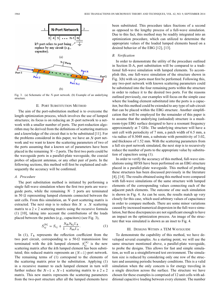
plish this, one full-wave simulation of the structure shown in
Fig. 3(b) with six ports must first be performed. Following this,
any two-port network with known scattering parameters could
be substituted into the four remaining ports within the structure
in order to reduce it to the desired two ports. For the reasons
outlined previously, our examples will focus on the simple case
where the loading element substituted into the ports is a capac-
itor, but this method could be extended to any type of sub-circuit
that can be placed within the EBG structure. Another simplifi-
cation that will be employed for the remainder of this paper is
to assume that the underlying (unloaded) structure is a mush-
room-type EBG surface designed to have a resonant frequency
approximately at 7 GHz. The underlying structure will have a
unit cell with periodicity of 7 mm, a patch width of 6.5 mm, a
via radius of 0.3048 mm, a substrate with permittivity of 3.02,
and thickness of 1.52 mm. With the scattering parameters from
a full six-port network simulated, the next step is to recursively
reduce the number of ports to the appropriate value by substitu-
tion of capacitors using (1).
In order to verify the accuracy of this method, full-wave sim-
ulations using HFSS have been performed on an EBG structure
placed in a parallel-plate waveguide. This method of probing
these structures has been discussed previously in the literature
[4], [14]. The results obtained using this method were compared
with full-wave simulations of the same structure with lumped
elements of the corresponding values connecting each of the
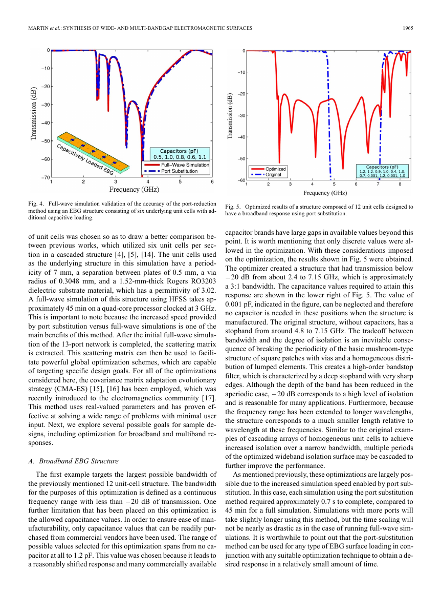
adjacent patch elements. The outcome of one such simulation
is shown in Fig. 4. As can be seen, the results match up very
closely for this case, which used arbitrary values of capacitance
in order to compare methods. There are some minor variations
caused by increased numerical dispersion in the full-wave simu-
lation, but these discrepancies are not significant enough to have
an impact on the optimization process. An image of the struc-
ture that was simulated is shown as an inset to Fig. 4.
III. DESIGNS WITHIN A TEM WAVEGUIDE
To demonstrate the capability of this method, we have de-
veloped several examples. As a starting point, we will use the
same structure mentioned above, a parallel-plate waveguide,
to probe the designs. This allows for fast and simple simula-
tion, as well as a straightforward test environment. The simula-
tion size is reduced by considering only one row of the struc-
ture and assuming periodic boundary conditions. This is a valid
simulation when the only concern is for energy traveling in
a single direction across the surface. The structure we have
chosen for these examples is comprised of 12 unit cells with ad-
ditional capacitive loading between every element. The number
Fig. 3.
structure.
(a) Schematic of the
-port network. (b) Example of an underlying
II. PORT SUBSTITUTION METHOD
The aim of the port-substitution method is to overcome the
length optimization process, which involves the use of lumped
structures; its focus is on reducing an
-port network to a net-
work with a smaller number of ports. The port-reduction algo-
rithm may be derived from the definitions of scattering matrices
and a knowledge of the circuit that is to be substituted [11]. For
the problems considered in this paper, we have an
-port net-
work and we want to know the scattering parameters of two of
the ports assuming that a known set of parameters have been
placed in the remaining
ports. The first two ports could be
the waveguide ports in a parallel-plate waveguide, the coaxial
probes of adjacent antennas, or any other pair of ports. In the
following sections, this method will first be explained and sub-
sequently the accuracy will be confirmed.
A. Procedure
The port substitution method is initiated by performing a
single full-wave simulation where the first two ports are wave-
guide ports, while the remaining
ports are terminated
in 50
representing lumped elements connected between the
unit cells. From this simulation, an
-port scattering matrix is
extracted. The next step is to reduce this
scattering
matrix to a 2
2 scattering matrix using the recursive formula
(1) [10], taking into account the contributions of the loads
placed between the patches (e.g., capacitors) (see Fig. 3),
(1)
In (1),
th lumped element.
represents the reflection coefficient from the
two port circuit, corresponding to a 50-
transmission line
is the new
terminated with the
scattering matrix after the th lumped element has been substi-
tuted; this reduced matrix represents an
-port network.
The remaining terms of (1) correspond to the elements of
the scattering matrix prior to the substitution. Applying (1)
in a recursive manner to each lumped element in turn will
further reduce the
2
matrix. This new matrix represents the scattering parameters
from the two-port structure after all the lumped elements have
scattering matrix to a 2
�
MARTIN et al.: SYNTHESIS OF WIDE- AND MULTI-BANDGAP ELECTROMAGNETIC SURFACES
1965
Fig. 4. Full-wave simulation validation of the accuracy of the port-reduction
method using an EBG structure consisting of six underlying unit cells with ad-
ditional capacitive loading.
Fig. 5. Optimized results of a structure composed of 12 unit cells designed to
have a broadband response using port substitution.
of unit cells was chosen so as to draw a better comparison be-
tween previous works, which utilized six unit cells per sec-
tion in a cascaded structure [4], [5], [14]. The unit cells used
as the underlying structure in this simulation have a period-
icity of 7 mm, a separation between plates of 0.5 mm, a via
radius of 0.3048 mm, and a 1.52-mm-thick Rogers RO3203
dielectric substrate material, which has a permittivity of 3.02.
A full-wave simulation of this structure using HFSS takes ap-
proximately 45 min on a quad-core processor clocked at 3 GHz.
This is important to note because the increased speed provided
by port substitution versus full-wave simulations is one of the
main benefits of this method. After the initial full-wave simula-
tion of the 13-port network is completed, the scattering matrix
is extracted. This scattering matrix can then be used to facili-
tate powerful global optimization schemes, which are capable
of targeting specific design goals. For all of the optimizations
considered here, the covariance matrix adaptation evolutionary
strategy (CMA-ES) [15], [16] has been employed, which was
recently introduced to the electromagnetics community [17].
This method uses real-valued parameters and has proven ef-
fective at solving a wide range of problems with minimal user
input. Next, we explore several possible goals for sample de-
signs, including optimization for broadband and multiband re-
sponses.
A. Broadband EBG Structure
The first example targets the largest possible bandwidth of
the previously mentioned 12 unit-cell structure. The bandwidth
for the purposes of this optimization is defined as a continuous
frequency range with less than
20 dB of transmission. One
further limitation that has been placed on this optimization is
the allowed capacitance values. In order to ensure ease of man-
ufacturability, only capacitance values that can be readily pur-
chased from commercial vendors have been used. The range of
possible values selected for this optimization spans from no ca-
pacitor at all to 1.2 pF. This value was chosen because it leads to
a reasonably shifted response and many commercially available
capacitor brands have large gaps in available values beyond this
point. It is worth mentioning that only discrete values were al-
lowed in the optimization. With these considerations imposed
on the optimization, the results shown in Fig. 5 were obtained.
The optimizer created a structure that had transmission below
20 dB from about 2.4 to 7.15 GHz, which is approximately
a 3:1 bandwidth. The capacitance values required to attain this
response are shown in the lower right of Fig. 5. The value of
0.001 pF, indicated in the figure, can be neglected and therefore
no capacitor is needed in these positions when the structure is
manufactured. The original structure, without capacitors, has a
stopband from around 4.8 to 7.15 GHz. The tradeoff between
bandwidth and the degree of isolation is an inevitable conse-
quence of breaking the periodicity of the basic mushroom-type
structure of square patches with vias and a homogeneous distri-
bution of lumped elements. This creates a high-order bandstop
filter, which is characterized by a deep stopband with very sharp
edges. Although the depth of the band has been reduced in the
aperiodic case,
20 dB corresponds to a high level of isolation
and is reasonable for many applications. Furthermore, because
the frequency range has been extended to longer wavelengths,
the structure corresponds to a much smaller length relative to
wavelength at these frequencies. Similar to the original exam-
ples of cascading arrays of homogeneous unit cells to achieve
increased isolation over a narrow bandwidth, multiple periods
of the optimized wideband isolation surface may be cascaded to
further improve the performance.
As mentioned previously, these optimizations are largely pos-
sible due to the increased simulation speed enabled by port sub-
stitution. In this case, each simulation using the port substitution
method required approximately 0.7 s to complete, compared to
45 min for a full simulation. Simulations with more ports will
take slightly longer using this method, but the time scaling will
not be nearly as drastic as in the case of running full-wave sim-
ulations. It is worthwhile to point out that the port-substitution
method can be used for any type of EBG surface loading in con-
junction with any suitable optimization technique to obtain a de-
sired response in a relatively small amount of time.
�
1966
IEEE TRANSACTIONS ON MICROWAVE THEORY AND TECHNIQUES, VOL. 62, NO. 9, SEPTEMBER 2014
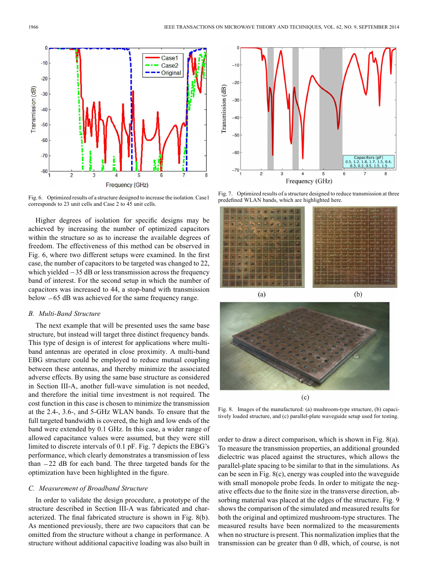
Fig. 6. Optimized results of a structure designed to increase the isolation. Case1
corresponds to 23 unit cells and Case 2 to 45 unit cells.
Higher degrees of isolation for specific designs may be
achieved by increasing the number of optimized capacitors
within the structure so as to increase the available degrees of
freedom. The effectiveness of this method can be observed in
Fig. 6, where two different setups were examined. In the first
case, the number of capacitors to be targeted was changed to 22,
which yielded 35 dB or less transmission across the frequency
band of interest. For the second setup in which the number of
capacitors was increased to 44, a stop-band with transmission
below 65 dB was achieved for the same frequency range.
B. Multi-Band Structure
The next example that will be presented uses the same base
structure, but instead will target three distinct frequency bands.
This type of design is of interest for applications where multi-
band antennas are operated in close proximity. A multi-band
EBG structure could be employed to reduce mutual coupling
between these antennas, and thereby minimize the associated
adverse effects. By using the same base structure as considered
in Section III-A, another full-wave simulation is not needed,
and therefore the initial time investment is not required. The
cost function in this case is chosen to minimize the transmission
at the 2.4-, 3.6-, and 5-GHz WLAN bands. To ensure that the
full targeted bandwidth is covered, the high and low ends of the
band were extended by 0.1 GHz. In this case, a wider range of
allowed capacitance values were assumed, but they were still
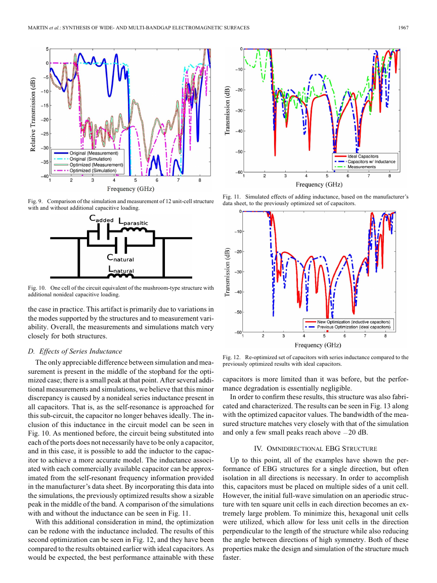
limited to discrete intervals of 0.1 pF. Fig. 7 depicts the EBG’s
performance, which clearly demonstrates a transmission of less
than
22 dB for each band. The three targeted bands for the
optimization have been highlighted in the figure.
C. Measurement of Broadband Structure
In order to validate the design procedure, a prototype of the
structure described in Section III-A was fabricated and char-
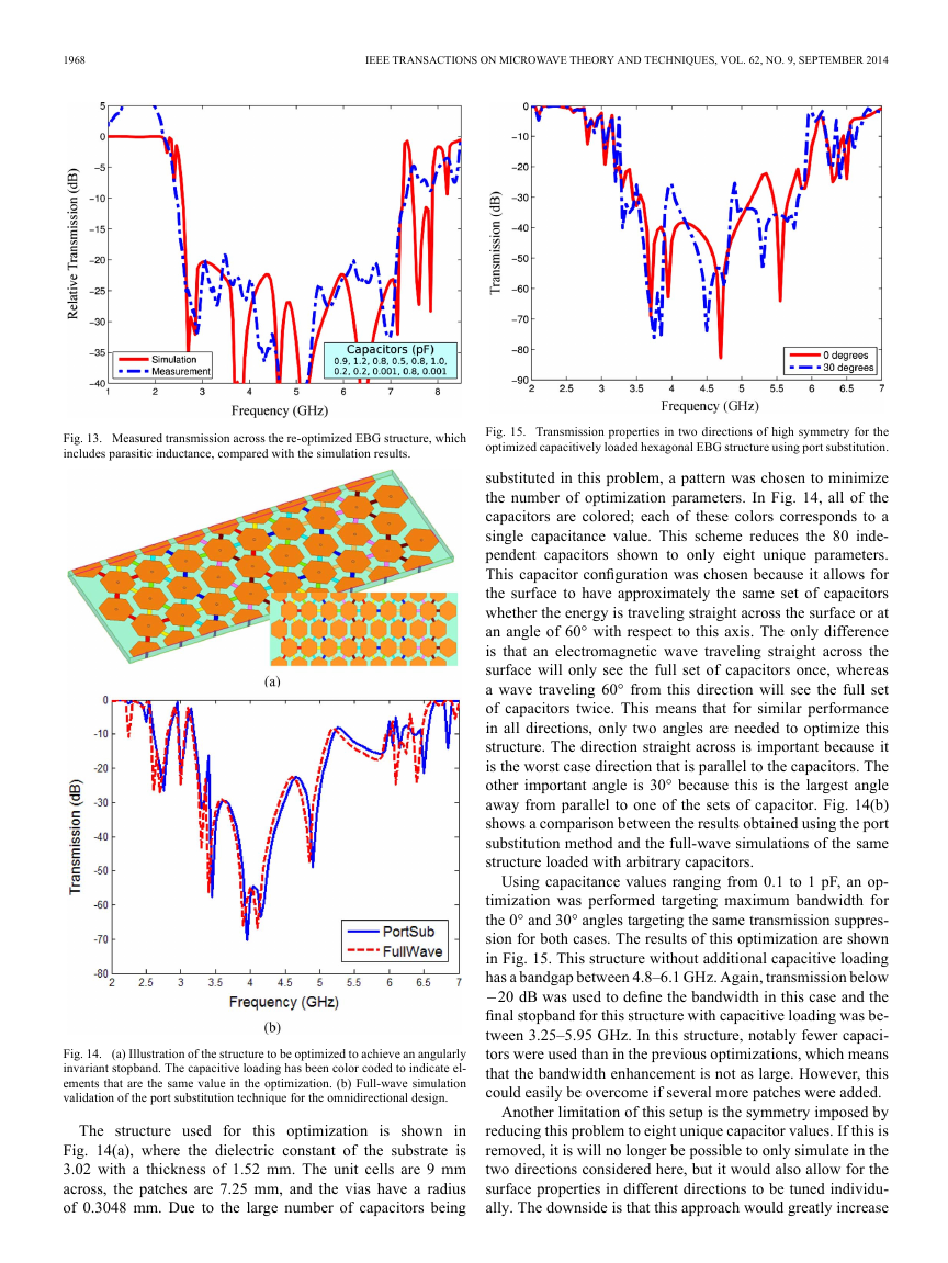
acterized. The final fabricated structure is shown in Fig. 8(b).
As mentioned previously, there are two capacitors that can be
omitted from the structure without a change in performance. A
structure without additional capacitive loading was also built in
Fig. 7. Optimized results of a structure designed to reduce transmission at three
predefined WLAN bands, which are highlighted here.
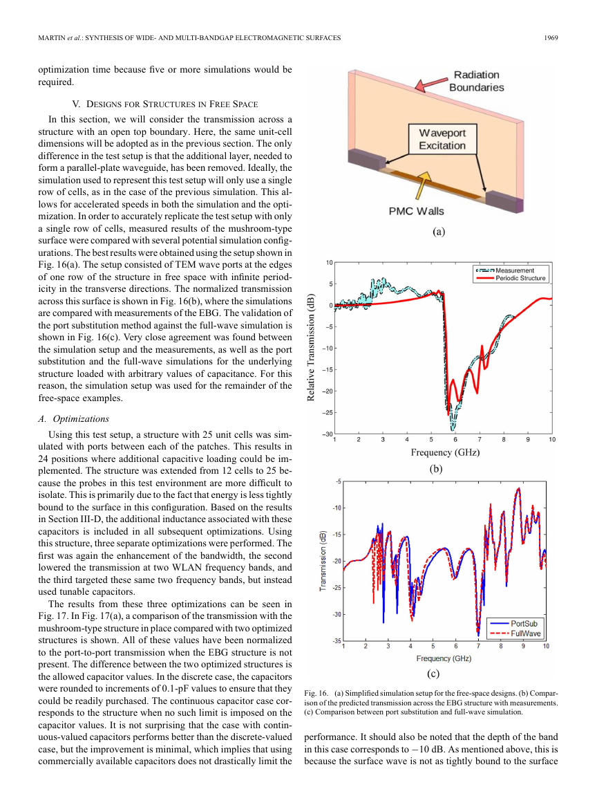
Fig. 8.
Images of the manufactured: (a) mushroom-type structure, (b) capaci-
tively loaded structure, and (c) parallel-plate waveguide setup used for testing.
order to draw a direct comparison, which is shown in Fig. 8(a).
To measure the transmission properties, an additional grounded
dielectric was placed against the structures, which allows the
parallel-plate spacing to be similar to that in the simulations. As
can be seen in Fig. 8(c), energy was coupled into the waveguide
with small monopole probe feeds. In order to mitigate the neg-
ative effects due to the finite size in the transverse direction, ab-
sorbing material was placed at the edges of the structure. Fig. 9
shows the comparison of the simulated and measured results for
both the original and optimized mushroom-type structures. The
measured results have been normalized to the measurements
when no structure is present. This normalization implies that the
transmission can be greater than 0 dB, which, of course, is not
�
MARTIN et al.: SYNTHESIS OF WIDE- AND MULTI-BANDGAP ELECTROMAGNETIC SURFACES
1967
Fig. 9. Comparison of the simulation and measurement of 12 unit-cell structure
with and without additional capacitive loading.
Fig. 11. Simulated effects of adding inductance, based on the manufacturer’s
data sheet, to the previously optimized set of capacitors.
Fig. 10. One cell of the circuit equivalent of the mushroom-type structure with
additional nonideal capacitive loading.
the case in practice. This artifact is primarily due to variations in
the modes supported by the structures and to measurement vari-
ability. Overall, the measurements and simulations match very
closely for both structures.
D. Effects of Series Inductance
The only appreciable difference between simulation and mea-
surement is present in the middle of the stopband for the opti-
mized case; there is a small peak at that point. After several addi-
tional measurements and simulations, we believe that this minor
discrepancy is caused by a nonideal series inductance present in
all capacitors. That is, as the self-resonance is approached for
this sub-circuit, the capacitor no longer behaves ideally. The in-
clusion of this inductance in the circuit model can be seen in
Fig. 10. As mentioned before, the circuit being substituted into
each of the ports does not necessarily have to be only a capacitor,
and in this case, it is possible to add the inductor to the capac-
itor to achieve a more accurate model. The inductance associ-
ated with each commercially available capacitor can be approx-
imated from the self-resonant frequency information provided
in the manufacturer’s data sheet. By incorporating this data into
the simulations, the previously optimized results show a sizable
peak in the middle of the band. A comparison of the simulations
with and without the inductance can be seen in Fig. 11.
With this additional consideration in mind, the optimization
can be redone with the inductance included. The results of this
second optimization can be seen in Fig. 12, and they have been
compared to the results obtained earlier with ideal capacitors. As
would be expected, the best performance attainable with these
Fig. 12. Re-optimized set of capacitors with series inductance compared to the
previously optimized results with ideal capacitors.
capacitors is more limited than it was before, but the perfor-
mance degradation is essentially negligible.
In order to confirm these results, this structure was also fabri-
cated and characterized. The results can be seen in Fig. 13 along
with the optimized capacitor values. The bandwidth of the mea-
sured structure matches very closely with that of the simulation
and only a few small peaks reach above
20 dB.
IV. OMNIDIRECTIONAL EBG STRUCTURE
Up to this point, all of the examples have shown the per-
formance of EBG structures for a single direction, but often
isolation in all directions is necessary. In order to accomplish
this, capacitors must be placed on multiple sides of a unit cell.
However, the initial full-wave simulation on an aperiodic struc-
ture with ten square unit cells in each direction becomes an ex-
tremely large problem. To minimize this, hexagonal unit cells
were utilized, which allow for less unit cells in the direction
perpendicular to the length of the structure while also reducing
the angle between directions of high symmetry. Both of these
properties make the design and simulation of the structure much
faster.
�
1968
IEEE TRANSACTIONS ON MICROWAVE THEORY AND TECHNIQUES, VOL. 62, NO. 9, SEPTEMBER 2014
Fig. 13. Measured transmission across the re-optimized EBG structure, which
includes parasitic inductance, compared with the simulation results.
Fig. 14.
(a) Illustration of the structure to be optimized to achieve an angularly
invariant stopband. The capacitive loading has been color coded to indicate el-
ements that are the same value in the optimization. (b) Full-wave simulation
validation of the port substitution technique for the omnidirectional design.
The structure used for
this optimization is shown in
Fig. 14(a), where the dielectric constant of the substrate is
3.02 with a thickness of 1.52 mm. The unit cells are 9 mm
across, the patches are 7.25 mm, and the vias have a radius
of 0.3048 mm. Due to the large number of capacitors being
Fig. 15. Transmission properties in two directions of high symmetry for the
optimized capacitively loaded hexagonal EBG structure using port substitution.
substituted in this problem, a pattern was chosen to minimize
the number of optimization parameters. In Fig. 14, all of the
capacitors are colored; each of these colors corresponds to a
single capacitance value. This scheme reduces the 80 inde-
pendent capacitors shown to only eight unique parameters.
This capacitor configuration was chosen because it allows for
the surface to have approximately the same set of capacitors
whether the energy is traveling straight across the surface or at
an angle of 60° with respect to this axis. The only difference
is that an electromagnetic wave traveling straight across the
surface will only see the full set of capacitors once, whereas
a wave traveling 60° from this direction will see the full set
of capacitors twice. This means that for similar performance
in all directions, only two angles are needed to optimize this
structure. The direction straight across is important because it
is the worst case direction that is parallel to the capacitors. The
other important angle is 30° because this is the largest angle
away from parallel to one of the sets of capacitor. Fig. 14(b)
shows a comparison between the results obtained using the port
substitution method and the full-wave simulations of the same
structure loaded with arbitrary capacitors.
Using capacitance values ranging from 0.1 to 1 pF, an op-
timization was performed targeting maximum bandwidth for
the 0° and 30° angles targeting the same transmission suppres-
sion for both cases. The results of this optimization are shown
in Fig. 15. This structure without additional capacitive loading
has a bandgap between 4.8–6.1 GHz. Again, transmission below
20 dB was used to define the bandwidth in this case and the
final stopband for this structure with capacitive loading was be-
tween 3.25–5.95 GHz. In this structure, notably fewer capaci-
tors were used than in the previous optimizations, which means
that the bandwidth enhancement is not as large. However, this
could easily be overcome if several more patches were added.
Another limitation of this setup is the symmetry imposed by
reducing this problem to eight unique capacitor values. If this is
removed, it is will no longer be possible to only simulate in the
two directions considered here, but it would also allow for the
surface properties in different directions to be tuned individu-
ally. The downside is that this approach would greatly increase
�
MARTIN et al.: SYNTHESIS OF WIDE- AND MULTI-BANDGAP ELECTROMAGNETIC SURFACES
1969
optimization time because five or more simulations would be
required.
V. DESIGNS FOR STRUCTURES IN FREE SPACE
In this section, we will consider the transmission across a
structure with an open top boundary. Here, the same unit-cell
dimensions will be adopted as in the previous section. The only
difference in the test setup is that the additional layer, needed to
form a parallel-plate waveguide, has been removed. Ideally, the
simulation used to represent this test setup will only use a single
row of cells, as in the case of the previous simulation. This al-
lows for accelerated speeds in both the simulation and the opti-
mization. In order to accurately replicate the test setup with only
a single row of cells, measured results of the mushroom-type
surface were compared with several potential simulation config-
urations. The best results were obtained using the setup shown in
Fig. 16(a). The setup consisted of TEM wave ports at the edges
of one row of the structure in free space with infinite period-
icity in the transverse directions. The normalized transmission
across this surface is shown in Fig. 16(b), where the simulations
are compared with measurements of the EBG. The validation of
the port substitution method against the full-wave simulation is
shown in Fig. 16(c). Very close agreement was found between
the simulation setup and the measurements, as well as the port
substitution and the full-wave simulations for the underlying
structure loaded with arbitrary values of capacitance. For this
reason, the simulation setup was used for the remainder of the
free-space examples.
A. Optimizations
Using this test setup, a structure with 25 unit cells was sim-
ulated with ports between each of the patches. This results in
24 positions where additional capacitive loading could be im-
plemented. The structure was extended from 12 cells to 25 be-
cause the probes in this test environment are more difficult to
isolate. This is primarily due to the fact that energy is less tightly
bound to the surface in this configuration. Based on the results
in Section III-D, the additional inductance associated with these
capacitors is included in all subsequent optimizations. Using
this structure, three separate optimizations were performed. The
first was again the enhancement of the bandwidth, the second
lowered the transmission at two WLAN frequency bands, and
the third targeted these same two frequency bands, but instead
used tunable capacitors.
The results from these three optimizations can be seen in
Fig. 17. In Fig. 17(a), a comparison of the transmission with the
mushroom-type structure in place compared with two optimized
structures is shown. All of these values have been normalized
to the port-to-port transmission when the EBG structure is not
present. The difference between the two optimized structures is
the allowed capacitor values. In the discrete case, the capacitors
were rounded to increments of 0.1-pF values to ensure that they
could be readily purchased. The continuous capacitor case cor-
responds to the structure when no such limit is imposed on the
capacitor values. It is not surprising that the case with contin-
uous-valued capacitors performs better than the discrete-valued
case, but the improvement is minimal, which implies that using
commercially available capacitors does not drastically limit the
Fig. 16.
(a) Simplified simulation setup for the free-space designs. (b) Compar-
ison of the predicted transmission across the EBG structure with measurements.
(c) Comparison between port substitution and full-wave simulation.
performance. It should also be noted that the depth of the band
in this case corresponds to
10 dB. As mentioned above, this is
because the surface wave is not as tightly bound to the surface
�


 2023年江西萍乡中考道德与法治真题及答案.doc
 2012年重庆南川中考生物真题及答案.doc
 2013年江西师范大学地理学综合及文艺理论基础考研真题.doc
 2020年四川甘孜小升初语文真题及答案I卷.doc
 2020年注册岩土工程师专业基础考试真题及答案.doc
 2023-2024学年福建省厦门市九年级上学期数学月考试题及答案.doc
 2021-2022学年辽宁省沈阳市大东区九年级上学期语文期末试题及答案.doc
 2022-2023学年北京东城区初三第一学期物理期末试卷及答案.doc
 2018上半年江西教师资格初中地理学科知识与教学能力真题及答案.doc
 2012年河北国家公务员申论考试真题及答案-省级.doc
 2020-2021学年江苏省扬州市江都区邵樊片九年级上学期数学第一次质量检测试题及答案.doc
 2022下半年黑龙江教师资格证中学综合素质真题及答案.doc