Preface
Key Design-for-Test Flows and Methodologies
Design-for-Test Flows in the Logical Domain
Unmapped Design Flow
Synthesizing Your Design
Postprocessing Your Design
Building Scan Chains
Mapped Design Flow
Reading In Your Design
Performing Scan Replacement and Building Scan Chains
Mapped Designs With Existing Scan Flow
Reading In Your Design
Checking Test Design Rules
Designing Block by Block
Controlling Scan Replacement During Scan Insertion
Hierarchical Scan Synthesis Flow
Introduction to Test Models
Linking Test Models to Library Cells
Checking If a Library Contains CTL Models
Scan Assembly Using Test Models
Saving Test Models for Subdesigns
Using Test Models
Reading Designs Into TetraMAX
Managing Test Models
Top-Level Integration
Hierarchical ScanEnable Integration
DFT Flows in Design Compiler Topographical Mode
Supported DFT Features
DFT Insertion Flow in Design Compiler Topographical Mode
Running DFT Insertion in Design Compiler Topographical Mode
Error Messages
Hierarchical Support in Design Compiler Topographical Mode
Top-Level Design Stitching Flow
Bottom-Up/Hierarchical Flow With Test Models
Scan Insertion Methodologies
Bottom-Up Scan Insertion
Top-Down Scan Insertion
DFT Compiler Default Scan Synthesis Approach
Scan Replacement
Scan Element Allocation
Test Signals
Pad Cells
Area and Timing Optimization
Getting the Best Results With Scan Design
DFT Compiler and Power Compiler Interoperability
Improving Testability in Clock Gating
Inserting Control Points in Control Clock Gating
Scan Enable Versus Test Mode
Inserting Observation Points to Control Clock Gating
Choosing a Depth for Observability Logic
Power Compiler/DFT Compiler Interoperability Flows
Using test_mode With Power Compiler
Using Scan Enables With Power Compiler
Connecting Test Pins to Clock-Gating Cells Using insert_dft
Design Requirements
Hookup Testport Connections
Design Rule Checking Changes
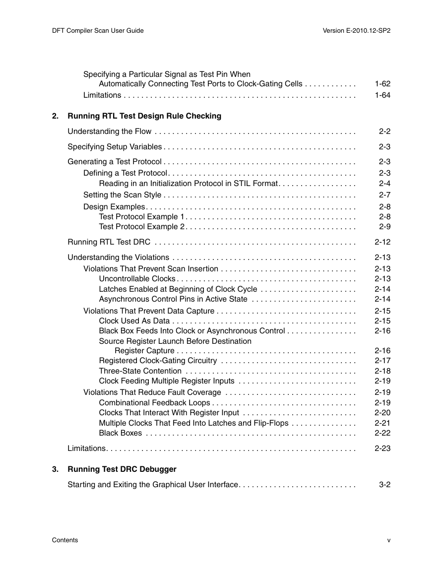
Specifying a Particular Signal as Test Pin When Automatically Connecting Test Ports to Clock-Gating Cells
Limitations
Running RTL Test Design Rule Checking
Understanding the Flow
Specifying Setup Variables
Generating a Test Protocol
Defining a Test Protocol
Reading in an Initialization Protocol in STIL Format
Setting the Scan Style
Design Examples
Test Protocol Example 1
Test Protocol Example 2
Running RTL Test DRC
Understanding the Violations
Violations That Prevent Scan Insertion
Uncontrollable Clocks
Latches Enabled at Beginning of Clock Cycle
Asynchronous Control Pins in Active State
Violations That Prevent Data Capture
Clock Used As Data
Black Box Feeds Into Clock or Asynchronous Control
Source Register Launch Before Destination Register Capture
Registered Clock-Gating Circuitry
Three-State Contention
Clock Feeding Multiple Register Inputs
Violations That Reduce Fault Coverage
Combinational Feedback Loops
Clocks That Interact With Register Input
Multiple Clocks That Feed Into Latches and Flip-Flops
Black Boxes
Limitations
Running Test DRC Debugger
Starting and Exiting the Graphical User Interface
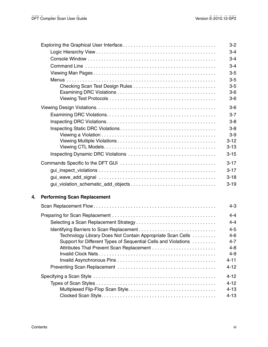
Exploring the Graphical User Interface
Logic Hierarchy View
Console Window
Command Line
Viewing Man Pages
Menus
Checking Scan Test Design Rules
Examining DRC Violations
Viewing Test Protocols
Viewing Design Violations
Examining DRC Violations
Inspecting DRC Violations
Inspecting Static DRC Violations
Viewing a Violation
Viewing Multiple Violations
Viewing CTL Models
Inspecting Dynamic DRC Violations
Commands Specific to the DFT GUI
gui_inspect_violations
gui_wave_add_signal
gui_violation_schematic_add_objects
Performing Scan Replacement
Scan Replacement Flow
Preparing for Scan Replacement
Selecting a Scan Replacement Strategy
Identifying Barriers to Scan Replacement
Technology Library Does Not Contain Appropriate Scan Cells
Support for Different Types of Sequential Cells and Violations
Attributes That Prevent Scan Replacement
Invalid Clock Nets
Invalid Asynchronous Pins
Preventing Scan Replacement
Specifying a Scan Style
Types of Scan Styles
Multiplexed Flip-Flop Scan Style
Clocked Scan Style
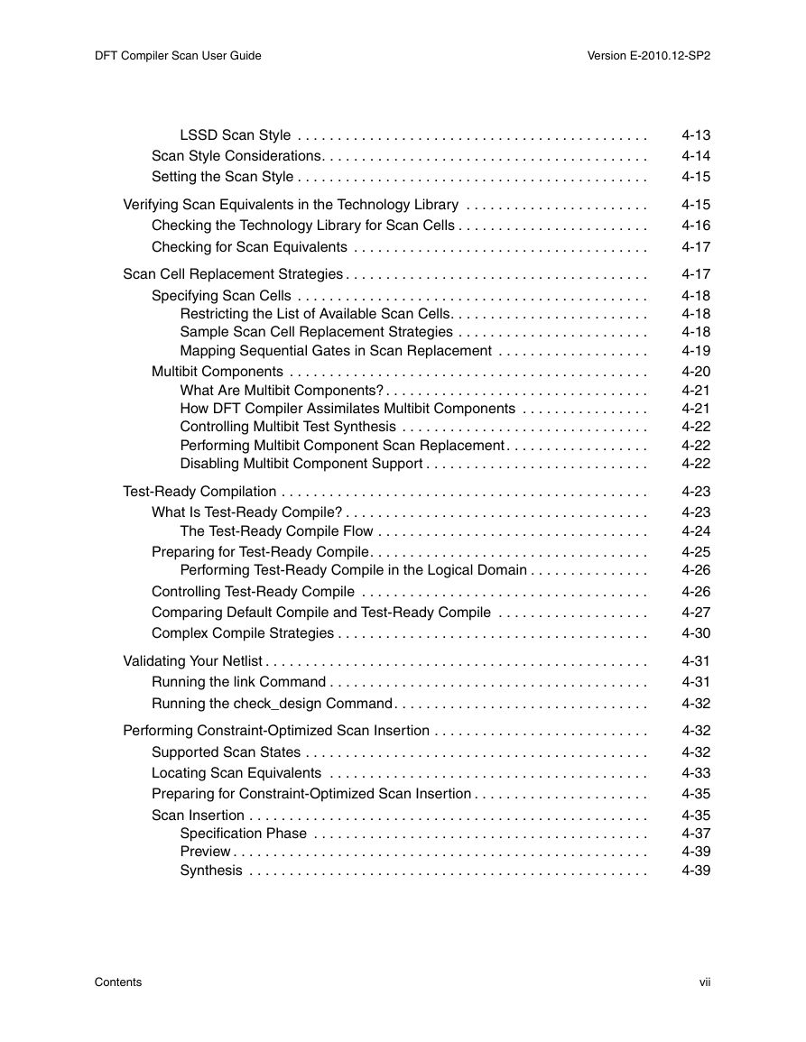
LSSD Scan Style
Scan Style Considerations
Setting the Scan Style
Verifying Scan Equivalents in the Technology Library
Checking the Technology Library for Scan Cells
Checking for Scan Equivalents
Scan Cell Replacement Strategies
Specifying Scan Cells
Restricting the List of Available Scan Cells
Sample Scan Cell Replacement Strategies
Mapping Sequential Gates in Scan Replacement
Multibit Components
What Are Multibit Components?
How DFT Compiler Assimilates Multibit Components
Controlling Multibit Test Synthesis
Performing Multibit Component Scan Replacement
Disabling Multibit Component Support
Test-Ready Compilation
What Is Test-Ready Compile?
The Test-Ready Compile Flow
Preparing for Test-Ready Compile
Performing Test-Ready Compile in the Logical Domain
Controlling Test-Ready Compile
Comparing Default Compile and Test-Ready Compile
Complex Compile Strategies
Validating Your Netlist
Running the link Command
Running the check_design Command
Performing Constraint-Optimized Scan Insertion
Supported Scan States
Locating Scan Equivalents
Preparing for Constraint-Optimized Scan Insertion
Scan Insertion
Specification Phase
Preview
Synthesis
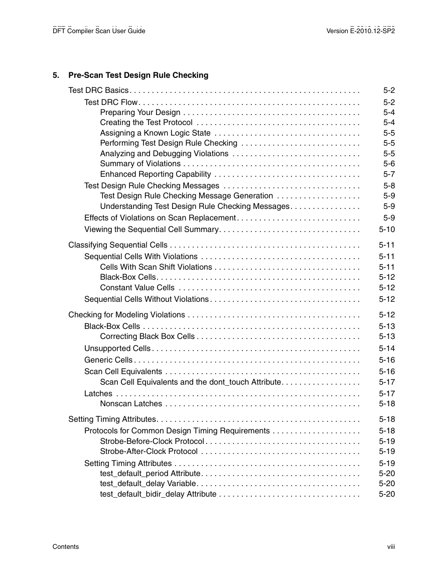
Pre-Scan Test Design Rule Checking
Test DRC Basics
Test DRC Flow
Preparing Your Design
Creating the Test Protocol
Assigning a Known Logic State
Performing Test Design Rule Checking
Analyzing and Debugging Violations
Summary of Violations
Enhanced Reporting Capability
Test Design Rule Checking Messages
Test Design Rule Checking Message Generation
Understanding Test Design Rule Checking Messages
Effects of Violations on Scan Replacement
Viewing the Sequential Cell Summary
Classifying Sequential Cells
Sequential Cells With Violations
Cells With Scan Shift Violations
Black-Box Cells
Constant Value Cells
Sequential Cells Without Violations
Checking for Modeling Violations
Black-Box Cells
Correcting Black Box Cells
Unsupported Cells
Generic Cells
Scan Cell Equivalents
Scan Cell Equivalents and the dont_touch Attribute
Latches
Nonscan Latches
Setting Timing Attributes
Protocols for Common Design Timing Requirements
Strobe-Before-Clock Protocol
Strobe-After-Clock Protocol
Setting Timing Attributes
test_default_period Attribute
test_default_delay Variable
test_default_bidir_delay Attribute
test_default_strobe Variable
test_default_strobe_width Variable
The Effect of Timing Attributes on Vector Formatting
Creating Test Protocols
Design Characteristics for Test Protocols
scan_style Attribute
signal_type Attributes
Clock Ports
Asynchronous Control Ports
Bidirectional Ports
STIL Test Protocol File Syntax
Defining the test_setup Macro
Defining Basic Signal Timing
Defining the load_unload Procedure
Defining the Shift Procedure
Defining an Initialization Protocol
Scan Shift and Parallel Cycles
Multiplexed Flip-Flop Scan Style
Clocked-Scan Scan Style
LSSD Scan Style
Examining a Test Protocol File
Updating a Protocol in a Scan Chain Inference Flow
Masking DRC Violations
Setting the Severity of DRC Violations
Resetting the Severity of DRC Violations
Reporting the Severity of DRC Violations
Architecting Your Test Design
Configuring Your DFT Architecture
Defining Your Scan Architecture
Setting Design Constraints
Defining Constant Input Ports During Scan
Specifying Test Ports
Specifying Individual Scan Paths
Previewing Your Scan Design
Using preview_dft Versus report_scan_path
Architecting Scan Chains
Specifying a Scan Chain for the Current Design
Controlling the Scan Chain Length
Specifying Limits for Individual Scan Chain Length
Specifying the Global Scan Chain Exact Length
Specifying the Global Scan Chain Length Limit
Determining the Scan Chain Count
Balancing Scan Chains
Multiple Clock Domains
Multibit Components and Scan Chains
Controlling the Routing Order
Routing Scan Chains and Global Signals
Rerouting Scan Chains
Stitching Scan Chains Without Optimization
Specifying a Stitch-Only Design
Mapping the Replacement of Nonscan Cells to Scan Cells
Conditions Under Which Scan Cells Are Excluded or Nonscan Cells Become Scan Cells
Using Existing Subdesign Scan Chains
Uniquifying Your Design
Reporting Scan Path Information on the Current Design
Architecting Scan Signals
Specifying Scan Signals for the Current Design
Selecting Test Ports
Sharing Scan-In Pins With Multiple Scan Chains
Sharing a Scan Input With a Functional Port
Sharing a Scan Output With a Functional Port
Associating Scan Enable Ports With Multiple Scan Chains
Defining a Dedicated Scan Enable Signal for Connecting Only to Scan Cells
Connecting the Scan Enable Signal in Hierarchical Flows
Using Dedicated Scan Output Ports
Suppressing Replacement of Sequential Cells
In Logical Scan Synthesis
Changing the Scan State of a Design
Removing Scan Specifications
Keeping Specifications Consistent
Synthesizing Three-State Disabling Logic
Configuring Three-State Buses
Configuring External Three-State Buses
Configuring Internal Three-State Buses
Overriding Global Three-State Bus Configuration Settings
Disabling Three-State Buses and Bidirectional Ports
Handling Bidirectional Ports
Setting Individual Bidirectional Port Behavior
Fixed Direction Bidirectional Ports
Using Scan Lock-Up Elements
Assigning Test Port Attributes
Architecting Test Clocks
Setting Test Clocks
Specifying Clock Timing Attributes
The Waveform Section
Specifying the Clock Period
Multiplexed Flip-Flop Design Example
Handling Multiple Clock Designs
Internal Clocks
Assigning Scan Chains to Specific Clocks
Requirements for Valid Scan Chain Ordering
Using Multiple Master Clocks in LSSD Designs
Dedicated Test Clocks for Each Clock Domain
Controlling LSSD Slave Clock Routing
Modifying Your Scan Architecture
Post-Scan Test Design Rule Checking
Preparing for Test Design Rule Checking After Scan Insertion
Checking for Topological Violations
Checking for Scan Connectivity Violations
Scan Chain Extraction
Causes of Common Violations
Ability to Load Data Into Scan Cells
Incomplete Test Configuration
Invalid Clock Logic
Incorrect Clock Timing Relationship
Nonscan Sequential Cells
Ability to Capture Data Into Scan Cells
Clock Driving Data
Untestable Functional Path
Uncontrollable Asynchronous Pins
Advanced DFT Architecture Methodologies
Performing Scan Extraction
Inserting Observe Test Points
Understanding Observe Points
Reading In Your Netlist and Configuring for Scan
Configuring for Observe Points
Enabling Observe Point Analysis
Defining an Observe Clock
Defining a Test Mode
Selecting and Implementing Observe Test Logic
Previewing Scan and Observe Test Point Logic
Inserting Observe Test Logic With Scan Chains
Using AutoFix
Understanding the Flow
When to Use AutoFix
Configuring AutoFix
Enabling Test Point Utilities
Specifying Test Point Signals
Specifying AutoFix Behavior
Previewing and Inserting Scan Chains and Test Points
AutoFix Script Example
Top-Down and Bottom-Up Design Flows
Top-Down Example
Bottom-Up Example
Implementing User-Defined Test Points
Types of User-Defined Test Points
Force Test Points
Control Test Points
Observe Test Points
Test Point Options
User-Defined Test Points Example
Pipelining Scan Enable Architecture
Pipelining Scan Enable Architecture in Hierarchical Flows
Using Multimode Scan Architecture
Reconfiguring Scan Chains
Defining a Test Mode
Defining the Name of a Test Mode
Defining the Usage of a Test Mode
Defining the Encoding of a Test Mode
Defining the Encoding for All Specified Test Modes
Examining the Encoding in the Preview Report
Assigning Scan Specifications to a Test Mode
Assigning Common Scan Specifications to All Test Modes
Assigning Common Scan Specifications to a Specific Test Mode
Multimode Scan Insertion Script Examples
Multivoltage Support
Configuring Scan Insertion for Multivoltages
Conflicting Voltage Mixing Specifications
Configuring Scan Insertion for Multiple Power Domains
Conflicting Power Domain Mixing Specifications
Mixture of Multivoltages and Multiple Power Domain Specifications
Reusing a Multivoltage Cell
Level Shifter as Part of Scan Path
Isolation Cell as Part of Scan Path
Strategy For Isolation Cell and Level Shifter Insertion During DFT Insertion
DFT Considerations for Low-Power Design Flows
Previewing a Multivoltage Scan Chain
Scan Extraction Flows in the Presence of Isolation Cells
Limitations
Power-Aware Functional Output Gating
Connecting to the Test Pins of Clock-Gating Cells Without Scan Insertion or Stitching
Excluding Some Clock-Gating Cells From Test-Pin Connection
Connecting User-Instantiated Clock-Gating Cells
Example Script
Limitations
Internal Pins Flow
Understanding the Architecture
DFT Commands
Enabling the Internal Pins Flow
Specifying Hookup Pins
Scan Insertion Flow
Mixing Ports and Internal Pins
Specifying Equivalency Between External Clock Ports and Internal Pins
Limitations to the Internal Pins Flow
Creating Scan Groups
Configuring Scan Grouping
Creating Scan Groups
Removing Scan Groups
Integrating an Existing Scan Chain Into a Scan Group
Reporting Scan Groups
Scan Group Flows
Known Limitations
Support for Implicit Scan Chain Elements
Command Usage
Usage Scenario
Example Script
Example Protocol
Limitations
Identification of Shift Registers
Wrapping Cores
Core Wrapping Commands
Wrapper Cells
Test Wrapper Operation
Test Wrapper Control Interface
Test Wrapper Cell Interface
Delay Test Wrapper Insertion
Separate Input and Output Wrapper Chains and Control
Wrapping Three-State and Bidirectional Ports
Specifying Multiple Wrapper Modes
Test Wrapper Exceptions
Specifying Wrapper Chains
Maximizing Register Reuse During Core Wrapping
Dedicated and Shared Wrapper Cells
Using Scan-Enable Ports
Pipelined Scan-Enable Structures
Identification of Ports With No Wrapper Cells
Dedicated Wrapper Cell Identification
Shared Wrapper Cell Identification
Input Shared Register Cell Identification
Output Shared Register Cell Identification
Overriding the Reuse Threshold
Multiple Voltage Domains
Low Power
Hierarchical Wrapping
DRC Rule Checks
Reporting the Wrapper Cells
SCANDEF Generation
Limitations When Using -maximize_reuse
Core Wrapping Flows
Scan-Stitched Core Flow
Core Creation Flow
Core Wrapping Scripts
Core Wrapping With a Dedicated Wrapper
Core Wrapping With a Shared Wrapper
Core Wrapping With Dedicated Delay Wrapper
Core Wrapping With Shared Delay Wrapper
On-Chip Clocking Support
Background
Supported Flows
Definitions
Capabilities
Limitations
Design Flows
Logical Representation of an OCC Controller
Basic Processes
Setting Up Your Environment
Enabling On-Chip Clocking Support
OCC Supported Flows
OCC and Clock Chain Synthesis Insertion Flow
Defining Clocks
Defining Global Signals
Configuring the OCC Controller
Specifying Scan Configuration
Sample Script
User-Defined Instantiated Clock Controller and Clock Chain Insertion Flow
Defining Clocks
Defining Global Signals
Specifying Clock Chains
Specifying Scan Configuration
Sample Script
Hierarchical On-Chip Clocking Flow
Reporting Clock Controller Information
OCC and Clock Chain Synthesis Insertion Flow
User-Defined Clock Controller and Clock Chain Insertion Flow
DRC Support
Enabling the OCC Controller Bypass Configuration
Example Configurations on a Design
Example 1
Example 2
Example 3
Waveform and Capture Cycle Example
Exporting to Other Tools
Verifying DFT Inserted Designs for Functionality
SVF File Generation
Test Information Passed to the SVF File
Sample Script
Formality Tool Limitations
Exporting a Design to TetraMAX ATPG
Before Exporting Your Design
Support for DFT Compiler Commands in TetraMAX ATPG
Creating Generic Capture Procedures
Exporting Your Design to TetraMAX ATPG
SCANDEF-Based Reordering Flow
Overview
Generation of a SCANDEF File
Reading and Compiling the Design
Specifying the Scan Configuration
Writing Out the SCANDEF File
Generating a SCANDEF File for Typical Flows
Generating SCANDEF Files for Hierarchical Flows
Hierarchical SCANDEF Flow Support
DFT Commands
Hierarchical SCANDEF Flows
Impact of DFT Configuration Specification on SCANDEF File Generation
Support for Other DFT Features
Limitations With SCANDEF Generation
Exporting SCANDEF Files to Third-Party Tools
Index
Numerics
A
B
C
D
E
F
G
H
I
L
M
N
O
P
R
S
T
U
V
W
X


 2023年江西萍乡中考道德与法治真题及答案.doc
 2012年重庆南川中考生物真题及答案.doc
 2013年江西师范大学地理学综合及文艺理论基础考研真题.doc
 2020年四川甘孜小升初语文真题及答案I卷.doc
 2020年注册岩土工程师专业基础考试真题及答案.doc
 2023-2024学年福建省厦门市九年级上学期数学月考试题及答案.doc
 2021-2022学年辽宁省沈阳市大东区九年级上学期语文期末试题及答案.doc
 2022-2023学年北京东城区初三第一学期物理期末试卷及答案.doc
 2018上半年江西教师资格初中地理学科知识与教学能力真题及答案.doc
 2012年河北国家公务员申论考试真题及答案-省级.doc
 2020-2021学年江苏省扬州市江都区邵樊片九年级上学期数学第一次质量检测试题及答案.doc
 2022下半年黑龙江教师资格证中学综合素质真题及答案.doc