QCC5124 VFBGA
Production Information Data Sheet
80-CF194-1 Rev. AC
May 22, 2018
Applications
■ Wireless speakers
■ Wired/wireless stereo headsets/headphones
■ Qualcomm TrueWireless™ stereo earbuds
■ USB to Bluetooth dongle
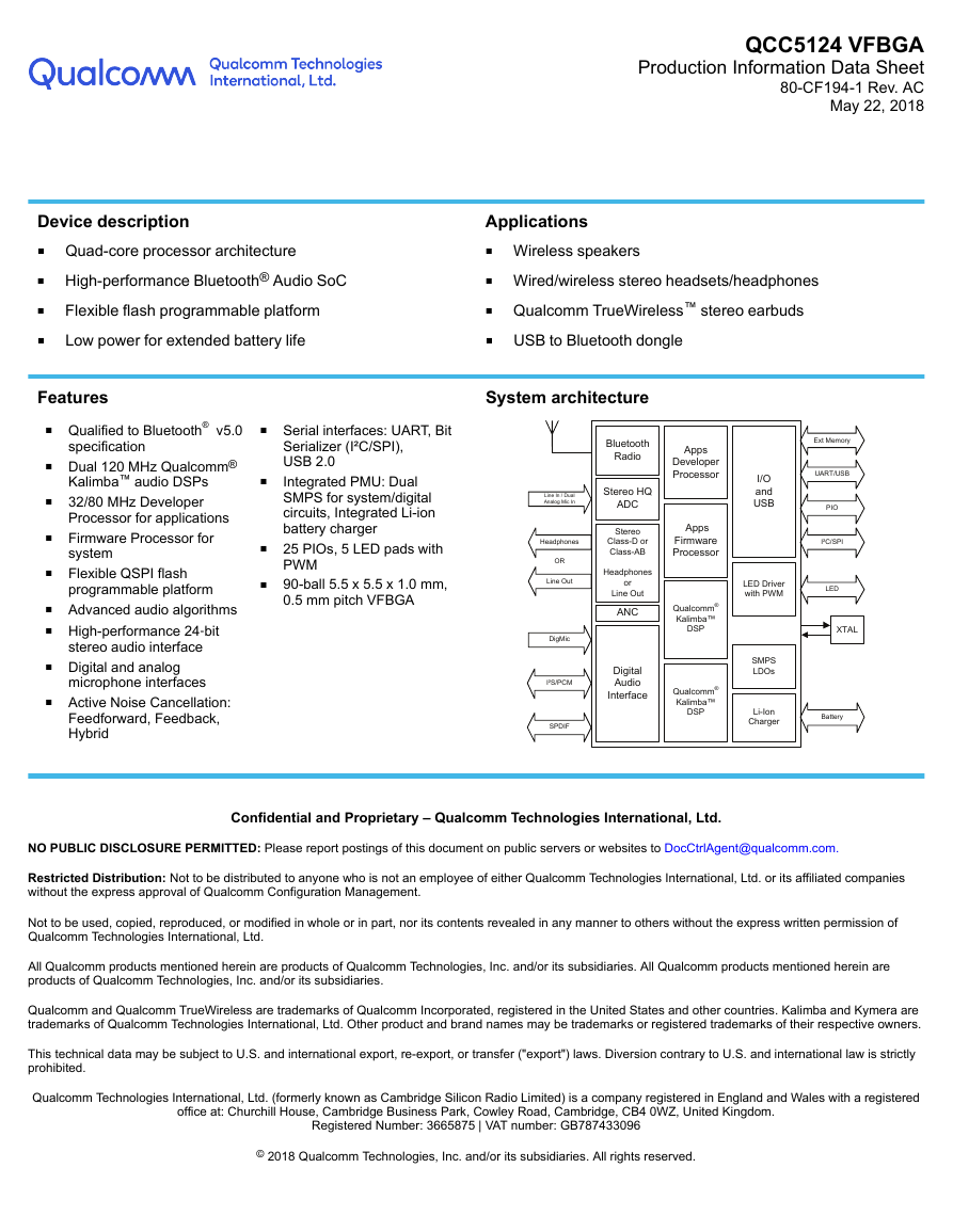
System architecture
Bluetooth
Radio
Stereo HQ
ADC
Stereo
Class-D or
Class-AB
Headphones
or
Line Out
ANC
Digital
Audio
Interface
Apps
Developer
Processor
Apps
Firmware
Processor
Qualcomm®
Kalimba™
DSP
Qualcomm®
Kalimba™
DSP
I/O
and
USB
LED Driver
with PWM
SMPS
LDOs
Li-Ion
Charger
Ext Memory
UART/USB
PIO
I²C/SPI
LED
XTAL
Battery
Line In / Dual
Analog Mic In
Headphones
OR
Line Out
DigMic
I²S/PCM
SPDIF
Device description
■ Quad-core processor architecture
■ High-performance Bluetooth® Audio SoC
■
■
Flexible flash programmable platform
Low power for extended battery life
■ Serial interfaces: UART, Bit
Serializer (I²C/SPI),
USB 2.0
Integrated PMU: Dual
SMPS for system/digital
circuits, Integrated Li-ion
battery charger
25 PIOs, 5 LED pads with
PWM
90-ball 5.5 x 5.5 x 1.0 mm,
0.5 mm pitch VFBGA
■
■
■
Features
■ Qualified to Bluetooth® v5.0
specification
■ Dual 120 MHz Qualcomm®
Kalimba™ audio DSPs
32/80 MHz Developer
Processor for applications
■
■ Firmware Processor for
system
■ Flexible QSPI flash
programmable platform
■ Advanced audio algorithms
■ High-performance 24‑bit
stereo audio interface
■ Digital and analog
microphone interfaces
■ Active Noise Cancellation:
Feedforward, Feedback,
Hybrid
Confidential and Proprietary – Qualcomm Technologies International, Ltd.
NO PUBLIC DISCLOSURE PERMITTED: Please report postings of this document on public servers or websites to DocCtrlAgent@qualcomm.com.
Restricted Distribution: Not to be distributed to anyone who is not an employee of either Qualcomm Technologies International, Ltd. or its affiliated companies
without the express approval of Qualcomm Configuration Management.
Not to be used, copied, reproduced, or modified in whole or in part, nor its contents revealed in any manner to others without the express written permission of
Qualcomm Technologies International, Ltd.
All Qualcomm products mentioned herein are products of Qualcomm Technologies, Inc. and/or its subsidiaries. All Qualcomm products mentioned herein are
products of Qualcomm Technologies, Inc. and/or its subsidiaries.
Qualcomm and Qualcomm TrueWireless are trademarks of Qualcomm Incorporated, registered in the United States and other countries. Kalimba and Kymera are
trademarks of Qualcomm Technologies International, Ltd. Other product and brand names may be trademarks or registered trademarks of their respective owners.
This technical data may be subject to U.S. and international export, re-export, or transfer ("export") laws. Diversion contrary to U.S. and international law is strictly
prohibited.
Qualcomm Technologies International, Ltd. (formerly known as Cambridge Silicon Radio Limited) is a company registered in England and Wales with a registered
office at: Churchill House, Cambridge Business Park, Cowley Road, Cambridge, CB4 0WZ, United Kingdom.
Registered Number: 3665875 | VAT number: GB787433096
© 2018 Qualcomm Technologies, Inc. and/or its subsidiaries. All rights reserved.
�
General description
QCC5124 VFBGA is a system on-chip (SoC) with on-chip Bluetooth, audio and programmable application processor.
It includes high-performance, analog, and digital audio codecs, Class-AB and Class-D headphone drivers, advanced
power management, Li-ion battery charger, light-emitting diode (LED) drivers, and flexible interfaces including inter-
integrated circuit sound (I²S), inter-integrated circuit interface (I²C), universal asynchronous receiver transmitter
(UART), and programmable input/output (PIO).
An application-dedicated Developer Processor and a system Firmware Processor run code from an external quad
serial peripheral interface (QSPI) flash. Both processors have tightly coupled memory (TCM) and an on-chip cache
for performance while executing from external flash memory. The system Firmware Processor provides functions
developed by Qualcomm Technologies International, Ltd. (QTIL). The Developer processor provides flexibility to the
product designer to customize their product.
The Audio subsystem contains two programmable Kalimba cores running Qualcomm® Kymera™ system DSP
architecture framework from read only memory (ROM). A range of audio processing capabilities are provided from
ROM which are configurable in fully flexible audio graphs. In built capabilities in ROM, may be complimented or
replaced by capabilities run from random access memory (RAM), including those provided by QTIL, the product
designer or third parties.
The flexibility provided by the fully programmable applications processor plus the ability to configure and program the
audio processors enables manufacturers to easily differentiate products with new features.
QCC5124 VFBGA is driven by a flexible, software platform with powerful integrated development environment (IDE)
support. This enables rapid time-to-market deployment for a broad range of consumer electronic products, including
headphones, headsets, speakers, and Qualcomm TrueWireless stereo earbuds.
For more information on development tools and audio development kit (ADK)s for the QCC5124 VFBGA, including
information on Bluetooth and other features supported, see createpoint.qti.qualcomm.com.
80-CF194-1 Rev. AC
Confidential and Proprietary – Qualcomm Technologies International, Ltd.
MAY CONTAIN U.S. AND INTERNATIONAL EXPORT CONTROLLED INFORMATION
2
�
Ordering information
Device
Type
Package
Size
Shipment method
Order number
QCC5124 VFBGA
VFBGA 90-ball
(Pb free)
5.5 x 5.5 x 1.0 mm
0.5 mm pitch
Tape and reel
QCC5124-0-CSP90
NOTE
Your attention is drawn to QTIL’s Terms of Supply, see http://www.qualcomm.com/salesterms or please
request a copy), in particular the section covering Product Warranties & Disclaimers. Please note that
the product warranty differs for production, pre-production, and other versions.
Production status minimum order quantity is 2 kpcs.
Supply chain: QTIL's manufacturing policy is to multisource volume products. For further details,
contact your local sales account manager or representative.
QCC5124 VFBGA Development Kit ordering information
QTIL supplies QCC5124 VFBGA development equipment.
Description
Model
QCC5124 VFBGA Development Kit
TRBI200 Transaction Bridge Interface High-
Speed Debug Adaptor and Programmer
DK-QCC5124-VFBGA90-A-0
DK-TRBI200-CE684-1
Order number
65-CF989-240
65-CE684-1
The QCC5124 VFBGA Development Kit, includes a flexible development board that has a wide range of
interconnects, and QCC5124 VFBGA mounted on a plug-in module.
TRBI200 is a high-speed universal serial bus (USB) to transaction bus interface that supports high-speed debug and
flash programming.
NOTE
TRBI200 use is not mandatory for flash programming or other manufacturing operations. Those actions
are performable using direct USB connection to the QCC5124 VFBGA USB device interface.
QTIL contacts
General information
Information on this product
Customer support for this product
Details of compliance and standards
Help with this document
www.qualcomm.com
qcsales@qti.qualcomm.com
createpoint.qti.qualcomm.com
product.compliance@qti.qualcomm.com
document.feedback@qti.qualcomm.com
80-CF194-1 Rev. AC
Confidential and Proprietary – Qualcomm Technologies International, Ltd.
MAY CONTAIN U.S. AND INTERNATIONAL EXPORT CONTROLLED INFORMATION
3
�
Device details
Li-ion battery charger
■ Integrated battery charger supporting internal mode (up to
200 mA) and external mode (up to 1.8 A)
■ Variable float (or termination) voltage adjustable in 50 mV
steps from 3.65 V to 4.4 V
■ Thermal monitoring and management are implementable
in application software
■ Pre-charge to fast charge transition configurable at 2.5 V,
2.9 V, 3.0 V, and 3.1 V
Power management
■ Integrated power management unit (PMU) to minimize
external components
■ QCC5124 VFBGA runs directly from a Li-ion, USB, or
external supply (2.8 V to 6.5 V)
■ Auto-switching between battery and USB (or other)
charging source
■ Power islands employed to optimize power consumption
for variety of use-cases
■ Dual switch-mode power supply (SMPS):
□ Automatic mode selection to minimize power
consumption
□ 1.8 V SMPS generates power for both the device and
off-chip circuits
□ Dedicated digital SMPS (output voltage changes
automatically to minimize device power consumption)
Audio subsystem
■ Dual 32‑bit Kalimba audio digital signal processor (DSP)
cores with flexible clocking from 2 MHz to 120 MHz to
allow optimization and trade-off performance vs. power
consumption
■ DSPs execute code from ROM and from program RAM,
original equipment manufacturer (OEM) and third party
developed features can run from program RAM
■ 80 KB program RAM
■ 256 KB data RAM
■ 5 Mb ROM
Application subsystem
■ Dual core application subsystem 32/80 MHz operation
■ 32‑bit Firmware Processor:
□ Reserved for system use
□ Runs Bluetooth upper stack, profiles, house-keeping
code
■ 32‑bit Developer Processor:
□ Runs developer applications
■ Both cores execute code from external flash memory using
QSPI clocked at 32 MHz or 80 MHz
■ On-chip caches per core allow for optimized performance
and power consumption
Bluetooth subsystem
■ Qualified to Bluetooth v5.0 specification including 2 Mbps
Bluetooth low energy (Production parts)
■ Single ended antenna connection with on-chip balun and
Tx/Rx switch
■ Bluetooth, Bluetooth low energy, and mixed topologies
supported
■ Class 1 support
80-CF194-1 Rev. AC
Confidential and Proprietary – Qualcomm Technologies International, Ltd.
MAY CONTAIN U.S. AND INTERNATIONAL EXPORT CONTROLLED INFORMATION
4
�
QCC5124 VFBGA Data Sheet
Device details
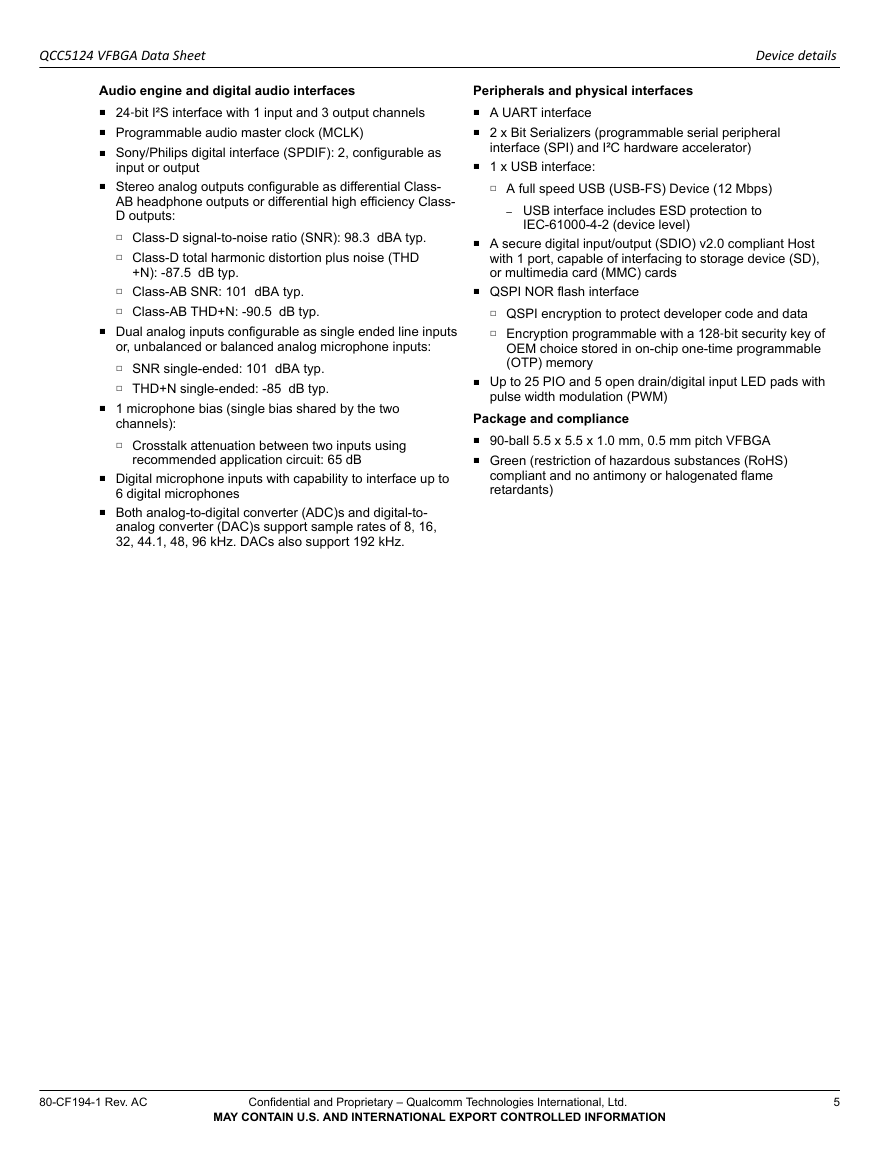
Audio engine and digital audio interfaces
■ 24‑bit I²S interface with 1 input and 3 output channels
■ Programmable audio master clock (MCLK)
■ Sony/Philips digital interface (SPDIF): 2, configurable as
input or output
■ Stereo analog outputs configurable as differential Class-
AB headphone outputs or differential high efficiency Class-
D outputs:
□ Class-D signal-to-noise ratio (SNR): 98.3 dBA typ.
□ Class-D total harmonic distortion plus noise (THD
+N): -87.5 dB typ.
□ Class-AB SNR: 101 dBA typ.
□ Class-AB THD+N: -90.5 dB typ.
■ Dual analog inputs configurable as single ended line inputs
or, unbalanced or balanced analog microphone inputs:
□ SNR single-ended: 101 dBA typ.
□ THD+N single-ended: -85 dB typ.
■ 1 microphone bias (single bias shared by the two
channels):
□ Crosstalk attenuation between two inputs using
recommended application circuit: 65 dB
■ Digital microphone inputs with capability to interface up to
6 digital microphones
■ Both analog-to-digital converter (ADC)s and digital-to-
analog converter (DAC)s support sample rates of 8, 16,
32, 44.1, 48, 96 kHz. DACs also support 192 kHz.
Peripherals and physical interfaces
■ A UART interface
■ 2 x Bit Serializers (programmable serial peripheral
interface (SPI) and I²C hardware accelerator)
■ 1 x USB interface:
□ A full speed USB (USB-FS) Device (12 Mbps)
– USB interface includes ESD protection to
IEC-61000-4-2 (device level)
■ A secure digital input/output (SDIO) v2.0 compliant Host
with 1 port, capable of interfacing to storage device (SD),
or multimedia card (MMC) cards
■ QSPI NOR flash interface
□ QSPI encryption to protect developer code and data
□ Encryption programmable with a 128‑bit security key of
OEM choice stored in on-chip one-time programmable
(OTP) memory
■ Up to 25 PIO and 5 open drain/digital input LED pads with
pulse width modulation (PWM)
Package and compliance
■ 90-ball 5.5 x 5.5 x 1.0 mm, 0.5 mm pitch VFBGA
■ Green (restriction of hazardous substances (RoHS)
compliant and no antimony or halogenated flame
retardants)
80-CF194-1 Rev. AC
Confidential and Proprietary – Qualcomm Technologies International, Ltd.
MAY CONTAIN U.S. AND INTERNATIONAL EXPORT CONTROLLED INFORMATION
5
�
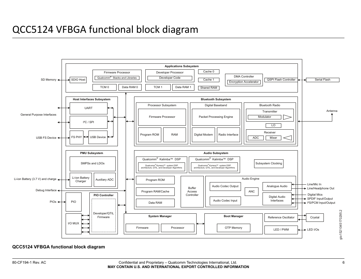
QCC5124 VFBGA functional block diagram
SD Memory
SDIO Host
Firmware Processor
Qualcomm® Stacks and Libraries
Developer Processor
Developer Code
Applications Subsystem
Cache 0
Cache 1
DMA Controller
Encryption Accelerator
QSPI Flash Controller
Serial Flash
TCM 0
Data RAM 0
TCM 1
Data RAM 1
Shared RAM
General Purpose Interfaces
Host Interfaces Subsystem
UART
I²C / SPI
Processor Subsystem
Bluetooth Subsystem
Digital Baseband
Firmware Processor
Packet Processing Engine
USB FS Device
FS PHY
USB Device
Program ROM
RAM
Digital Modem
Radio Interface
PMU Subsystem
SMPSs and LDOs
Qualcomm® Kalimba™ DSP
Qualcomm® Kalimba™ DSP
Qualcomm® Kymera™ system DSP
architecture, QTIL, and Developer Algorithms
Qualcomm® Kymera™ system DSP
architecture, QTIL, and Developer Algorithms
Audio Subsystem
Antenna
Bluetooth Radio
Transmitter
Modulator
LO
Receiver
Mixer
ADC
Subsystem Clocking
Audio Engine
Li-ion Battery (3.7 V) and charge
Li-ion Battery
Charger
Auxiliary ADC
Debug Interface
PIOs
PIO
PIO Controller
Developer/QTIL
Firmware
Program ROM
Program RAM/Cache
Data RAM
System Manager
I/O MUX
Firmware
Processor
QCC5124 VFBGA functional block diagram
Buffer
Access
Controller
Audio Codec Output
Analogue Audio
Audio Codec Input
ANC
Digital Audio
Interfaces
Line/Mic In
Line/Headphone Out
Digital Mics
SPDIF Input/Output
I²S/PCM Input/Output
Boot Manager
OTP Memory
Reference Oscillator
Crystal
LED / PWM
LED I/Os
80-CF194-1 Rev. AC
Confidential and Proprietary – Qualcomm Technologies International, Ltd.
MAY CONTAIN U.S. AND INTERNATIONAL EXPORT CONTROLLED INFORMATION
2
.
5
9
2
0
7
1
5
4
0
1
2
5
1
o
g
i
6
�
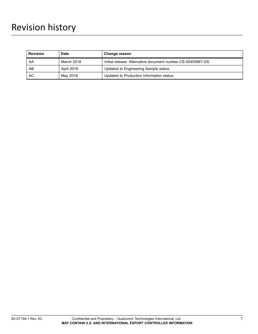
Revision history
Revision
Date
Change reason
AA
AB
AC
March 2018
April 2018
May 2018
Initial release. Alternative document number CS-00405667-DS.
Updated to Engineering Sample status.
Updated to Production Information status.
80-CF194-1 Rev. AC
Confidential and Proprietary – Qualcomm Technologies International, Ltd.
MAY CONTAIN U.S. AND INTERNATIONAL EXPORT CONTROLLED INFORMATION
7
�
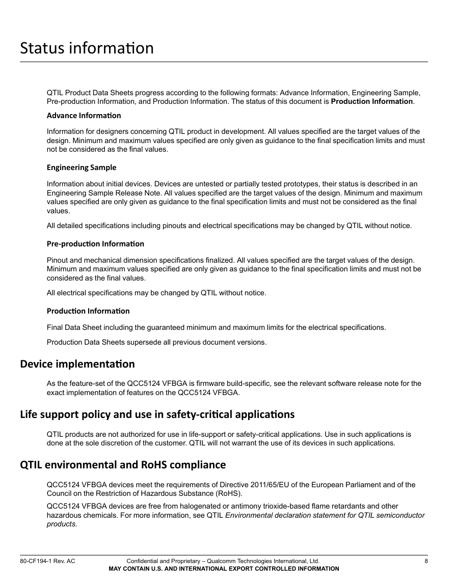
Status information
QTIL Product Data Sheets progress according to the following formats: Advance Information, Engineering Sample,
Pre-production Information, and Production Information. The status of this document is Production Information.
Advance Information
Information for designers concerning QTIL product in development. All values specified are the target values of the
design. Minimum and maximum values specified are only given as guidance to the final specification limits and must
not be considered as the final values.
Engineering Sample
Information about initial devices. Devices are untested or partially tested prototypes, their status is described in an
Engineering Sample Release Note. All values specified are the target values of the design. Minimum and maximum
values specified are only given as guidance to the final specification limits and must not be considered as the final
values.
All detailed specifications including pinouts and electrical specifications may be changed by QTIL without notice.
Pre-production Information
Pinout and mechanical dimension specifications finalized. All values specified are the target values of the design.
Minimum and maximum values specified are only given as guidance to the final specification limits and must not be
considered as the final values.
All electrical specifications may be changed by QTIL without notice.
Production Information
Final Data Sheet including the guaranteed minimum and maximum limits for the electrical specifications.
Production Data Sheets supersede all previous document versions.
Device implementation
As the feature-set of the QCC5124 VFBGA is firmware build-specific, see the relevant software release note for the
exact implementation of features on the QCC5124 VFBGA.
Life support policy and use in safety-critical applications
QTIL products are not authorized for use in life-support or safety-critical applications. Use in such applications is
done at the sole discretion of the customer. QTIL will not warrant the use of its devices in such applications.
QTIL environmental and RoHS compliance
QCC5124 VFBGA devices meet the requirements of Directive 2011/65/EU of the European Parliament and of the
Council on the Restriction of Hazardous Substance (RoHS).
QCC5124 VFBGA devices are free from halogenated or antimony trioxide-based flame retardants and other
hazardous chemicals. For more information, see QTIL Environmental declaration statement for QTIL semiconductor
products.
80-CF194-1 Rev. AC
Confidential and Proprietary – Qualcomm Technologies International, Ltd.
MAY CONTAIN U.S. AND INTERNATIONAL EXPORT CONTROLLED INFORMATION
8
�


 2023年江西萍乡中考道德与法治真题及答案.doc
 2012年重庆南川中考生物真题及答案.doc
 2013年江西师范大学地理学综合及文艺理论基础考研真题.doc
 2020年四川甘孜小升初语文真题及答案I卷.doc
 2020年注册岩土工程师专业基础考试真题及答案.doc
 2023-2024学年福建省厦门市九年级上学期数学月考试题及答案.doc
 2021-2022学年辽宁省沈阳市大东区九年级上学期语文期末试题及答案.doc
 2022-2023学年北京东城区初三第一学期物理期末试卷及答案.doc
 2018上半年江西教师资格初中地理学科知识与教学能力真题及答案.doc
 2012年河北国家公务员申论考试真题及答案-省级.doc
 2020-2021学年江苏省扬州市江都区邵樊片九年级上学期数学第一次质量检测试题及答案.doc
 2022下半年黑龙江教师资格证中学综合素质真题及答案.doc