logo资料库

使用Altera的FPGA内核建立PCI/PXI接口.pdf

第1页 / 共368页
第2页 / 共368页
第3页 / 共368页
第4页 / 共368页
第5页 / 共368页
第6页 / 共368页
第7页 / 共368页
第8页 / 共368页
资料共368页,剩余部分请下载后查看
PCI Compiler
User Guide
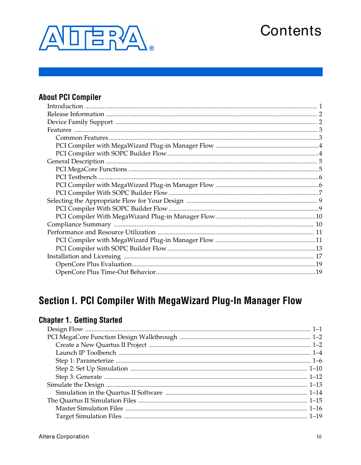
Contents
About PCI Compiler
Introduction
Release Information
Device Family Support
Features
Common Features
PCI Compiler with MegaWizard Plug-in Manager Flow
PCI Compiler with SOPC Builder Flow
General Description
PCI MegaCore Functions
PCI Testbench
PCI Compiler with MegaWizard Plug-in Manager Flow
PCI Compiler With SOPC Builder Flow
Selecting the Appropriate Flow for Your Design
PCI Compiler With SOPC Builder Flow
Advantages
Disadvantages
PCI Compiler With MegaWizard Plug-in Manager Flow
Advantages
Disadvantages
Compliance Summary
Performance and Resource Utilization
PCI Compiler with MegaWizard Plug-in Manager Flow
PCI Compiler with SOPC Builder Flow
Installation and Licensing
OpenCore Plus Evaluation
OpenCore Plus Time-Out Behavior
Section I. PCI Compiler With MegaWizard Plug-In Manager Flow
1. Getting Started
Design Flow
PCI MegaCore Function Design Walkthrough
Create a New Quartus II Project
Launch IP Toolbench
Step 1: Parameterize
Step 2: Set Up Simulation
Step 3: Generate
Simulate the Design
Simulation in the Quartus II Software
The Quartus II Simulation Files
Master Simulation Files
Target Simulation Files
Compile the Design
Program a Device
PCI Timing Support
Using the Reference Designs
pci_mt32 MegaCore Function Reference Design
Synthesis & Compilation Instructions
pci_mt64 MegaCore Function Reference Design
synthesis & Compilation Instructions
2. Parameter Settings
Parameterize PCI Compiler
PCI MegaCore Function Settings
Read-Only PCI Configuration Registers
PCI Base Address Registers (BARs)
Advanced PCI MegaCore Function Features
Optional Registers
Optional Interrupt Capabilities
Master Features
Allow Variable Byte Enables During Burst Transaction
Use in Host Bridge Application
Allow Internal Arbitration Logic
Disable Master Latency Timer
Assume ack64n Response
Variation File Parameters
3. Functional Description
Functional Overview
Target Device Signals & Signal Assertion
Master Device Signals & Signal Assertion
PCI Bus Signals
Parameterized Configuration Register Signals
Local Address, Data, Command, & Byte Enable Signals
Target Local-Side Signals
Master Local-Side Signals
PCI Bus Commands
Configuration Registers
Vendor ID Register
Device ID Register
Command Register
Status Register
Revision ID Register
Class Code Register
Cache Line Size Register
Latency Timer Register
Header Type Register
Base Address Registers
CardBus CIS Pointer Register
Subsystem Vendor ID Register
Subsystem ID Register
Expansion ROM Base Address Register
Capabilities Pointer
Interrupt Line Register
Interrupt Pin Register
Minimum Grant Register
Maximum Latency Register
Target Mode Operation
Target Read Transactions
Memory Read Transactions
Single-cycle Memory Read Target Transactions
Burst Memory Read Target Transactions
Mismatched Bus Width Memory Read Target Transactions
I/O Read Transactions
Configuration Read Transactions
Target Write Transactions
Memory Write Transactions
Single-cycle Memory Write Target Transactions
Burst Memory Write Target Transactions
Mismatched Bus-Width Memory Write Target Transactions
I/O Write Transactions
Configuration Write Transactions
Target Transaction Terminations
Retry
Disconnect
Target Abort
Additional Design Guidelines for Target Transactions
Master Mode Operation
PCI Bus Parking
Design Consideration
Master Read Transactions
Memory Read Transactions
Burst Memory Read Master Transactions
Single-Cycle Memory Read Master Transaction
Mismatched Bus Width Burst Memory Read Master Transactions
I/O & Configuration Read Transactions
Master Write Transactions
Memory Write Transactions
Burst Memory Write Master Transactions
Burst Memory Write Master Transactions with Variable Byte Enables
32-Bit Single-Cycle Memory Write Master Transactions
64-Bit Single Cycle Memory Write Master Transactions
Mismatched Bus Width Burst Memory Write Master Transactions
I/O & Configuration Write Master Transactions
Abnormal Master Transaction Termination
Latency Timer Expires
Retry
Disconnect Without Data
Disconnect with Data
Target Abort
Master Abort
Host Bridge Operation
Using the PCI MegaCore Function as a Host Bridge
PCI Configuration Read Transaction from the pci_mt64 Local Master Device to the Internal Configuration Space
PCI Configuration Write Transaction from the pci_mt64 Local Master Device to the Internal Configuration Space
64-Bit Addressing, Dual Address Cycle (DAC)
Target Mode Operation
64-Bit Address, 64-Bit Data Single-Cycle Target Read Transaction
Master Mode Operation
64-Bit Address, 64-Bit Data Master Burst Memory Read Transaction
4. Testbench
General Description
Features
PCI Testbench Files
Testbench Specifications
Master Transactor (mstr_tranx)
PROCEDURES and TASKS Sections
INITIALIZATION Section
USER COMMANDS Section
cfg_rd
cfg_wr
mem_wr_32
mem_rd_32
mem_wr_64
mem_rd_64
io_wr
io_rd
Target Transactor (trgt_tranx)
FILE IO section
PROCEDURES and TASKS sections
Bus Monitor (monitor)
Clock Generator (clk_gen)
Arbiter (arbiter)
Pull Up (pull_up)
Local Reference Design
Local Target
DMA Engine
Local Master
lm_lastn Generator
Prefetch
LPM RAM
Simulation Flow
Section II. PCI Compiler With SOPC Builder Flow
5. Getting Started
Design Flow
PCI Compiler with SOPC Builder Flow Design Walkthrough
Create a New Quartus II Project
Set Up the PCI-Avalon Bridge
Add the Remaining Components to the SOPC Builder System
Complete the Connections in SOPC Builder
Generate the SOPC Builder System
Files Generated by SOPC Builder
Simulate the Design
Compile the Design
Program a Device
Upgrading Systems from a Previous Version
6. Parameter Settings
System Options-1
PCI Device Mode
PCI Master/Target Peripheral
PCI Target-Only Peripheral
PCI Host-Bridge Device
PCI Target Performance
Single-Cycle Transfers Only
Burst Transfers with Single Pending Read
Burst Transfers with Multiple Pending Reads
Maximum Target Read Burst Size
PCI Master Performance
Burst Transfers with Single Pending Read
Burst Transfers with Multiple Pending Reads
Value of Multiple Pending Reads
System Options-2
PCI Bus Speed
PCI Global Reset Signal
PCI Data Bus Width
Clock Domains
PCI Bus Arbiter
PCI Configuration
PCI Base Address Registers
PCI Read-Only Registers
Setting the PCI Base Address Register Values
Manual Setting of the BAR Size & Avalon Base Address
Avalon Configuration
7. Functional Description
Functional Overview
PCI-Avalon Bridge Blocks
Avalon-MM Ports
Prefetchable Avalon-MM Master
Non-Prefetchable Avalon-MM Master
PCI Bus Access Slave
Control Register Access Avalon-MM Slave
Control/Status Register Module
Mailbox Registers
PCI MegaCore Function
PCI Bus Arbiter
Other PCI-Avalon Bridge Modules
PCI Operational Modes
PCI Target-Only Peripheral Mode Operation
PCI Master/Target Peripheral Mode Operation
Control Register Access Avalon Slave
PCI Host-Bridge Device Mode Operation
Performance Profiles
Target Performance
Single-Cycle Transfers Only
Burst Transfers With Single Pending Read
Burst Transfers With Multiple Pending Reads
Master Performance
Burst Transfers With Single Pending Read
Burst Transfers With Multiple Pending Reads
Interface Signals
PCI Bus Arbiter Signals
PCI Bus Commands
PCI Target Operation
Non-Prefetchable Operations
Non-Prefetchable Write Operations
I/O Write Operations
Non-Prefetchable Read Operations
Prefetchable Operations
Prefetchable Write Operations
Prefetchable Read Operations
PCI-to-Avalon Address Translation
PCI Master Operation
Avalon-To-PCI Read & Write Operation
Avalon-to-PCI Write Requests
Avalon-to-PCI Read Requests
Arbitration Among Pending PCI Master Requests
Avalon-to-PCI Address Translation
Ordering of Requests
Ordering of Avalon-to-PCI Operations
Ordering PCI-to-Avalon Operations
PCI Host-Bridge Operation
Altera-Provided PCI Bus Arbiter
Interrupts
Generation of PCI Interrupts
Reception of PCI Interrupts
Generation of Avalon-MM Interrupts
Control & Status Registers
PCI Interrupt Status Register
PCI Interrupt Enable Register
PCI Mailbox Register Access
Avalon-to-PCI Address Translation Table
Read-Only Configuration Registers
Avalon-MM Interrupt Status Register
Avalon-MM Interrupt Enable Register
Avalon Mailbox Register Access
8. Testbench
General Description
Features
PCI Testbench Files
Testbench Specifications
Master Transactor (mstr_tranx)
PROCEDURES and TASKS Sections
INITIALIZATION Section
USER COMMANDS Section
cfg_rd
cfg_wr
mem_wr_32
mem_rd_32
mem_wr_64
mem_rd_64
io_wr
io_rd
Target Transactor (trgt_tranx)
FILE IO section
PROCEDURES and TASKS sections
Bus Monitor (monitor)
Arbiter (arbiter)
Pull Up (pull_up)
Simulation Flow
Appendix A. Using PCI Constraint File Tcl Scripts
Introduction
PCI Constraint Files
Simultaneous Switching Noise (SSN) Considerations
Additional Options
-speed
-no_compile
-no_pinouts
-pin_prefix
-pin_suffix
-help
Upgrading Assignments from a Previous Version of PCI Compiler
Upgrading PCI Assignments Containing Nondefault PCI Pin Names
How to Contact Altera
Typographic Conventions
PCI Compiler User Guide 101 Innovation Drive San Jose, CA 95134 www.altera.com Compiler Version: Document Date: 8.0 May 2008
Copyright © 2008 Altera Corporation. All rights reserved. Altera, The Programmable Solutions Company, the stylized Altera logo, specific device des- ignations, and all other words and logos that are identified as trademarks and/or service marks are, unless noted otherwise, the trademarks and service marks of Altera Corporation in the U.S. and other countries. All other product or service names are the property of their respective holders. Al- tera products are protected under numerous U.S. and foreign patents and pending applications, maskwork rights, and copyrights. Altera warrants performance of its semiconductor products to current specifications in accordance with Altera's standard warranty, but reserves the right to make changes to any products and services at any time without notice. Altera assumes no responsibility or liability arising out of the ap- plication or use of any information, product, or service described herein except as expressly agreed to in writing by Altera Corporation. Altera customers are advised to obtain the latest version of device specifications before relying on any published in- formation and before placing orders for products or services. Printed on recycled paper ii UG-PCICOMPILER-4.6 Altera Corporation
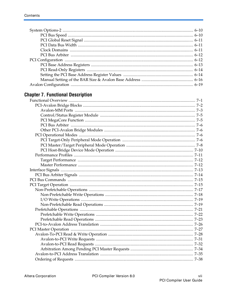
Contents About PCI Compiler Introduction ................................................................................................................................................ 1 Release Information ................................................................................................................................... 2 Device Family Support ............................................................................................................................. 2 Features ....................................................................................................................................................... 3 Common Features ..................................................................................................................................3 PCI Compiler with MegaWizard Plug-in Manager Flow ................................................................4 PCI Compiler with SOPC Builder Flow..............................................................................................4 General Description ................................................................................................................................... 5 PCI MegaCore Functions ......................................................................................................................5 PCI Testbench .........................................................................................................................................6 PCI Compiler with MegaWizard Plug-in Manager Flow ................................................................6 PCI Compiler With SOPC Builder Flow .............................................................................................7 Selecting the Appropriate Flow for Your Design ................................................................................. 9 PCI Compiler With SOPC Builder Flow .............................................................................................9 PCI Compiler With MegaWizard Plug-in Manager Flow..............................................................10 Compliance Summary ............................................................................................................................ 10 Performance and Resource Utilization ................................................................................................. 11 PCI Compiler with MegaWizard Plug-in Manager Flow ..............................................................11 PCI Compiler with SOPC Builder Flow............................................................................................13 Installation and Licensing ...................................................................................................................... 17 OpenCore Plus Evaluation..................................................................................................................19 OpenCore Plus Time-Out Behavior...................................................................................................19 Section I. PCI Compiler With MegaWizard Plug-In Manager Flow Chapter 1. Getting Started Design Flow ............................................................................................................................................ 1–1 PCI MegaCore Function Design Walkthrough ................................................................................. 1–2 Create a New Quartus II Project .................................................................................................... 1–2 Launch IP Toolbench ....................................................................................................................... 1–4 Step 1: Parameterize ......................................................................................................................... 1–6 Step 2: Set Up Simulation .............................................................................................................. 1–10 Step 3: Generate .............................................................................................................................. 1–12 Simulate the Design ............................................................................................................................. 1–13 Simulation in the Quartus II Software ........................................................................................ 1–14 The Quartus II Simulation Files ......................................................................................................... 1–15 Master Simulation Files ................................................................................................................. 1–16 Target Simulation Files .................................................................................................................. 1–19 Altera Corporation iii
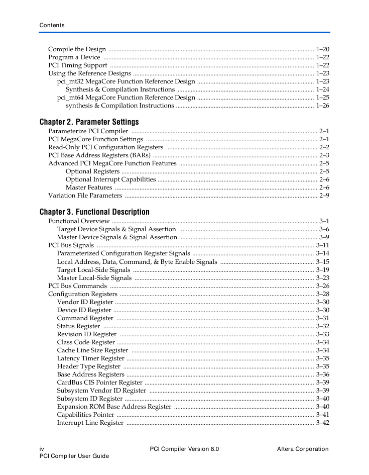
Contents Compile the Design ............................................................................................................................. 1–20 Program a Device ................................................................................................................................ 1–22 PCI Timing Support ............................................................................................................................ 1–22 Using the Reference Designs .............................................................................................................. 1–23 pci_mt32 MegaCore Function Reference Design ....................................................................... 1–23 Synthesis & Compilation Instructions ................................................................................... 1–24 pci_mt64 MegaCore Function Reference Design ....................................................................... 1–25 synthesis & Compilation Instructions .................................................................................... 1–26 Chapter 2. Parameter Settings Parameterize PCI Compiler ................................................................................................................. 2–1 PCI MegaCore Function Settings ........................................................................................................ 2–1 Read-Only PCI Configuration Registers ............................................................................................ 2–2 PCI Base Address Registers (BARs) .................................................................................................... 2–3 Advanced PCI MegaCore Function Features .................................................................................... 2–5 Optional Registers ....................................................................................................................... 2–5 Optional Interrupt Capabilities ................................................................................................. 2–6 Master Features ........................................................................................................................... 2–6 Variation File Parameters ..................................................................................................................... 2–9 Chapter 3. Functional Description Functional Overview ............................................................................................................................. 3–1 Target Device Signals & Signal Assertion .................................................................................... 3–6 Master Device Signals & Signal Assertion .................................................................................... 3–9 PCI Bus Signals .................................................................................................................................... 3–11 Parameterized Configuration Register Signals .......................................................................... 3–14 Local Address, Data, Command, & Byte Enable Signals ......................................................... 3–15 Target Local-Side Signals .............................................................................................................. 3–19 Master Local-Side Signals ............................................................................................................. 3–23 PCI Bus Commands ............................................................................................................................ 3–26 Configuration Registers ...................................................................................................................... 3–28 Vendor ID Register ......................................................................................................................... 3–30 Device ID Register .......................................................................................................................... 3–30 Command Register ........................................................................................................................ 3–31 Status Register ................................................................................................................................ 3–32 Revision ID Register ...................................................................................................................... 3–33 Class Code Register ........................................................................................................................ 3–34 Cache Line Size Register ............................................................................................................... 3–34 Latency Timer Register .................................................................................................................. 3–35 Header Type Register .................................................................................................................... 3–35 Base Address Registers .................................................................................................................. 3–36 CardBus CIS Pointer Register ....................................................................................................... 3–39 Subsystem Vendor ID Register .................................................................................................... 3–39 Subsystem ID Register ................................................................................................................... 3–40 Expansion ROM Base Address Register ..................................................................................... 3–40 Capabilities Pointer ........................................................................................................................ 3–41 Interrupt Line Register .................................................................................................................. 3–42 iv PCI Compiler User Guide PCI Compiler Version 8.0 Altera Corporation
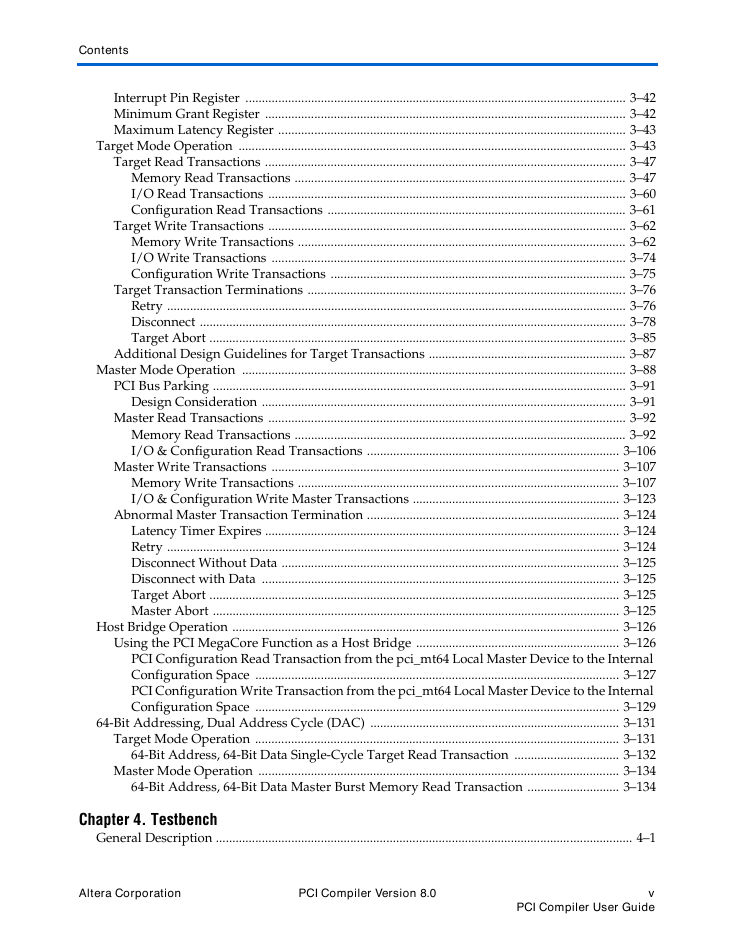
Contents Interrupt Pin Register .................................................................................................................... 3–42 Minimum Grant Register .............................................................................................................. 3–42 Maximum Latency Register .......................................................................................................... 3–43 Target Mode Operation ...................................................................................................................... 3–43 Target Read Transactions .............................................................................................................. 3–47 Memory Read Transactions ..................................................................................................... 3–47 I/O Read Transactions ............................................................................................................. 3–60 Configuration Read Transactions ........................................................................................... 3–61 Target Write Transactions ............................................................................................................. 3–62 Memory Write Transactions .................................................................................................... 3–62 I/O Write Transactions ............................................................................................................ 3–74 Configuration Write Transactions .......................................................................................... 3–75 Target Transaction Terminations ................................................................................................. 3–76 Retry ............................................................................................................................................ 3–76 Disconnect .................................................................................................................................. 3–78 Target Abort ............................................................................................................................... 3–85 Additional Design Guidelines for Target Transactions ............................................................ 3–87 Master Mode Operation ..................................................................................................................... 3–88 PCI Bus Parking .............................................................................................................................. 3–91 Design Consideration ............................................................................................................... 3–91 Master Read Transactions ............................................................................................................. 3–92 Memory Read Transactions ..................................................................................................... 3–92 I/O & Configuration Read Transactions ............................................................................. 3–106 Master Write Transactions .......................................................................................................... 3–107 Memory Write Transactions .................................................................................................. 3–107 I/O & Configuration Write Master Transactions ............................................................... 3–123 Abnormal Master Transaction Termination ............................................................................. 3–124 Latency Timer Expires ............................................................................................................ 3–124 Retry .......................................................................................................................................... 3–124 Disconnect Without Data ....................................................................................................... 3–125 Disconnect with Data ............................................................................................................. 3–125 Target Abort ............................................................................................................................. 3–125 Master Abort ............................................................................................................................ 3–125 Host Bridge Operation ...................................................................................................................... 3–126 Using the PCI MegaCore Function as a Host Bridge .............................................................. 3–126 PCI Configuration Read Transaction from the pci_mt64 Local Master Device to the Internal Configuration Space ............................................................................................................... 3–127 PCI Configuration Write Transaction from the pci_mt64 Local Master Device to the Internal Configuration Space ............................................................................................................... 3–129 64-Bit Addressing, Dual Address Cycle (DAC) ............................................................................ 3–131 Target Mode Operation ............................................................................................................... 3–131 64-Bit Address, 64-Bit Data Single-Cycle Target Read Transaction ................................ 3–132 Master Mode Operation .............................................................................................................. 3–134 64-Bit Address, 64-Bit Data Master Burst Memory Read Transaction ............................ 3–134 Chapter 4. Testbench General Description ............................................................................................................................... 4–1 Altera Corporation PCI Compiler Version 8.0 v PCI Compiler User Guide
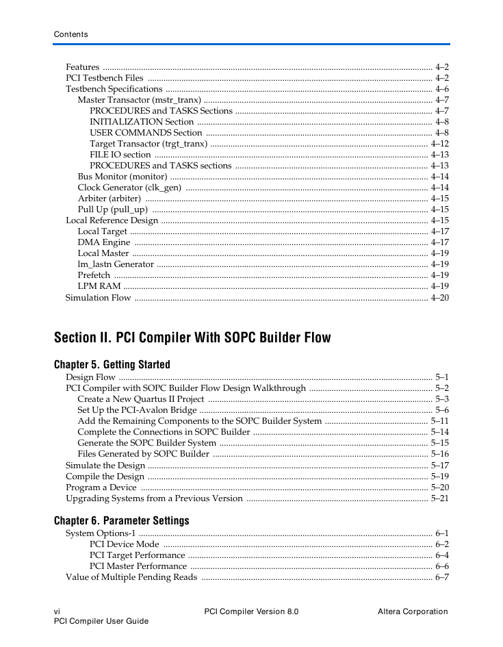
Contents Features ................................................................................................................................................... 4–2 PCI Testbench Files ............................................................................................................................... 4–2 Testbench Specifications ....................................................................................................................... 4–6 Master Transactor (mstr_tranx) ...................................................................................................... 4–7 PROCEDURES and TASKS Sections ........................................................................................ 4–7 INITIALIZATION Section ......................................................................................................... 4–8 USER COMMANDS Section ..................................................................................................... 4–8 Target Transactor (trgt_tranx) ................................................................................................. 4–12 FILE IO section .......................................................................................................................... 4–13 PROCEDURES and TASKS sections ...................................................................................... 4–13 Bus Monitor (monitor) ................................................................................................................... 4–14 Clock Generator (clk_gen) ............................................................................................................ 4–14 Arbiter (arbiter) .............................................................................................................................. 4–15 Pull Up (pull_up) ........................................................................................................................... 4–15 Local Reference Design ....................................................................................................................... 4–15 Local Target ..................................................................................................................................... 4–17 DMA Engine ................................................................................................................................... 4–17 Local Master .................................................................................................................................... 4–19 lm_lastn Generator ......................................................................................................................... 4–19 Prefetch ............................................................................................................................................ 4–19 LPM RAM ........................................................................................................................................ 4–19 Simulation Flow ................................................................................................................................... 4–20 Section II. PCI Compiler With SOPC Builder Flow Chapter 5. Getting Started Design Flow ............................................................................................................................................ 5–1 PCI Compiler with SOPC Builder Flow Design Walkthrough ....................................................... 5–2 Create a New Quartus II Project .................................................................................................... 5–3 Set Up the PCI-Avalon Bridge ........................................................................................................ 5–6 Add the Remaining Components to the SOPC Builder System .............................................. 5–11 Complete the Connections in SOPC Builder .............................................................................. 5–14 Generate the SOPC Builder System ............................................................................................. 5–15 Files Generated by SOPC Builder ................................................................................................ 5–16 Simulate the Design ............................................................................................................................. 5–17 Compile the Design ............................................................................................................................. 5–19 Program a Device ................................................................................................................................ 5–20 Upgrading Systems from a Previous Version ................................................................................. 5–21 Chapter 6. Parameter Settings System Options-1 ................................................................................................................................... 6–1 PCI Device Mode ........................................................................................................................ 6–2 PCI Target Performance ............................................................................................................. 6–4 PCI Master Performance ............................................................................................................ 6–6 Value of Multiple Pending Reads ....................................................................................................... 6–7 vi PCI Compiler User Guide PCI Compiler Version 8.0 Altera Corporation
Contents System Options-2 ................................................................................................................................. 6–10 PCI Bus Speed ............................................................................................................................ 6–10 PCI Global Reset Signal ............................................................................................................ 6–11 PCI Data Bus Width .................................................................................................................. 6–11 Clock Domains .......................................................................................................................... 6–11 PCI Bus Arbiter ......................................................................................................................... 6–12 PCI Configuration ............................................................................................................................... 6–12 PCI Base Address Registers ..................................................................................................... 6–13 PCI Read-Only Registers ......................................................................................................... 6–14 Setting the PCI Base Address Register Values ..................................................................... 6–14 Manual Setting of the BAR Size & Avalon Base Address ................................................... 6–16 Avalon Configuration ......................................................................................................................... 6–19 Chapter 7. Functional Description Functional Overview ............................................................................................................................. 7–1 PCI-Avalon Bridge Blocks ............................................................................................................... 7–2 Avalon-MM Ports ....................................................................................................................... 7–3 Control/Status Register Module .............................................................................................. 7–5 PCI MegaCore Function ............................................................................................................. 7–5 PCI Bus Arbiter ........................................................................................................................... 7–6 Other PCI-Avalon Bridge Modules .......................................................................................... 7–6 PCI Operational Modes ................................................................................................................... 7–6 PCI Target-Only Peripheral Mode Operation ........................................................................ 7–6 PCI Master/Target Peripheral Mode Operation .................................................................... 7–8 PCI Host-Bridge Device Mode Operation ............................................................................. 7–10 Performance Profiles ...................................................................................................................... 7–11 Target Performance .................................................................................................................. 7–12 Master Performance .................................................................................................................. 7–12 Interface Signals ................................................................................................................................... 7–13 PCI Bus Arbiter Signals ................................................................................................................. 7–14 PCI Bus Commands ............................................................................................................................ 7–15 PCI Target Operation .......................................................................................................................... 7–15 Non-Prefetchable Operations ....................................................................................................... 7–17 Non-Prefetchable Write Operations ....................................................................................... 7–18 I/O Write Operations ............................................................................................................... 7–19 Non-Prefetchable Read Operations ........................................................................................ 7–19 Prefetchable Operations ................................................................................................................ 7–21 Prefetchable Write Operations ................................................................................................ 7–22 Prefetchable Read Operations ................................................................................................. 7–23 PCI-to-Avalon Address Translation ............................................................................................ 7–26 PCI Master Operation ......................................................................................................................... 7–27 Avalon-To-PCI Read & Write Operation .................................................................................... 7–28 Avalon-to-PCI Write Requests ................................................................................................ 7–31 Avalon-to-PCI Read Requests ................................................................................................. 7–32 Arbitration Among Pending PCI Master Requests .............................................................. 7–34 Avalon-to-PCI Address Translation ............................................................................................ 7–35 Ordering of Requests ..................................................................................................................... 7–38 Altera Corporation PCI Compiler Version 8.0 vii PCI Compiler User Guide
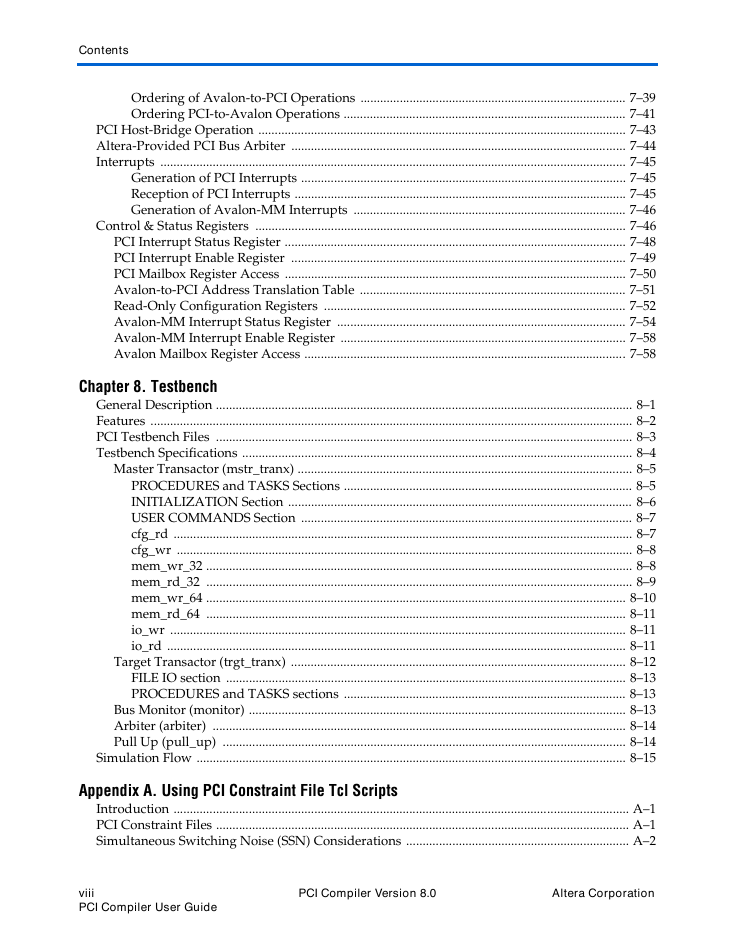
Contents Ordering of Avalon-to-PCI Operations ................................................................................. 7–39 Ordering PCI-to-Avalon Operations ...................................................................................... 7–41 PCI Host-Bridge Operation ................................................................................................................ 7–43 Altera-Provided PCI Bus Arbiter ...................................................................................................... 7–44 Interrupts .............................................................................................................................................. 7–45 Generation of PCI Interrupts ................................................................................................... 7–45 Reception of PCI Interrupts ..................................................................................................... 7–45 Generation of Avalon-MM Interrupts ................................................................................... 7–46 Control & Status Registers ................................................................................................................. 7–46 PCI Interrupt Status Register ........................................................................................................ 7–48 PCI Interrupt Enable Register ...................................................................................................... 7–49 PCI Mailbox Register Access ........................................................................................................ 7–50 Avalon-to-PCI Address Translation Table ................................................................................. 7–51 Read-Only Configuration Registers ............................................................................................ 7–52 Avalon-MM Interrupt Status Register ........................................................................................ 7–54 Avalon-MM Interrupt Enable Register ....................................................................................... 7–58 Avalon Mailbox Register Access .................................................................................................. 7–58 Chapter 8. Testbench General Description ............................................................................................................................... 8–1 Features ................................................................................................................................................... 8–2 PCI Testbench Files ............................................................................................................................... 8–3 Testbench Specifications ....................................................................................................................... 8–4 Master Transactor (mstr_tranx) ...................................................................................................... 8–5 PROCEDURES and TASKS Sections ........................................................................................ 8–5 INITIALIZATION Section ......................................................................................................... 8–6 USER COMMANDS Section ..................................................................................................... 8–7 cfg_rd ............................................................................................................................................ 8–7 cfg_wr ........................................................................................................................................... 8–8 mem_wr_32 .................................................................................................................................. 8–8 mem_rd_32 .................................................................................................................................. 8–9 mem_wr_64 ................................................................................................................................ 8–10 mem_rd_64 ................................................................................................................................ 8–11 io_wr ........................................................................................................................................... 8–11 io_rd ............................................................................................................................................ 8–11 Target Transactor (trgt_tranx) ...................................................................................................... 8–12 FILE IO section .......................................................................................................................... 8–13 PROCEDURES and TASKS sections ...................................................................................... 8–13 Bus Monitor (monitor) ................................................................................................................... 8–13 Arbiter (arbiter) .............................................................................................................................. 8–14 Pull Up (pull_up) ........................................................................................................................... 8–14 Simulation Flow ................................................................................................................................... 8–15 Appendix A. Using PCI Constraint File Tcl Scripts Introduction ........................................................................................................................................... A–1 PCI Constraint Files .............................................................................................................................. A–1 Simultaneous Switching Noise (SSN) Considerations .................................................................... A–2 viii PCI Compiler User Guide PCI Compiler Version 8.0 Altera Corporation
分享到:
收藏