Introduction to the Altera
Nios II Soft Processor
For Quartus II 11.1
1
Introduction
This tutorial presents an introduction to Altera’s Nios® II processor, which is a soft processor that can be instantiated
on an Altera FPGA device. It describes the basic architecture of Nios II and its instruction set. The Nios II processor
and its associated memory and peripheral components are easily instantiated by using Altera’s SOPC Builder or
Qsys tool in conjuction with the Quartus® II software.
A full desciption of the Nios II processor is provided in the Nios II Processor Reference Handbook, which is available
in the literature section of the Altera web site. Introductions to the SOPC Builder and Qsys tools are given in the
tutorials Introduction to the Altera SOPC Builder and Introduction to the Altera Qsys Tool, respectively. Both can
be found in the University Program section of the web site.
Contents:
• Nios II System
• Overview of Nios II Processor Features
• Register Structure
• Accessing Memory and I/O Devices
• Addressing
• Instruction Set
• Assembler Directives
• Example Program
• Exception Processing
• Cache Memory
• Tightly Coupled Memory
Altera Corporation - University Program
August 2011
1
�
INTRODUCTION TO THE ALTERA NIOS II SOFT PROCESSOR
For Quartus II 11.1
2 Background
Altera’s Nios II is a soft processor, defined in a hardware description language, which can be implemented in
Altera’s FPGA devices by using the Quartus® II CAD system. This tutorial provides a basic introduction to the Nios
II processor, intended for a user who wishes to implement a Nios II based system on an Altera Development and
Education board.
3 Nios II System
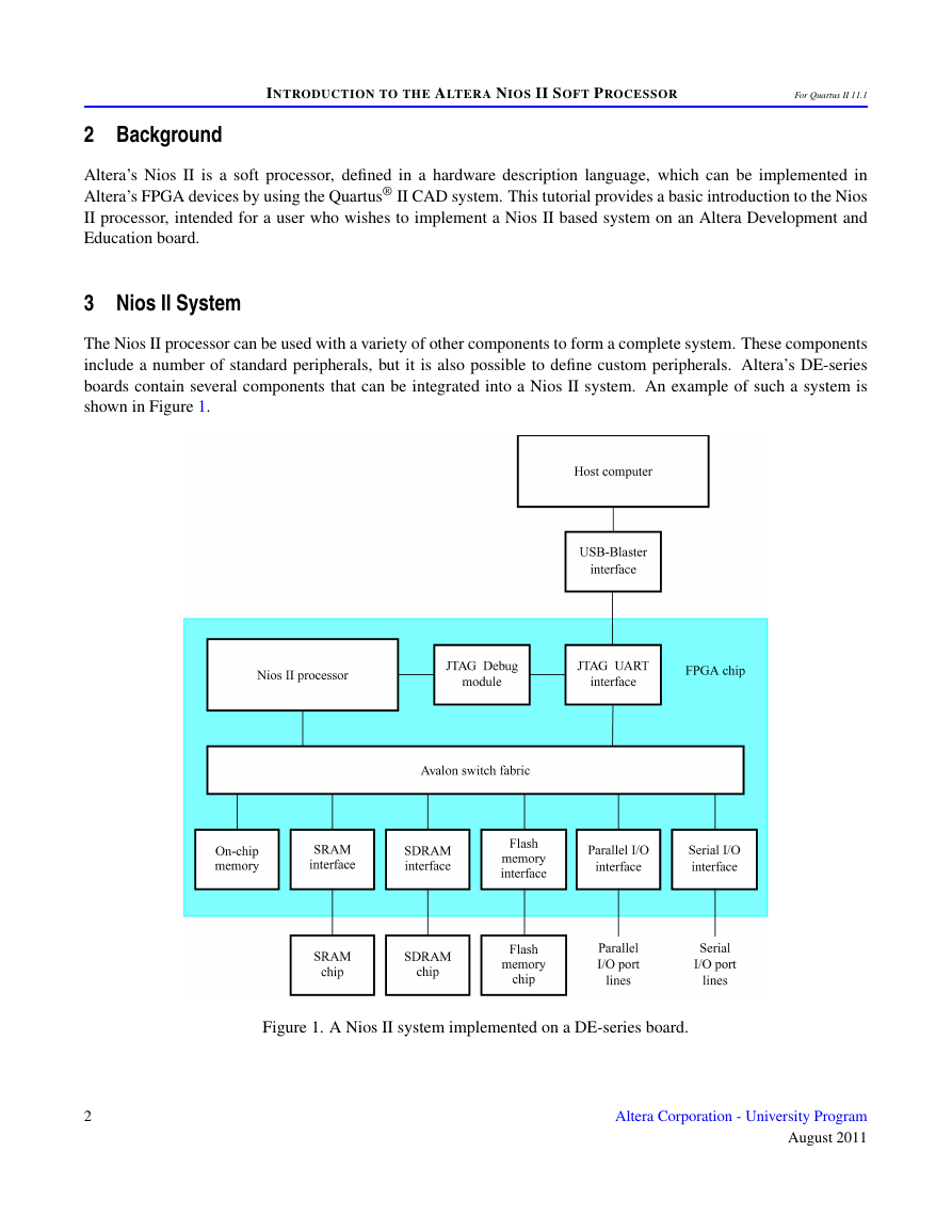
The Nios II processor can be used with a variety of other components to form a complete system. These components
include a number of standard peripherals, but it is also possible to define custom peripherals. Altera’s DE-series
boards contain several components that can be integrated into a Nios II system. An example of such a system is
shown in Figure 1.
Figure 1. A Nios II system implemented on a DE-series board.
2
Altera Corporation - University Program
August 2011
�
INTRODUCTION TO THE ALTERA NIOS II SOFT PROCESSOR
For Quartus II 11.1
The Nios II processor and the interfaces needed to connect to other chips on the board are implemented in the FPGA
chip. These components are interconnected by means of the interconnection network called the Avalon Switch
Fabric. Memory blocks in the FPGA device can be used to provide an on-chip memory for the Nios II processor.
They can be connected to the processor either directly or through the Avalon network. The SRAM and SDRAM
memory chips on the board are accessed through the appropriate interfaces. Input/output interfaces are instantiated
to provide connection to the I/O devices used in the system. A special JTAG UART interface is used to connect to
the circuitry that provides a Universal Serial Bus (USB) link to the host computer to which the DE-series board is
connected. This circuitry and the associated software is called the USB-Blaster. Another module, called the JTAG
Debug module, is provided to allow the host computer to control the Nios II processor. It makes it possible to
perform operations such as downloading programs into memory, starting and stopping execution, setting program
breakpoints, and collecting real-time execution trace data.
Since all parts of the Nios II system implemented on the FPGA chip are defined by using a hardware description
language, a knowledgeable user could write such code to implement any part of the system. This would be an
onnerous and time consuming task. Instead, one can use the SOPC Builder or Qsys tools in the Quartus II software
to implement a desired system simply by choosing the required components and specifying the parameters needed
to make each component fit the overall requirements of the system.
4 Overview of Nios II Processor Features
The Nios II processor has a number of features that can be configured by the user to meet the demands of a desired
system. The processor can be implemented in three different configurations:
• Nios II/f is a "fast" version designed for superior performance. It has the widest scope of configuration options
that can be used to optimize the processor for performance.
• Nios II/s is a "standard" version that requires less resources in an FPGA device as a trade-off for reduced
performance.
• Nios II/e is an "economy" version which requires the least amount of FPGA resources, but also has the most
limited set of user-configurable features.
The Nios II processor has a Reduced Instruction Set Computer (RISC) architecture. Its arithmetic and logic opera-
tions are performed on operands in the general purpose registers. The data is moved between the memory and these
registers by means of Load and Store instructions.
The wordlength of the Nios II processor is 32 bits. All registers are 32 bits long. Byte addresses in a 32-bit word are
assigned in little-endian style, in which the lower byte addresses are used for the less significant bytes (the rightmost
bytes) of the word. The Nios II architecture uses separate instruction and data buses, which is often referred to as
the Harvard architecture.
A Nios II processor may operate in the following modes:
• Supervisor mode – allows the processor to execute all instructions and perform all available functions. When
the processor is reset, it enters this mode.
Altera Corporation - University Program
August 2011
3
�
INTRODUCTION TO THE ALTERA NIOS II SOFT PROCESSOR
For Quartus II 11.1
• User mode – the intent of this mode is to prevent execution of some instructions that shoud be used for systems
purposes only. This mode is available only when the processor is configured to use the Memory Management
Unit (MMU) or the Memory Protection Unit (MPU).
Application programs can be run in either the User or Supervisor modes.
5 Register Structure
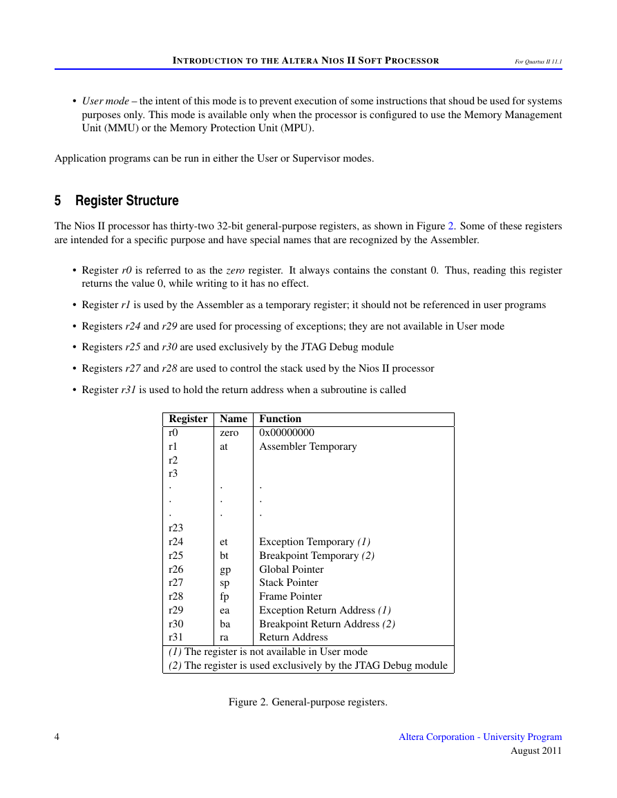
The Nios II processor has thirty-two 32-bit general-purpose registers, as shown in Figure 2. Some of these registers
are intended for a specific purpose and have special names that are recognized by the Assembler.
• Register r0 is referred to as the zero register. It always contains the constant 0. Thus, reading this register
returns the value 0, while writing to it has no effect.
• Register r1 is used by the Assembler as a temporary register; it should not be referenced in user programs
• Registers r24 and r29 are used for processing of exceptions; they are not available in User mode
• Registers r25 and r30 are used exclusively by the JTAG Debug module
• Registers r27 and r28 are used to control the stack used by the Nios II processor
• Register r31 is used to hold the return address when a subroutine is called
·
·
·
0x00000000
Assembler Temporary
Register Name Function
r0
r1
r2
r3·
·
·
r23
r24
r25
r26
r27
r28
r29
r30
r31
(1) The register is not available in User mode
(2) The register is used exclusively by the JTAG Debug module
Exception Temporary (1)
Breakpoint Temporary (2)
Global Pointer
Stack Pointer
Frame Pointer
Exception Return Address (1)
Breakpoint Return Address (2)
Return Address
zero
at
·
·
·
et
bt
gp
sp
fp
ea
ba
ra
Figure 2. General-purpose registers.
4
Altera Corporation - University Program
August 2011
�
INTRODUCTION TO THE ALTERA NIOS II SOFT PROCESSOR
For Quartus II 11.1
Nios II can have a number of 32-bit control registers. The number of registers depends on whether the MMU or the
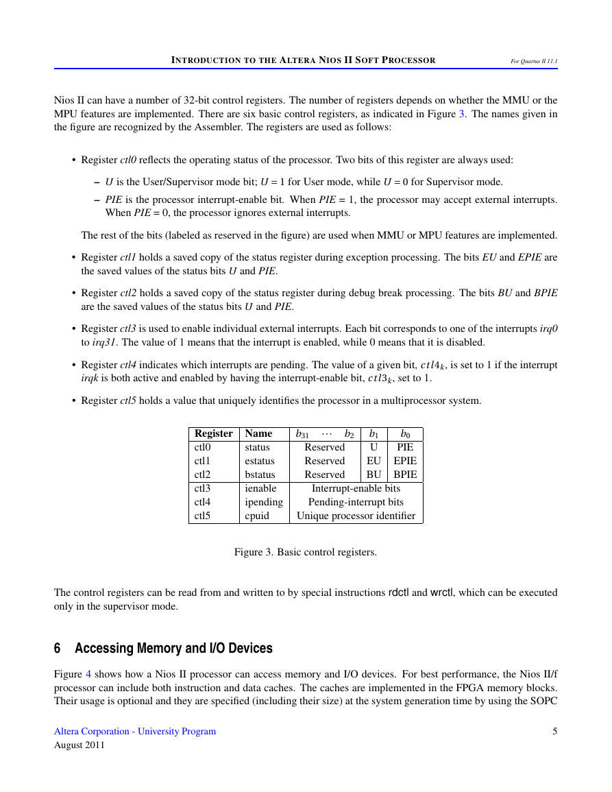
MPU features are implemented. There are six basic control registers, as indicated in Figure 3. The names given in
the figure are recognized by the Assembler. The registers are used as follows:
• Register ctl0 reflects the operating status of the processor. Two bits of this register are always used:
– U is the User/Supervisor mode bit; U = 1 for User mode, while U = 0 for Supervisor mode.
– PIE is the processor interrupt-enable bit. When PIE = 1, the processor may accept external interrupts.
When PIE = 0, the processor ignores external interrupts.
The rest of the bits (labeled as reserved in the figure) are used when MMU or MPU features are implemented.
• Register ctl1 holds a saved copy of the status register during exception processing. The bits EU and EPIE are
the saved values of the status bits U and PIE.
• Register ctl2 holds a saved copy of the status register during debug break processing. The bits BU and BPIE
are the saved values of the status bits U and PIE.
• Register ctl3 is used to enable individual external interrupts. Each bit corresponds to one of the interrupts irq0
to irq31. The value of 1 means that the interrupt is enabled, while 0 means that it is disabled.
• Register ctl4 indicates which interrupts are pending. The value of a given bit, ctl4k, is set to 1 if the interrupt
irqk is both active and enabled by having the interrupt-enable bit, ctl3k, set to 1.
• Register ctl5 holds a value that uniquely identifies the processor in a multiprocessor system.
Register Name
status
ctl0
estatus
ctl1
ctl2
bstatus
ienable
ctl3
ipending
ctl4
ctl5
cpuid
···
b2
b31
Reserved
Reserved
Reserved
b0
b1
U
PIE
EU EPIE
BU BPIE
Interrupt-enable bits
Pending-interrupt bits
Unique processor identifier
Figure 3. Basic control registers.
The control registers can be read from and written to by special instructions rdctl and wrctl, which can be executed
only in the supervisor mode.
6 Accessing Memory and I/O Devices
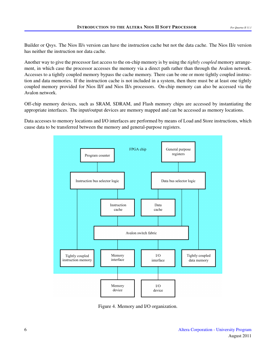
Figure 4 shows how a Nios II processor can access memory and I/O devices. For best performance, the Nios II/f
processor can include both instruction and data caches. The caches are implemented in the FPGA memory blocks.
Their usage is optional and they are specified (including their size) at the system generation time by using the SOPC
Altera Corporation - University Program
August 2011
5
�
INTRODUCTION TO THE ALTERA NIOS II SOFT PROCESSOR
For Quartus II 11.1
Builder or Qsys. The Nios II/s version can have the instruction cache but not the data cache. The Nios II/e version
has neither the instruction nor data cache.
Another way to give the processor fast access to the on-chip memory is by using the tightly coupled memory arrange-
ment, in which case the processor accesses the memory via a direct path rather than through the Avalon network.
Accesses to a tightly coupled memory bypass the cache memory. There can be one or more tightly coupled instruc-
tion and data memories. If the instruction cache is not included in a system, then there must be at least one tightly
coupled memory provided for Nios II/f and Nios II/s processors. On-chip memory can also be accessed via the
Avalon network.
Off-chip memory devices, such as SRAM, SDRAM, and Flash memory chips are accessed by instantiating the
appropriate interfaces. The input/output devices are memory mapped and can be accessed as memory locations.
Data accesses to memory locations and I/O interfaces are performed by means of Load and Store instructions, which
cause data to be transferred between the memory and general-purpose registers.
Figure 4. Memory and I/O organization.
6
Altera Corporation - University Program
August 2011
�
INTRODUCTION TO THE ALTERA NIOS II SOFT PROCESSOR
For Quartus II 11.1
7 Addressing
The Nios II processor issues 32-bit addresses. The memory space is byte-addressable. Instructions can read and
write words (32 bits), halfwords (16 bits), or bytes (8 bits) of data. Reading or writing to an address that does not
correspond to an existing memory or I/O location produces an undefined result.
There are five addressing modes provided:
• Immediate mode – a 16-bit operand is given explicitly in the instruction. This value may be sign extended to
produce a 32-bit operand in instructions that perform arithmetic operations.
• Register mode – the operand is in a processor register
• Displacement mode – the effective address of the operand is the sum of the contents of a register and a signed
16-bit displacement value given in the instruction
• Register indirect mode – the effective address of the operand is the contents of a register specified in the
instruction. This is equivalent to the displacement mode where the displacement value is equal to 0.
• Absolute mode – a 16-bit absolute address of an operand can be specified by using the displacement mode
with register r0 which always contains the value 0.
8
Instructions
All Nios II instructions are 32-bits long. In addition to machine instructions that are executed directly by the pro-
cessor, the Nios II instruction set includes a number of pseudoinstructions that can be used in assembly language
programs. The Assembler replaces each pseudoinstruction by one or more machine instructions.
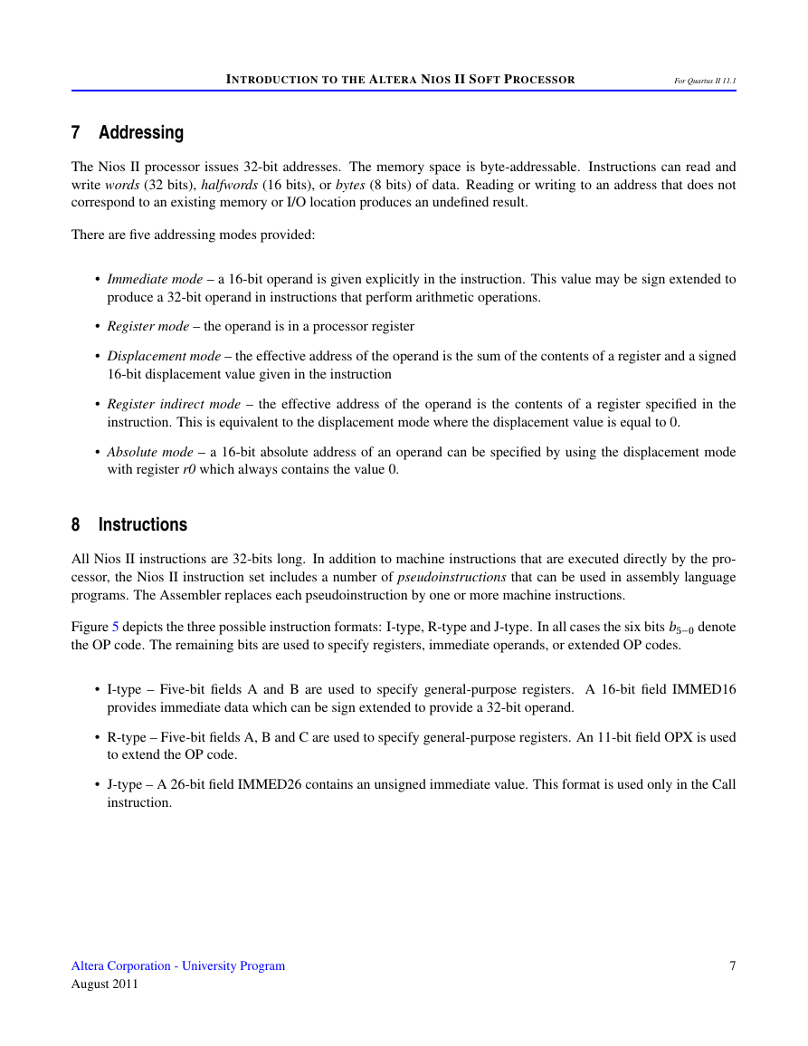
Figure 5 depicts the three possible instruction formats: I-type, R-type and J-type. In all cases the six bits b5−0 denote
the OP code. The remaining bits are used to specify registers, immediate operands, or extended OP codes.
• I-type – Five-bit fields A and B are used to specify general-purpose registers. A 16-bit field IMMED16
provides immediate data which can be sign extended to provide a 32-bit operand.
• R-type – Five-bit fields A, B and C are used to specify general-purpose registers. An 11-bit field OPX is used
to extend the OP code.
• J-type – A 26-bit field IMMED26 contains an unsigned immediate value. This format is used only in the Call
instruction.
Altera Corporation - University Program
August 2011
7
�
INTRODUCTION TO THE ALTERA NIOS II SOFT PROCESSOR
For Quartus II 11.1
Figure 5. Formats of Nios II instructions.
The following subsections discuss briefly the main features of the Nios II instruction set. For a complete description
of the instruction set, including the details of how each instruction is encoded, the reader should consult the Nios II
Processor Reference Handbook.
8.1 Load and Store Instructions
Load and Store instructions are used to move data between memory (and I/0 interfaces) and the general-purpose
registers. They are of I-type. For example, the Load Word instruction
ldw rB, byte_offset(rA)
determines the effective address of a memory location as the sum of a byte_offset value and the contents of register
A. The 16-bit byte_offset value is sign extended to 32 bits. The 32-bit memory operand is loaded into register B.
For instance, assume that the contents of register r 4 are 126010 and the byte_offset value is 8010. Then, the instruction
ldw r3, 80(r4)
loads the 32-bit operand at memory address 134010 into register r 3.
The Store Word instruction has the format
stw rB, byte_offset(rA)
8
Altera Corporation - University Program
August 2011
�


 2023年江西萍乡中考道德与法治真题及答案.doc
 2012年重庆南川中考生物真题及答案.doc
 2013年江西师范大学地理学综合及文艺理论基础考研真题.doc
 2020年四川甘孜小升初语文真题及答案I卷.doc
 2020年注册岩土工程师专业基础考试真题及答案.doc
 2023-2024学年福建省厦门市九年级上学期数学月考试题及答案.doc
 2021-2022学年辽宁省沈阳市大东区九年级上学期语文期末试题及答案.doc
 2022-2023学年北京东城区初三第一学期物理期末试卷及答案.doc
 2018上半年江西教师资格初中地理学科知识与教学能力真题及答案.doc
 2012年河北国家公务员申论考试真题及答案-省级.doc
 2020-2021学年江苏省扬州市江都区邵樊片九年级上学期数学第一次质量检测试题及答案.doc
 2022下半年黑龙江教师资格证中学综合素质真题及答案.doc