Time of Flight and LIDAR - Optical Front End Design
Anthony Vaughan
Optical Time-of-Flight (ToF) LIDAR (Light Detection
and Ranging) systems are used in a wide variety of
products including range finders, speed measurement
devices, surveying equipment, robotics, drones, 3D
mapping, and automotive advanced driver assistance
systems (ADAS). Optical ToF systems consist of a
light transmitter, usually in the form of a laser, and a
light receiver. These systems measure distance by
emitting a pulse of light onto an object and receiving
the reflected pulse of light from the object. The time it
takes for the light to travel to and from the object can
be used to calculate the distance the between the
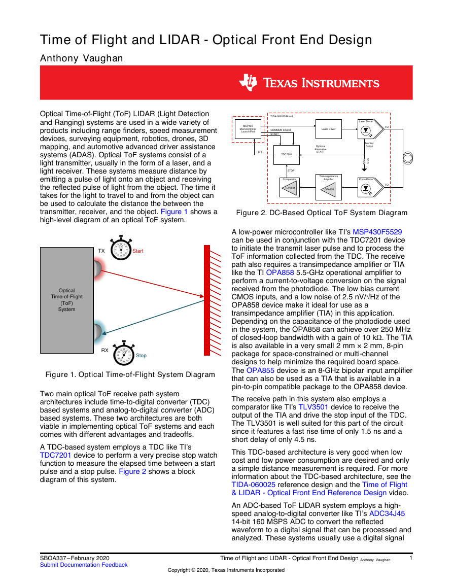
transmitter, receiver, and the object. Figure 1 shows a
high-level diagram of an optical ToF system.
Figure 1. Optical Time-of-Flight System Diagram
Two main optical ToF receive path system
architectures include time-to-digital converter (TDC)
based systems and analog-to-digital converter (ADC)
based systems. These two architectures are both
viable in implementing optical ToF systems and each
comes with different advantages and tradeoffs.
A TDC-based system employs a TDC like TI’s
TDC7201 device to perform a very precise stop watch
function to measure the elapsed time between a start
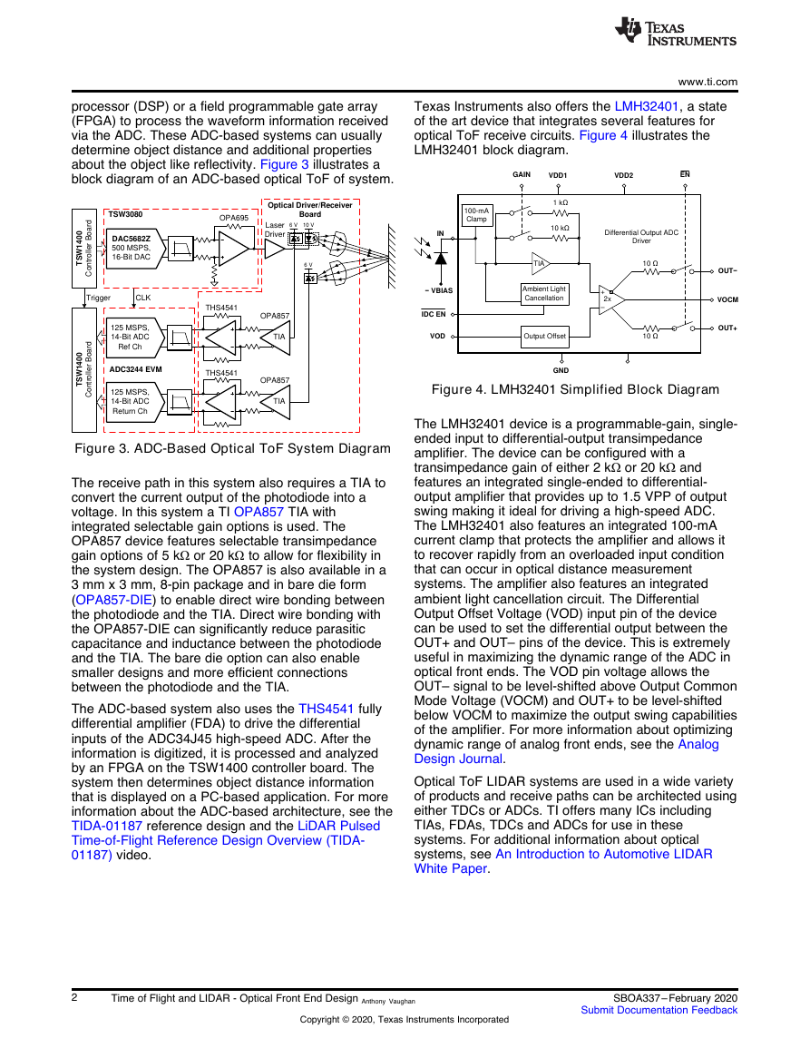
pulse and a stop pulse. Figure 2 shows a block
diagram of this system.
Figure 2. DC-Based Optical ToF System Diagram
A low-power microcontroller like TI’s MSP430F5529
can be used in conjunction with the TDC7201 device
to initiate the transmit laser pulse and to process the
ToF information collected from the TDC. The receive
path also requires a transimpedance amplifier or TIA
like the TI OPA858 5.5-GHz operational amplifier to
perform a current-to-voltage conversion on the signal
received from the photodiode. The low bias current
CMOS inputs, and a low noise of 2.5 nV/√Hz of the
OPA858 device make it ideal for use as a
transimpedance amplifier (TIA) in this application.
Depending on the capacitance of the photodiode used
in the system, the OPA858 can achieve over 250 MHz
of closed-loop bandwidth with a gain of 10 kΩ. The TIA
is also available in a very small 2 mm × 2 mm, 8-pin
package for space-constrained or multi-channel
designs to help minimize the required board space.
The OPA855 device is an 8-GHz bipolar input amplifier
that can also be used as a TIA that is available in a
pin-to-pin compatible package to the OPA858 device.
The receive path in this system also employs a
comparator like TI’s TLV3501 device to receive the
output of the TIA and drive the stop input of the TDC.
The TLV3501 is well suited for this part of the circuit
since it features a fast rise time of only 1.5 ns and a
short delay of only 4.5 ns.
This TDC-based architecture is very good when low
cost and low power consumption are desired and only
a simple distance measurement is required. For more
information about the TDC-based architecture, see the
TIDA-060025 reference design and the Time of Flight
& LIDAR - Optical Front End Reference Design video.
An ADC-based ToF LIDAR system employs a high-
speed analog-to-digital converter like TI’s ADC34J45
14-bit 160 MSPS ADC to convert the reflected
waveform to a digital signal that can be processed and
analyzed. These systems usually use a digital signal
SBOA337–February 2020
Submit Documentation Feedback
Time of Flight and LIDAR - Optical Front End Design Anthony Vaughan
1
Copyright © 2020, Texas Instruments Incorporated
TXStartRXOpticalTime-of-Flight(ToF)SystemStopMSP430MicrocontrollerLaunch PadLaser DriverTransimpedance AmplifierComparatorTDC7201Laser DiodePhoto DiodeOptional Alternative START Monitor OutputCOMMON STARTSTARTSPISTOP50 FOFOOPA858TLV3501TIDA-060025 Board�
processor (DSP) or a field programmable gate array
(FPGA) to process the waveform information received
via the ADC. These ADC-based systems can usually
determine object distance and additional properties
about the object like reflectivity. Figure 3 illustrates a
block diagram of an ADC-based optical ToF of system.
www.ti.com
Texas Instruments also offers the LMH32401, a state
of the art device that integrates several features for
optical ToF receive circuits. Figure 4 illustrates the
LMH32401 block diagram.
Figure 3. ADC-Based Optical ToF System Diagram
The receive path in this system also requires a TIA to
convert the current output of the photodiode into a
voltage. In this system a TI OPA857 TIA with
integrated selectable gain options is used. The
OPA857 device features selectable transimpedance
gain options of 5 kΩ or 20 kΩ to allow for flexibility in
the system design. The OPA857 is also available in a
3 mm x 3 mm, 8-pin package and in bare die form
(OPA857-DIE) to enable direct wire bonding between
the photodiode and the TIA. Direct wire bonding with
the OPA857-DIE can significantly reduce parasitic
capacitance and inductance between the photodiode
and the TIA. The bare die option can also enable
smaller designs and more efficient connections
between the photodiode and the TIA.
The ADC-based system also uses the THS4541 fully
differential amplifier (FDA) to drive the differential
inputs of the ADC34J45 high-speed ADC. After the
information is digitized, it is processed and analyzed
by an FPGA on the TSW1400 controller board. The
system then determines object distance information
that is displayed on a PC-based application. For more
information about the ADC-based architecture, see the
TIDA-01187 reference design and the LiDAR Pulsed
Time-of-Flight Reference Design Overview (TIDA-
01187) video.
Figure 4. LMH32401 Simplified Block Diagram
The LMH32401 device is a programmable-gain, single-
ended input to differential-output transimpedance
amplifier. The device can be configured with a
transimpedance gain of either 2 kΩ or 20 kΩ and
features an integrated single-ended to differential-
output amplifier that provides up to 1.5 VPP of output
swing making it ideal for driving a high-speed ADC.
The LMH32401 also features an integrated 100-mA
current clamp that protects the amplifier and allows it
to recover rapidly from an overloaded input condition
that can occur in optical distance measurement
systems. The amplifier also features an integrated
ambient light cancellation circuit. The Differential
Output Offset Voltage (VOD) input pin of the device
can be used to set the differential output between the
OUT+ and OUT– pins of the device. This is extremely
useful in maximizing the dynamic range of the ADC in
optical front ends. The VOD pin voltage allows the
OUT– signal to be level-shifted above Output Common
Mode Voltage (VOCM) and OUT+ to be level-shifted
below VOCM to maximize the output swing capabilities
of the amplifier. For more information about optimizing
dynamic range of analog front ends, see the Analog
Design Journal.
Optical ToF LIDAR systems are used in a wide variety
of products and receive paths can be architected using
either TDCs or ADCs. TI offers many ICs including
TIAs, FDAs, TDCs and ADCs for use in these
systems. For additional information about optical
systems, see An Introduction to Automotive LIDAR
White Paper.
2
Time of Flight and LIDAR - Optical Front End Design Anthony Vaughan
Copyright © 2020, Texas Instruments Incorporated
SBOA337–February 2020
Submit Documentation Feedback
DAC5682Z500 MSPS,16-Bit DAC6 VTHS4541OPA857LaserDriverOPA695TSW1400Controller BoardTrigger6 VTHS4541OPA857CLKADC3244 EVMTSW3080Optical Driver/ReceiverBoard10 VTIATIATSW1400Controller Board125 MSPS,14-Bit ADCRef Ch125 MSPS,14-Bit ADCReturn ChTIA1 NAmbient Light Cancellation+–100-mA ClampIDC ENVODINOUTGAINVDD1VDD2GNDENDifferential Output ADC DriverOutput OffsetVBIAS10 N10 10 OUT+ VOCM2x�
IMPORTANT NOTICE AND DISCLAIMER
TI PROVIDES TECHNICAL AND RELIABILITY DATA (INCLUDING DATASHEETS), DESIGN RESOURCES (INCLUDING REFERENCE
DESIGNS), APPLICATION OR OTHER DESIGN ADVICE, WEB TOOLS, SAFETY INFORMATION, AND OTHER RESOURCES “AS IS”
AND WITH ALL FAULTS, AND DISCLAIMS ALL WARRANTIES, EXPRESS AND IMPLIED, INCLUDING WITHOUT LIMITATION ANY
IMPLIED WARRANTIES OF MERCHANTABILITY, FITNESS FOR A PARTICULAR PURPOSE OR NON-INFRINGEMENT OF THIRD
PARTY INTELLECTUAL PROPERTY RIGHTS.
These resources are intended for skilled developers designing with TI products. You are solely responsible for (1) selecting the appropriate
TI products for your application, (2) designing, validating and testing your application, and (3) ensuring your application meets applicable
standards, and any other safety, security, or other requirements. These resources are subject to change without notice. TI grants you
permission to use these resources only for development of an application that uses the TI products described in the resource. Other
reproduction and display of these resources is prohibited. No license is granted to any other TI intellectual property right or to any third
party intellectual property right. TI disclaims responsibility for, and you will fully indemnify TI and its representatives against, any claims,
damages, costs, losses, and liabilities arising out of your use of these resources.
TI’s products are provided subject to TI’s Terms of Sale (www.ti.com/legal/termsofsale.html) or other applicable terms available either on
ti.com or provided in conjunction with such TI products. TI’s provision of these resources does not expand or otherwise alter TI’s applicable
warranties or warranty disclaimers for TI products.
Mailing Address: Texas Instruments, Post Office Box 655303, Dallas, Texas 75265
Copyright © 2020, Texas Instruments Incorporated
�


 2023年江西萍乡中考道德与法治真题及答案.doc
 2012年重庆南川中考生物真题及答案.doc
 2013年江西师范大学地理学综合及文艺理论基础考研真题.doc
 2020年四川甘孜小升初语文真题及答案I卷.doc
 2020年注册岩土工程师专业基础考试真题及答案.doc
 2023-2024学年福建省厦门市九年级上学期数学月考试题及答案.doc
 2021-2022学年辽宁省沈阳市大东区九年级上学期语文期末试题及答案.doc
 2022-2023学年北京东城区初三第一学期物理期末试卷及答案.doc
 2018上半年江西教师资格初中地理学科知识与教学能力真题及答案.doc
 2012年河北国家公务员申论考试真题及答案-省级.doc
 2020-2021学年江苏省扬州市江都区邵樊片九年级上学期数学第一次质量检测试题及答案.doc
 2022下半年黑龙江教师资格证中学综合素质真题及答案.doc