S3C44B0X RISC MICROPROCESSOR
PRODUCT OVERVIEW
1 PRODUCT OVERVIEW
INTRODUCTION
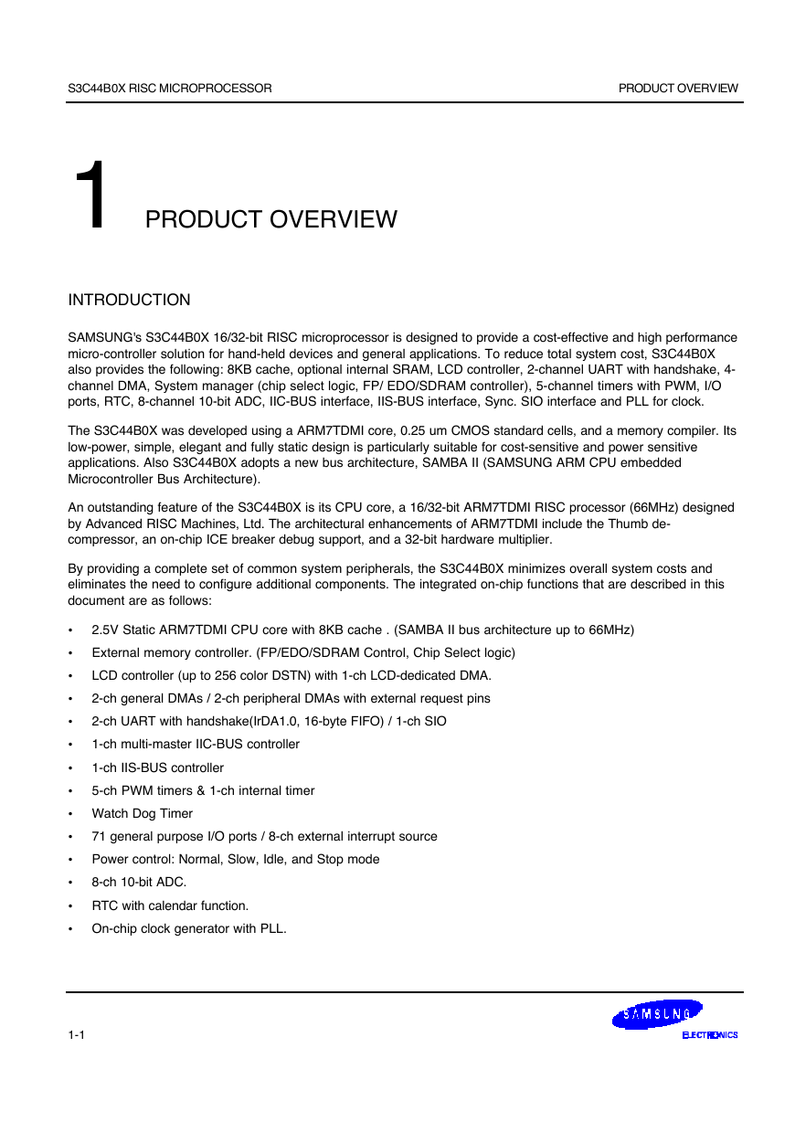
SAMSUNG's S3C44B0X 16/32-bit RISC microprocessor is designed to provide a cost-effective and high performance
micro-controller solution for hand-held devices and general applications. To reduce total system cost, S3C44B0X
also provides the following: 8KB cache, optional internal SRAM, LCD controller, 2-channel UART with handshake, 4-
channel DMA, System manager (chip select logic, FP/ EDO/SDRAM controller), 5-channel timers with PWM, I/O
ports, RTC, 8-channel 10-bit ADC, IIC-BUS interface, IIS-BUS interface, Sync. SIO interface and PLL for clock.
The S3C44B0X was developed using a ARM7TDMI core, 0.25 um CMOS standard cells, and a memory compiler. Its
low-power, simple, elegant and fully static design is particularly suitable for cost-sensitive and power sensitive
applications. Also S3C44B0X adopts a new bus architecture, SAMBA II (SAMSUNG ARM CPU embedded
Microcontroller Bus Architecture).
An outstanding feature of the S3C44B0X is its CPU core, a 16/32-bit ARM7TDMI RISC processor (66MHz) designed
by Advanced RISC Machines, Ltd. The architectural enhancements of ARM7TDMI include the Thumb de-
compressor, an on-chip ICE breaker debug support, and a 32-bit hardware multiplier.
By providing a complete set of common system peripherals, the S3C44B0X minimizes overall system costs and
eliminates the need to configure additional components. The integrated on-chip functions that are described in this
document are as follows:
2.5V Static ARM7TDMI CPU core with 8KB cache . (SAMBA II bus architecture up to 66MHz)
External memory controller. (FP/EDO/SDRAM Control, Chip Select logic)
LCD controller (up to 256 color DSTN) with 1-ch LCD-dedicated DMA.
2-ch general DMAs / 2-ch peripheral DMAs with external request pins
2-ch UART with handshake(IrDA1.0, 16-byte FIFO) / 1-ch SIO
1-ch multi-master IIC-BUS controller
1-ch IIS-BUS controller
5-ch PWM timers & 1-ch internal timer
•
•
•
•
•
•
•
•
•
1-1
•
• Watch Dog Timer
•
71 general purpose I/O ports / 8-ch external interrupt source
Power control: Normal, Slow, Idle, and Stop mode
8-ch 10-bit ADC.
RTC with calendar function.
•
• On-chip clock generator with PLL.
�
PRODUCT OVERVIEW
S3C44B0X RISC MICROPROCESSOR
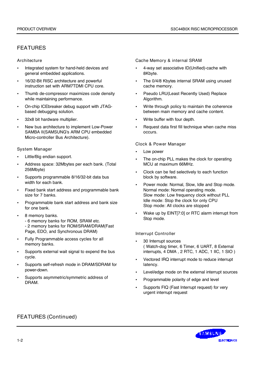
FEATURES
Cache Memory & internal SRAM
•
4-way set associative ID(Unified)-cache with
8Kbyte.
The 0/4/8 Kbytes internal SRAM using unused
cache memory.
Pseudo LRU(Least Recently Used) Replace
Algorithm.
• Write through policy to maintain the coherence
between main memory and cache content.
• Write buffer with four depth.
•
Request data first fill technique when cache miss
occurs.
Clock & Power Manager
•
Low power
The on-chip PLL makes the clock for operating
MCU at maximum 66MHz.
Clock can be fed selectively to each function
block by software.
Power mode: Normal, Slow, Idle and Stop mode.
Normal mode: Normal operating mode.
Slow mode: Low frequency clock without PLL
Idle mode: Stop the clock for only CPU
Stop mode: All clocks are stopped
• Wake up by EINT[7:0] or RTC alarm interrupt from
Stop mode.
Interrupt Controller
•
30 Interrupt sources
( Watch-dog timer, 6 Timer, 6 UART, 8 External
interrupts, 4 DMA , 2 RTC, 1 ADC, 1 IIC, 1 SIO )
Vectored IRQ interrupt mode to reduce interrupt
latency.
Level/edge mode on the external interrupt sources
Programmable polarity of edge and level
Supports FIQ (Fast Interrupt request) for very
urgent interrupt request
•
•
•
•
•
•
•
•
•
Architecture
•
Integrated system for hand-held devices and
general embedded applications.
16/32-Bit RISC architecture and powerful
instruction set with ARM7TDMI CPU core.
Thumb de-compressor maximizes code density
while maintaining performance.
• On-chip ICEbreaker debug support with JTAG-
based debugging solution.
32x8 bit hardware multiplier.
New bus architecture to implement Low-Power
SAMBA II(SAMSUNG's ARM CPU embedded
Micro-controller Bus Architecture).
System Manager
•
Little/Big endian support.
Address space: 32Mbytes per each bank. (Total
256Mbyte)
Supports programmable 8/16/32-bit data bus
width for each bank.
Fixed bank start address and programmable bank
size for 7 banks.
Programmable bank start address and bank size
for one bank.
8 memory banks.
- 6 memory banks for ROM, SRAM etc.
- 2 memory banks for ROM/SRAM/DRAM(Fast
Page, EDO, and Synchronous DRAM)
Fully Programmable access cycles for all
memory banks.
Supports external wait signal to expend the bus
cycle.
Supports self-refresh mode in DRAM/SDRAM for
power-down.
Supports asymmetric/symmetric address of
DRAM.
•
•
•
•
•
•
•
•
•
•
•
•
•
FEATURES (Continued)
1-2
�
•
•
•
•
•
•
•
•
•
General purpose input/output ports
•
•
8 external interrupt ports
71 multiplexed input/output ports
A/D Converter
•
8-ch multiplexed ADC.
• Max. 100KSPS/10-bit.
UART
•
•
transmit/receive
•
2-channel UART with DMA-based or interrupt-
based operation
Supports 5-bit, 6-bit, 7-bit, or 8-bit serial data
transmit/receive
Supports H/W handshaking during
Programmable baud rate
Supports IrDA 1.0 (115.2kbps)
Loop back mode for testing
Each channel have two internal 32-byte FIFO for
Rx and Tx.
LCD Controller
•
Supports color/monochrome/gray LCD panel
Supports single scan and dual scan displays
Supports virtual screen function
System memory is used as display memory
Dedicated DMA for fetching image data from
system memory
Programmable screen size
•
• Gray level: 16 gray levels
•
256 Color levels
S3C44B0X RISC MICROPROCESSOR
PRODUCT OVERVIEW
Timer with PWM (Pulse Width Modulation)
•
5-ch 16-bit Timer with PWM / 1-ch 16-bit internal
timer with DMA-based or interrupt-based
operation
Programmable duty cycle, frequency, and polarity
Dead-zone generation.
Supports external clock source.
•
•
•
RTC (Real Time Clock)
•
Full clock feature: msec, sec, min, hour, day,
week, month, year.
32.768 KHz operation.
Alarm interrupt for CPU wake-up.
Time tick interrupt
DMA Controller
•
2 channel general purpose Direct Memory Access
controller without CPU intervention.
2 channel Bridge DMA (peripheral DMA)
controller.
Support IO to memory, memory to IO, IO to IO
with the Bridge DMA which has 6 type's DMA
requestor: Software, 4 internal function blocks
(UART, SIO, Timer, IIS), and External pins.
Programmable priority order between DMAs (fixed
or round-robin mode)
Burst transfer mode to enhance the transfer rate
on the FPDRAM, EDODRAM and SDRAM.
Supports fly-by mode on the memory to external
device and external device to memory transfer
mode
•
•
•
•
•
•
•
1-3
�
PRODUCT OVERVIEW
S3C44B0X RISC MICROPROCESSOR
FEATURES (Continued)
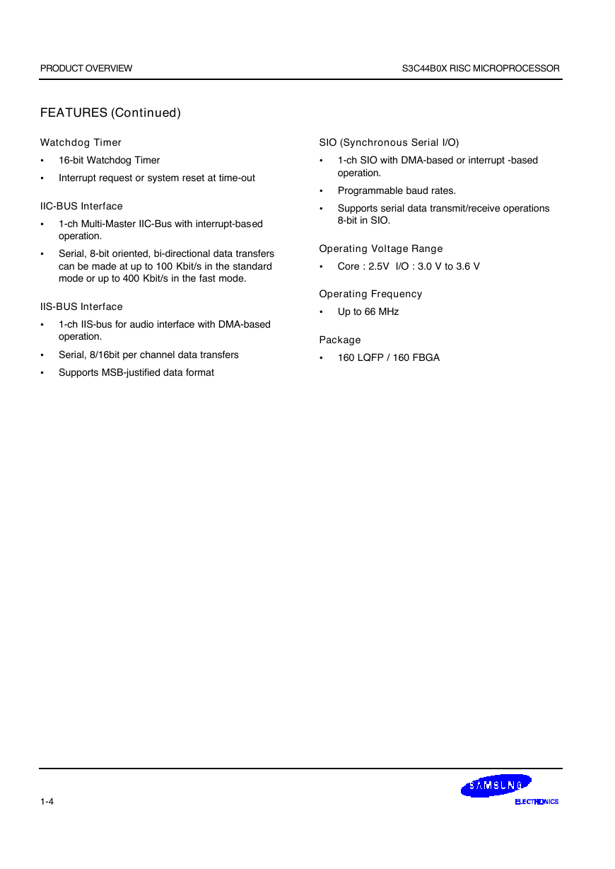
Watchdog Timer
•
16-bit Watchdog Timer
Interrupt request or system reset at time-out
SIO (Synchronous Serial I/O)
•
1-ch SIO with DMA-based or interrupt -based
operation.
Programmable baud rates.
Supports serial data transmit/receive operations
8-bit in SIO.
•
•
Operating Voltage Range
•
Core : 2.5V I/O : 3.0 V to 3.6 V
Operating Frequency
•
Up to 66 MHz
Package
•
160 LQFP / 160 FBGA
IIC-BUS Interface
•
1-ch Multi-Master IIC-Bus with interrupt-based
operation.
Serial, 8-bit oriented, bi-directional data transfers
can be made at up to 100 Kbit/s in the standard
mode or up to 400 Kbit/s in the fast mode.
IIS-BUS Interface
•
1-ch IIS-bus for audio interface with DMA-based
operation.
Serial, 8/16bit per channel data transfers
Supports MSB-justified data format
•
•
•
•
1-4
�
S3C44B0X RISC MICROPROCESSOR
PRODUCT OVERVIEW
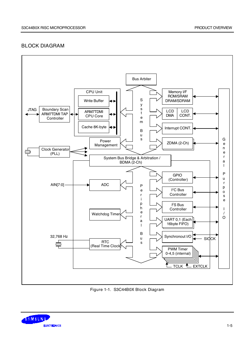
BLOCK DIAGRAM
Bus Arbiter
S
y
s
t
e
m
B
u
s
CPU Unit
Write Buffer
ARM7TDMI
CPU Core
Cache 8K-byte
Power
Management
System Bus Bridge & Arbitration /
BDMA (2-Ch)
JTAG
Boundary Scan
ARM7TDMI TAP
Controller
Clock Generator
(PLL)
AIN[7:0]
ADC
Watchdog Timer
32,768 Hz
RTC
(Real Time Clock)
P
e
r
i
p
h
e
r
a
l
B
u
s
Memory I/F
ROM/SRAM
DRAM/SDRAM
LCD
DMA
LCD
CONT.
Interrupt CONT.
ZDMA (2-Ch)
GPIO
(Controller)
I2C Bus
Controller
I2S Bus
Controller
UART 0,1 (Each
16byte FIFO)
Synchronout I/O
SIOCK
PWM Timer
0-4,5 (internal)
TCLK
EXTCLK
Figure 1-1. S3C44B0X Block Diagram
G
e
n
e
r
a
l
P
u
r
p
o
s
e
I
/
O
1-5
�
PRODUCT OVERVIEW
S3C44B0X RISC MICROPROCESSOR
PIN ASSIGNMENTS
D
A
T
A
1
6
/
I
I
S
L
R
C
K
G
P
C
0
/
D
A
T
A
1
4
D
A
T
A
1
5
D
A
T
A
1
7
/
I
I
/
S
D
O
G
P
C
1
D
A
T
A
1
8
/
I
I
S
D
I
/
G
P
C
2
D
A
T
A
1
9
/
I
I
/
S
C
L
K
G
P
C
3
/
/
/
D
A
T
A
2
0
V
D
7
G
P
C
4
D
A
T
A
2
1
V
D
6
G
P
C
5
D
A
T
A
2
2
V
D
5
G
P
C
6
/
/
/
1
2
0
1
1
9
1
1
8
1
1
7
1
1
6
1
1
5
1
1
4
1
1
3
1
1
2
/
/
D
A
T
A
2
4
n
X
D
A
C
K
1
G
P
C
8
D
A
T
A
2
5
n
X
D
R
E
Q
1
G
P
C
9
/
/
V
D
D
/
/
D
A
T
A
2
6
n
R
T
S
1
G
P
C
1
0
D
A
T
A
2
7
n
C
T
S
1
G
P
C
1
1
/
/
/
D
A
T
A
2
8
T
x
D
1
G
P
C
1
2
/
/
/
D
A
T
A
3
0
n
R
T
S
0
G
P
C
1
4
D
A
T
A
3
1
n
C
T
S
0
G
P
C
1
5
/
/
/
D
A
T
A
2
9
R
x
D
1
G
P
C
1
3
/
1
0
9
1
0
8
1
0
7
1
0
6
1
0
5
1
0
4
1
0
3
1
0
2
1
0
1
/
D
A
T
A
2
3
V
D
4
G
P
C
7
/
V
S
S
1
1
1
1
1
0
/
R
x
D
0
G
P
E
2
/
T
x
D
0
G
P
E
1
/
V
D
0
G
P
D
0
/
/
/
V
D
1
G
P
D
1
V
D
2
G
P
D
2
V
D
3
G
P
D
3
/
V
C
L
K
G
P
D
4
I
V
L
N
E
G
P
D
5
/
/
V
M
G
P
D
6
V
F
R
A
M
E
G
P
D
7
/
V
S
S
O
I
V
D
D
R
T
C
E
X
T
A
L
1
X
T
A
L
1
V
D
D
A
D
C
9
9
9
8
1
0
0
9
7
9
6
9
5
9
4
9
3
9
2
9
1
9
0
8
9
8
8
8
7
8
6
A
V
C
O
M
A
R
E
F
B
8
5
8
4
3
6
3
7
/
/
E
x
I
N
T
2
n
C
T
S
0
G
P
G
2
E
x
I
N
T
3
n
R
T
S
0
G
P
G
3
/
/
A
R
E
F
T
I
A
N
7
I
A
N
6
8
3
8
2
8
1
80
79
78
77
76
75
74
73
72
71
70
69
68
67
66
65
64
63
62
61
60
59
58
57
56
55
54
53
52
51
50
49
48
47
46
45
44
43
42
41
AIN5
AIN4
AIN3
AIN2
AIN1
AIN0
VSSADC
VSSIO
TOUT4/VD7/GPE7
TOUT3/VD6/GPE6
TOUT2/TCLK/GPE5
TOUT1/TCLK/GPE4
TOUT0/GPE3
EXTCLK
PLLCAP
EXTAL0
XTAL0
VSS
VDD
IICSCL/GPF0
IICSDA/GPF1
SIOTxD/nRTS1/IISLRCK/GPF5
SIORDY/TxD1/IISDO/GPF6
SIORxD/RxD1/IISDI/GPF7
SIOCLK/nCTS1/IISCLK/GPF8
ENDIAN/CODECLK/GPE8
OM3
OM2
OM1
OM0
nRESET
CLKout/GPE0
VSSIO
VDDIO
TDO
TDI
TMS
TCK
nTRST
ExINT7/IISLRCK/GPG7
3
8
3
9
4
0
E
x
I
N
T
4
E
x
I
N
T
5
E
x
I
N
T
6
/
I
I
/
S
C
L
K
G
P
G
4
/
I
I
/
I
I
S
D
I
/
G
P
G
5
/
S
D
O
G
P
G
6
S3C44B0X
160-QFP
1
8
1
9
2
0
n
G
C
S
1
G
P
B
6
n
G
C
S
2
G
P
B
7
n
G
C
S
3
G
P
B
8
/
/
/
2
1
2
2
2
3
2
4
2
5
2
6
2
7
2
8
2
9
3
0
3
1
3
2
3
3
3
4
3
5
V
D
D
V
S
S
n
G
C
S
4
G
P
B
9
/
S
C
K
E
G
P
B
0
S
C
L
K
G
P
B
1
/
/
I
n
W
A
T
G
P
F
2
/
n
G
C
S
5
G
P
B
1
0
/
:
:
n
G
C
S
6
n
S
C
S
0
n
R
A
S
0
n
G
C
S
7
n
S
C
S
1
n
R
A
S
1
:
:
/
E
x
I
N
T
0
V
D
4
G
P
G
0
/
/
/
n
X
D
R
E
Q
0
n
X
B
R
E
Q
G
P
F
4
n
X
D
A
C
K
0
n
X
B
A
C
K
G
P
F
3
/
/
V
D
D
V
S
S
/
E
x
I
N
T
1
V
D
5
G
P
G
1
/
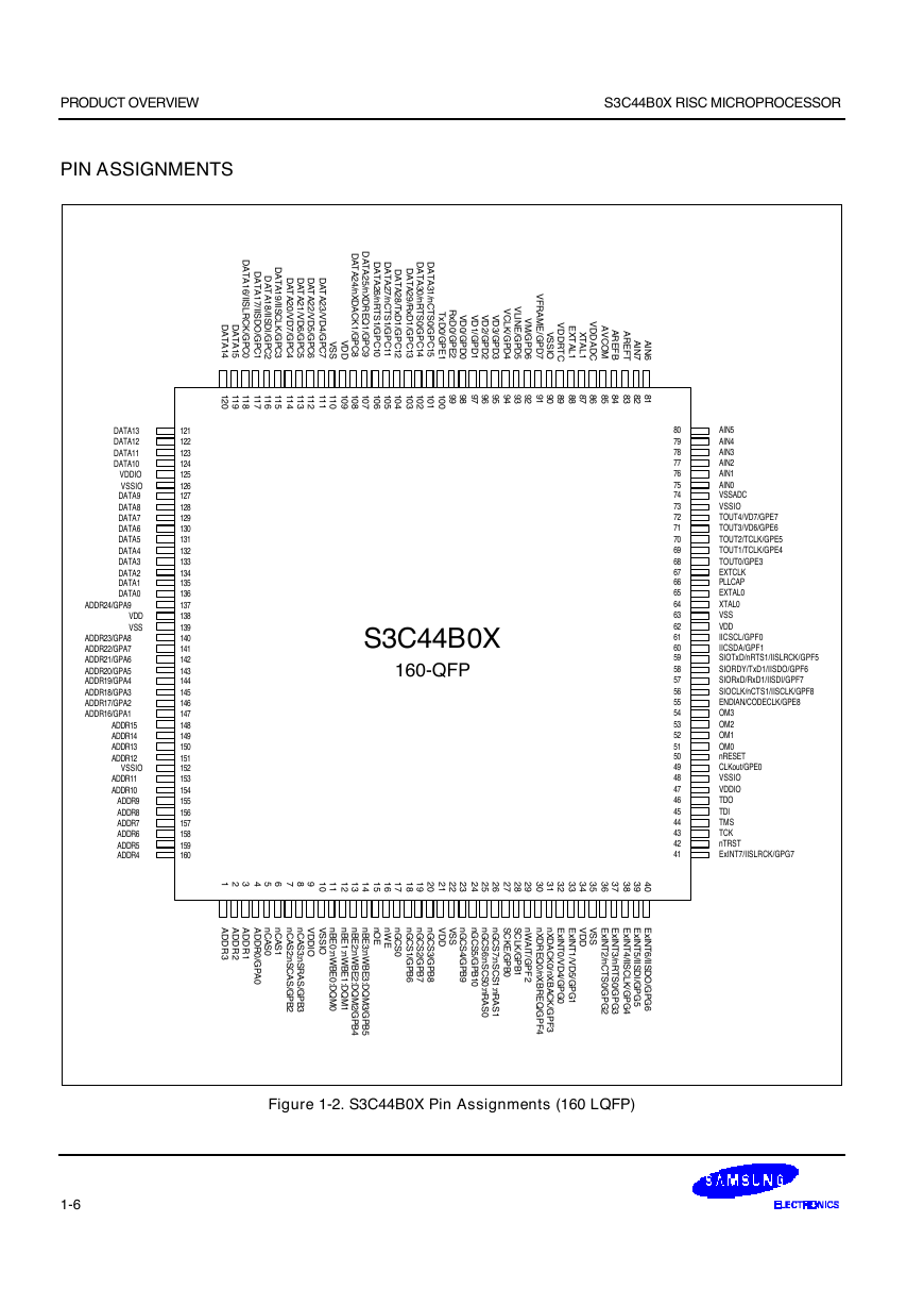
Figure 1-2. S3C44B0X Pin Assignments (160 LQFP)
121
122
123
124
125
126
127
128
129
130
131
132
133
134
135
136
137
138
139
140
141
142
143
144
145
146
147
148
149
150
151
152
153
154
155
156
157
158
159
160
1234567891
0
1
1
1
2
1
3
1
4
1
5
1
6
1
7
n
O
E
n
W
E
n
G
C
S
0
A
D
D
R
3
A
D
D
R
2
A
D
D
R
1
n
C
A
S
0
n
C
A
S
1
A
D
D
R
0
G
P
A
0
/
V
D
D
O
I
:
:
n
C
A
S
2
n
S
C
A
S
G
P
B
2
n
C
A
S
3
n
S
R
A
S
G
P
B
3
/
/
V
S
S
O
I
:
n
B
E
0
n
W
B
E
0
D
Q
M
0
:
:
n
B
E
1
n
W
B
E
1
D
Q
M
1
:
:
:
n
B
E
2
n
W
B
E
2
D
Q
M
2
G
P
B
4
n
B
E
3
n
W
B
E
3
D
Q
M
3
G
P
B
5
:
/
:
/
DATA13
DATA12
DATA11
DATA10
VDDIO
VSSIO
DATA9
DATA8
DATA7
DATA6
DATA5
DATA4
DATA3
DATA2
DATA1
DATA0
VDD
VSS
ADDR24/GPA9
ADDR23/GPA8
ADDR22/GPA7
ADDR21/GPA6
ADDR20/GPA5
ADDR19/GPA4
ADDR18/GPA3
ADDR17/GPA2
ADDR16/GPA1
ADDR15
ADDR14
ADDR13
ADDR12
VSSIO
ADDR11
ADDR10
ADDR9
ADDR8
ADDR7
ADDR6
ADDR5
ADDR4
1-6
�
S3C44B0X RISC MICROPROCESSOR
PRODUCT OVERVIEW
P
N
M
L
K
J
H
G
F
E
D
C
B
A
Ball Pad A1
Corner Indicator
1
2
3
4
5
6
7
8
9
10
11
12
13
14
Bottom View
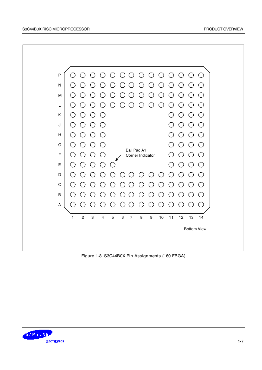
Figure 1-3. S3C44B0X Pin Assignments (160 FBGA)
1-7
�
PRODUCT OVERVIEW
S3C44B0X RISC MICROPROCESSOR
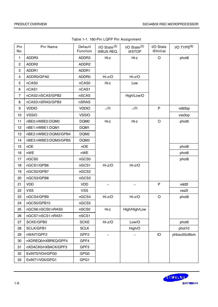
Table 1-1. 160-Pin LQFP Pin Assignment
Pin
No.
Pin Name
Default
Function
I/O State(2)
@BUS REQ.
I/O State(2)
@STOP
I/O State
@Initial
I/O TYPE(6)
Hi-z
Hi-z
O
phot8
Hi-z/O
Hi-z
Hi-z/O
Low
High/Low/O
–(3)
Hi-z
–(3)
Hi-z
Hi-z/O
Hi-z/O
Hi-z/O
Hi-z/O
Hi-z
High/High/Low
Hi-z/O
Low/O
High/O
P
O
P
O
vdd3op
vss3op
phot6
phot8
phot6
phot8
vdd2I
vss2I
phot8
phot6
phot10
IO
phbsu50ct8sm
ADDR3
ADDR2
ADDR1
ADDR0/GPA0
nCAS0
nCAS1
nCAS2:nSCAS/GPB2
nCAS3:nSRAS/GPB3
VDDIO
VSSIO
nBE0:nWBE0:DQM0
nBE1:nWBE1:DQM1
nBE2:nWBE2:DQM2/GPB4
nBE3:nWBE3:DQM3/GPB5
nOE
nWE
nGCS0
nGCS1/GPB6
nGCS2/GPB7
nGCS3/GPB8
VDD
VSS
nGCS4/GPB9
nGCS5/GPB10
nGCS6:nSCS0:nRAS0
nGCS7:nSCS1:nRAS1
SCKE/GPB0
SCLK/GPB1
nWAIT/GPF2
nXDREQ0/nXBREQ/GPF4
nXDACK0/nXBACK/GPF3
ExINT0/VD4/GPG0
ExINT1/VD5/GPG1
ADDR3
ADDR2
ADDR1
ADDR0
nCAS0
nCAS1
nSCAS
nSRAS
VDDIO
VSSIO
DQM0
DQM1
DQM2
DQM3
nOE
nWE
nGCS0
nGCS1
nGCS2
nGCS3
VDD
VSS
nGCS4
nGCS5
nSCS0
nSCS1
SCKE
SCLK
GPF2
GPF4
GPF3
GPG0
GPG1
1
2
3
4
5
6
7
8
9
10
11
12
13
14
15
16
17
18
19
20
21
22
23
24
25
26
27
28
29
30
31
32
33
1-8
-
-
-
-
�



 2023年江西萍乡中考道德与法治真题及答案.doc
 2012年重庆南川中考生物真题及答案.doc
 2013年江西师范大学地理学综合及文艺理论基础考研真题.doc
 2020年四川甘孜小升初语文真题及答案I卷.doc
 2020年注册岩土工程师专业基础考试真题及答案.doc
 2023-2024学年福建省厦门市九年级上学期数学月考试题及答案.doc
 2021-2022学年辽宁省沈阳市大东区九年级上学期语文期末试题及答案.doc
 2022-2023学年北京东城区初三第一学期物理期末试卷及答案.doc
 2018上半年江西教师资格初中地理学科知识与教学能力真题及答案.doc
 2012年河北国家公务员申论考试真题及答案-省级.doc
 2020-2021学年江苏省扬州市江都区邵樊片九年级上学期数学第一次质量检测试题及答案.doc
 2022下半年黑龙江教师资格证中学综合素质真题及答案.doc