Title Page
Acknowledgements
Table of Contents
List of Figures
List of Tables
About This Book
The MindShare Technology Series
Cautionary Note
Intended Audience
Prerequisite Knowledge
Book Topics and Organization
Documentation Conventions
PCI Express™
Hexadecimal Notation
Binary Notation
Decimal Notation
Bits, Bytes and Transfers Notation
Bit Fields
Active Signal States
Visit Our Web Site
We Want Your Feedback
Part One: The Big Picture
Chapter 1: Background
Introduction
PCI and PCI-X
PCI Basics
Basics of a PCI-Based System
PCI Bus Initiator and Target
Typical PCI Bus Cycle
Reflected-Wave Signaling
PCI Bus Architecture Perspective
PCI Transaction Models
Programmed I/O
Direct Memory Access (DMA)
Peer-to-Peer
PCI Bus Arbitration
PCI Inefficiencies
PCI Retry Protocol
PCI Disconnect Protocol
PCI Interrupt Handling
PCI Error Handling
PCI Address Space Map
PCI Configuration Cycle Generation
PCI Function Configuration Register Space
Higher-bandwidth PCI
Limitations of 66 MHz PCI bus
Signal Timing Problems with the Parallel PCI Bus Model beyond 66 MHz
Introducing PCI-X
PCI-X System Example
PCI-X Transactions
PCI-X Features
Split-Transaction Model
Message Signaled Interrupts
Transaction Attributes
No Snoop (NS):
Relaxed Ordering (RO):
Higher Bandwidth PCI-X
Problems with the Common Clock Approach of PCI and PCI-X 1.0 Parallel Bus Model
PCI-X 2.0 Source-Synchronous Model
Chapter 2: PCIe Architecture Overview
Introduction to PCI Express
Software Backward Compatibility
Serial Transport
The Need for Speed
Overcoming Problems
Bandwidth
PCIe Bandwidth Calculation
Differential Signals
No Common Clock
Packet-based Protocol
Links and Lanes
Scalable Performance
Flexible Topology Options
Some Definitions
Root Complex
Switches and Bridges
Native PCIe Endpoints and Legacy PCIe Endpoints
Software Compatibility Characteristics
System Examples
Introduction to Device Layers
Device Core / Software Layer
Transaction Layer
TLP (Transaction Layer Packet) Basics
TLP Packet Assembly
TLP Packet Disassembly
Non-Posted Transactions
Ordinary Reads
Locked Reads
IO and Configuration Writes
Posted Writes
Memory Writes
Message Writes
Transaction Ordering
Data Link Layer
DLLPs (Data Link Layer Packets)
DLLP Assembly
DLLP Disassembly
Ack/Nak Protocol
Flow Control
Power Management
Physical Layer
General
Physical Layer - Logical
Link Training and Initialization
Physical Layer - Electrical
Ordered Sets
Protocol Review Example
Memory Read Request
Completion with Data
Chapter 3: Configuration Overview
Definition of Bus, Device and Function
PCIe Buses
PCIe Devices
PCIe Functions
Configuration Address Space
PCI-Compatible Space
Extended Configuration Space
Host-to-PCI Bridge Configuration Registers
General
Only the Root Sends Configuration Requests
Generating Configuration Transactions
Legacy PCI Mechanism
Configuration Address Port
Bus Compare and Data Port Usage
Single Host System
Multi-Host System
Enhanced Configuration Access Mechanism
General
Some Rules
Configuration Requests
Type 0 Configuration Request
Type 1 Configuration Request
Example PCI-Compatible Configuration Access
Example Enhanced Configuration Access
Enumeration - Discovering the Topology
Discovering the Presence or Absence of a Function
Device not Present
Device not Ready
Determining if a Function is an Endpoint or Bridge
Single Root Enumeration Example
Multi-Root Enumeration Example
General
Multi-Root Enumeration Process
Hot-Plug Considerations
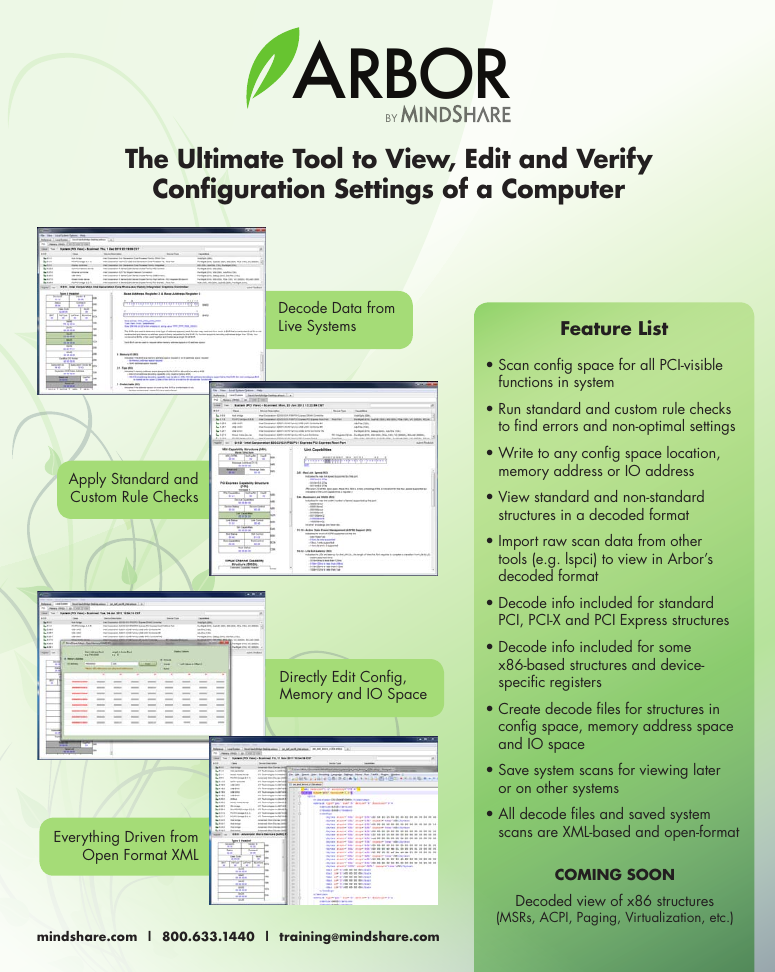
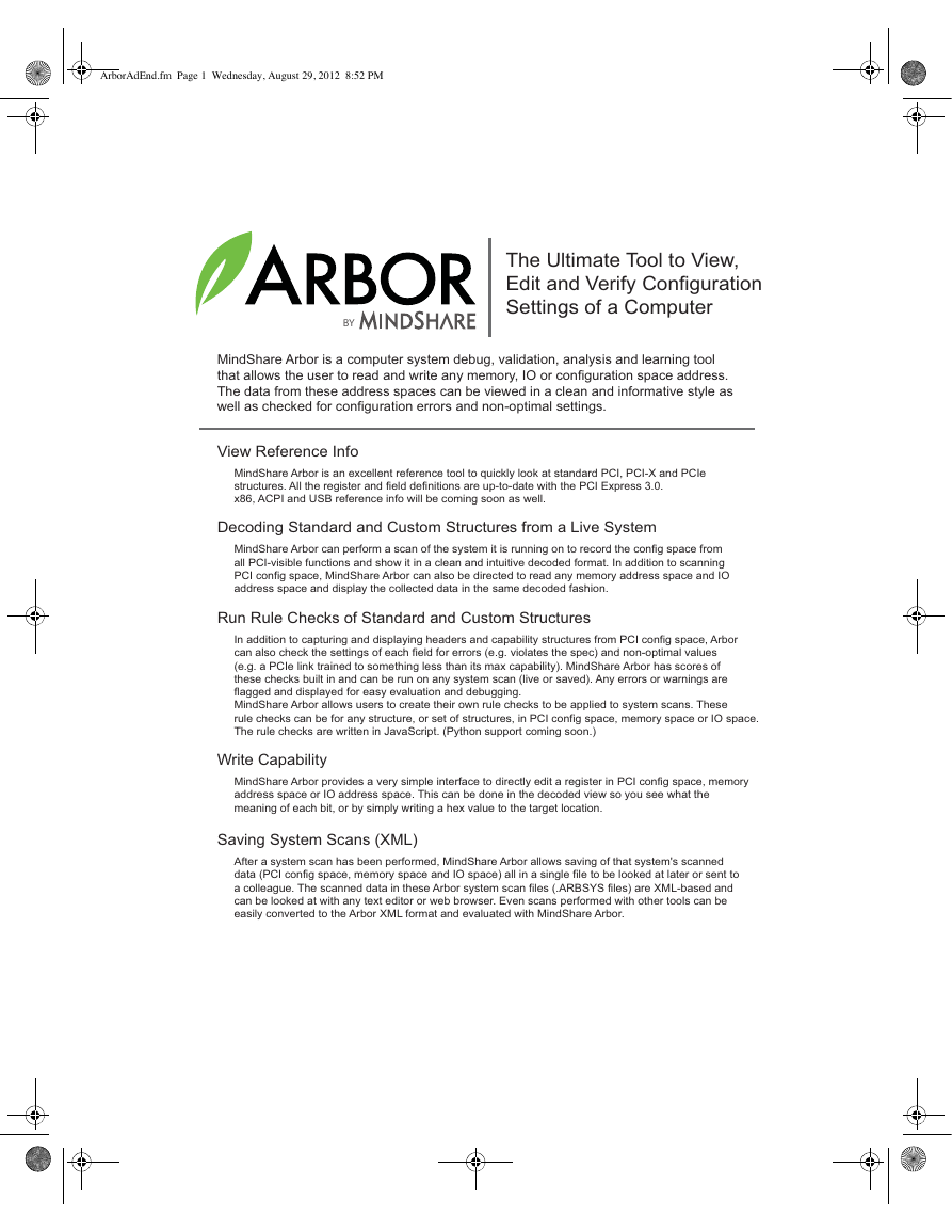
MindShare Arbor: Debug/Validation/Analysis and Learning Software Tool
General
MindShare Arbor Feature List
Chapter 4: Address Space & Transaction Routing
I Need An Address
Configuration Space
Memory and IO Address Spaces
General
Prefetchable vs. Non-prefetchable Memory Space
Base Address Registers (BARs)
General
BAR Example 1: 32-bit Memory Address Space Request
BAR Example 2: 64-bit Memory Address Space Request
BAR Example 3: IO Address Space Request
All BARs Must Be Evaluated Sequentially
Resizable BARs
Base and Limit Registers
General
Prefetchable Range (P-MMIO)
Non-Prefetchable Range (NP-MMIO)
IO Range
Unused Base and Limit Registers
Sanity Check: Registers Used For Address Routing
TLP Routing Basics
Receivers Check For Three Types of Traffic
Routing Elements
Three Methods of TLP Routing
General
Purpose of Implicit Routing and Messages
Why Messages?
How Implicit Routing Helps
Split Transaction Protocol
Posted versus Non-Posted
Header Fields Define Packet Format and Type
General
Header Format/Type Field Encodings
TLP Header Overview
Applying Routing Mechanisms
ID Routing
Bus Number, Device Number, Function Number Limits
Key TLP Header Fields in ID Routing
Endpoints: One Check
Switches (Bridges): Two Checks Per Port
Address Routing
Key TLP Header Fields in Address Routing
TLPs with 32-Bit Address
TLPs with 64-Bit Address
Endpoint Address Checking
Switch Routing
Downstream Traveling TLPs (Received on Primary Interface)
Upstream Traveling TLPs (Received on Secondary Interface)
Multicast Capabilities
Implicit Routing
Only for Messages
Key TLP Header Fields in Implicit Routing
Message Type Field Summary
Endpoint Handling
Switch Handling
DLLPs and Ordered Sets Are Not Routed
Part Two: Transaction Layer
Chapter 5: TLP Elements
Introduction to Packet-Based Protocol
General
Motivation for a Packet-Based Protocol
1. Packet Formats Are Well Defined
2. Framing Symbols Define Packet Boundaries
3. CRC Protects Entire Packet
Transaction Layer Packet (TLP) Details
TLP Assembly And Disassembly
TLP Structure
Generic TLP Header Format
General
Generic Header Field Summary
Generic Header Field Details
Header Type/Format Field Encodings
Digest / ECRC Field
ECRC Generation and Checking
Who Checks ECRC?
Using Byte Enables
General
Byte Enable Rules
Byte Enable Example.
Transaction Descriptor Fields
Transaction ID
Traffic Class
Transaction Attributes
Additional Rules For TLPs With Data Payloads
Specific TLP Formats: Request & Completion TLPs
IO Requests
IO Request Header Format
IO Request Header Fields
Memory Requests
Memory Request Header Fields
Memory Request Notes
Configuration Requests
Definitions Of Configuration Request Header Fields
Configuration Request Notes
Completions
Definitions Of Completion Header Fields
Summary of Completion Status Codes
Calculating The Lower Address Field
Using The Byte Count Modified Bit
Data Returned For Read Requests:
Receiver Completion Handling Rules:
Message Requests
Message Request Header Fields
Message Notes:
INTx Interrupt Messages
Power Management Messages
Error Messages
Locked Transaction Support
Set Slot Power Limit Message
Vendor-Defined Message 0 and 1
Ignored Messages
Latency Tolerance Reporting Message
Optimized Buffer Flush and Fill Messages
Chapter 6: Flow Control
Flow Control Concept
Flow Control Buffers and Credits
VC Flow Control Buffer Organization
Flow Control Credits
Initial Flow Control Advertisement
Minimum and Maximum Flow Control Advertisement
Infinite Credits
Special Use for Infinite Credit Advertisements.
Flow Control Initialization
General
The FC Initialization Sequence
FC_Init1 Details
FC_Init2 Details
Rate of FC_INIT1 and FC_INIT2 Transmission
Violations of the Flow Control Initialization Protocol
Introduction to the Flow Control Mechanism
General
The Flow Control Elements
Transmitter Elements
Receiver Elements
Flow Control Example
Stage 1 - Flow Control Following Initialization
Stage 2 - Flow Control Buffer Fills Up
Stage 3 - Counters Roll Over
Stage 4 - FC Buffer Overflow Error Check
Flow Control Updates
FC_Update DLLP Format and Content
Flow Control Update Frequency
Immediate Notification of Credits Allocated
Maximum Latency Between Update Flow Control DLLPs
Calculating Update Frequency Based on Payload Size and Link Width
Error Detection Timer - A Pseudo Requirement
Chapter 7: Quality of Service
Motivation
Basic Elements
Traffic Class (TC)
Virtual Channels (VCs)
Assigning TCs to each VC - TC/VC Mapping
Determining the Number of VCs to be Used
Assigning VC Numbers (IDs)
VC Arbitration
General
Strict Priority VC Arbitration
Group Arbitration
Hardware Fixed Arbitration Scheme
Weighted Round Robin Arbitration Scheme
Setting up the Virtual Channel Arbitration Table
Port Arbitration
General
Port Arbitration Mechanisms
Hardware-Fixed Arbitration
Weighted Round Robin Arbitration
Time-Based, Weighted Round Robin Arbitration (TBWRR)
Loading the Port Arbitration Tables
Switch Arbitration Example
Arbitration in Multi-Function Endpoints
Isochronous Support
Timing is Everything
How Timing is Defined
How Timing is Enforced
Software Support
Device Drivers
Isochronous Broker
Bringing it all together
Endpoints
Switches
Arbitration Issues
Timing Issues
Bandwidth Allocation Problems
Latency Issues
Root Complex
Problem: Snooping
Snooping Solutions
Power Management
Error Handling
Chapter 8: Transaction Ordering
Introduction
Definitions
Simplified Ordering Rules
Ordering Rules and Traffic Classes (TCs)
Ordering Rules Based On Packet Type
The Simplified Ordering Rules Table
Producer/Consumer Model
Producer/Consumer Sequence - No Errors
Producer/Consumer Sequence - Errors
Relaxed Ordering
RO Effects on Memory Writes and Messages
RO Effects on Memory Read Transactions
Weak Ordering
Transaction Ordering and Flow Control
Transaction Stalls
VC Buffers Offer an Advantage
ID Based Ordering (IDO)
The Solution
When to use IDO
Software Control
Deadlock Avoidance
Part Three: Data Link Layer
Chapter 9: DLLP Elements
General
DLLPs Are Local Traffic
Receiver handling of DLLPs
Sending DLLPs
General
DLLP Packet Size is Fixed at 8 Bytes
DLLP Packet Types
Ack/Nak DLLP Format
Power Management DLLP Format
Flow Control DLLP Format
Vendor-Specific DLLP Format
Chapter 10: Ack/Nak Protocol
Goal: Reliable TLP Transport
Elements of the Ack/Nak Protocol
Transmitter Elements
NEXT_TRANSMIT_SEQ Counter
LCRC Generator
Replay Buffer
REPLAY_TIMER Count
REPLAY_NUM Count
ACKD_SEQ Register
DLLP CRC Check
Receiver Elements
LCRC Error Check
NEXT_RCV_SEQ Counter
Sequence Number Check
NAK_SCHEDULED Flag
AckNak_LATENCY_TIMER
Ack/Nak Generator
Ack/Nak Protocol Details
Transmitter Protocol Details
Sequence Number
32-Bit LCRC
Replay (Retry) Buffer
General
Replay Buffer Sizing
Transmitter’s Response to an Ack DLLP
Ack/Nak Examples
Example 1
Example 2
Transmitter’s Response to a Nak
TLP Replay
Efficient TLP Replay
Example of a Nak
Repeated Replay of TLPs
General
Replay Number Rollover
Replay Timer
REPLAY_TIMER Equation
REPLAY_TIMER Summary Table
Transmitter DLLP Handling
Receiver Protocol Details
Physical Layer
TLP LCRC Check
Next Received TLP’s Sequence Number
Duplicate TLP
Out of Sequence TLP
Receiver Schedules An Ack DLLP
Receiver Schedules a Nak
AckNak_LATENCY_TIMER
AckNak_LATENCY_TIMER Equation
AckNak_LATENCY_TIMER Summary Table
More Examples
Lost TLPs
Bad Ack
Bad Nak
Error Situations Handled by Ack/Nak
Recommended Priority To Schedule Packets
Timing Differences for Newer Spec Versions
Ack Transmission Latency (AckNak Latency)
2.5 GT/s Operation
5.0 GT/s Operation
8.0 GT/s Operation
Replay Timer
2.5 GT/s Operation
5.0 GT/s Operation
8.0 GT/s Operation
Switch Cut-Through Mode
Background
A Latency Improvement Option
Cut-Through Operation
Example of Cut-Through Operation
Part Four: Physical Layer
Chapter 11: Physical Layer - Logical (Gen1 and Gen2)
Physical Layer Overview
Observation
Transmit Logic Overview
Receive Logic Overview
Transmit Logic Details (Gen1 and Gen2 Only)
Tx Buffer
Mux and Control Logic
Byte Striping (for Wide Links)
Packet Format Rules
General Rules
Example: x1 Format
x4 Format Rules
Example x4 Format
Large Link-Width Packet Format Rules
x8 Packet Format Example
Scrambler
Scrambler Algorithm
Some Scrambler implementation rules:
Disabling Scrambling
8b/10b Encoding
General
Motivation
Properties of 10-bit Symbols
Character Notation
Disparity
Definition
CRD (Current Running Disparity)
Encoding Procedure
Example Transmission
Control Characters
Ordered sets
General
TS1 and TS2 Ordered Set (TS1OS/TS2OS)
Electrical Idle Ordered Set (EIOS)
FTS Ordered Set (FTSOS)
SKP Ordered Set (SOS)
Electrical Idle Exit Ordered Set (EIEOS)
Serializer
Differential Driver
Transmit Clock (Tx Clock)
Miscellaneous Transmit Topics
Logical Idle
Tx Signal Skew
Clock Compensation
Background
SKIP ordered set Insertion Rules
Receive Logic Details (Gen1 and Gen2 Only)
Differential Receiver
Rx Clock Recovery
General
Achieving Bit Lock
Losing Bit Lock
Regaining Bit Lock
Deserializer
General
Achieving Symbol Lock
Receiver Clock Compensation Logic
Background
Elastic Buffer’s Role
Lane-to-Lane Skew
Flight Time Will Vary Between Lanes
Ordered sets Help De-Skewing
Receiver Lane-to-Lane De-Skew Capability
De-Skew Opportunities
8b/10b Decoder
General
Disparity Calculator
Code Violation and Disparity Error Detection
General
Code Violations
Disparity Errors
Descrambler
Some Descrambler Implementation Rules:
Disabling Descrambling
Byte Un-Striping
Filter and Packet Alignment Check
Receive Buffer (Rx Buffer)
Physical Layer Error Handling
General
Response of Data Link Layer to Receiver Error
Active State Power Management
Link Training and Initialization
Chapter 12: Physical Layer - Logical (Gen3)
Introduction to Gen3
New Encoding Model
Sophisticated Signal Equalization
Encoding for 8.0 GT/s
Lane-Level Encoding
Block Alignment
Ordered Set Blocks
Data Stream and Data Blocks
Data Block Frame Construction
Framing Tokens
Packets
Transmitter Framing Requirements
Receiver Framing Requirements
Recovery from Framing Errors
Gen3 Physical Layer Transmit Logic
Multiplexer
Byte Striping
Byte Striping x8 Example
Nullified Packet x8 Example
Ordered Set Example - SOS
Transmitter SOS Rules
Receiver SOS Rules
Scrambling
Number of LFSRs
First Option: Multiple LFSRs
Second Option: Single LFSR
Scrambling Rules
Serializer
Mux for Sync Header Bits
Gen3 Physical Layer Receive Logic
Differential Receiver
CDR (Clock and Data Recovery) Logic
Rx Clock Recovery
Deserializer
Achieving Block Alignment
Unaligned Phase
Aligned Phase
Locked Phase
Special Case: Loopback
Block Type Detection
Receiver Clock Compensation Logic
Background
Elastic Buffer’s Role
Lane-to-Lane Skew
Flight Time Variance Between Lanes
De-skew Opportunities
Receiver Lane-to-Lane De-skew Capability
Descrambler
General
Disabling Descrambling
Byte Un-Striping
Packet Filtering
Receive Buffer (Rx Buffer)
Notes Regarding Loopback with 128b/130b
Chapter 13: Physical Layer - Electrical
Backward Compatibility
Component Interfaces
Physical Layer Electrical Overview
High Speed Signaling
Clock Requirements
General
SSC (Spread Spectrum Clocking)
Refclk Overview
2.5 GT/s
5.0 GT/s
Common Refclk
Data Clocked Rx Architecture
Separate Refclks
8.0 GT/s
Transmitter (Tx) Specs
Measuring Tx Signals
Tx Impedance Requirements
ESD and Short Circuit Requirements
Receiver Detection
General
Detecting Receiver Presence
Transmitter Voltages
DC Common Mode Voltage
Full-Swing Differential Voltage
Differential Notation
Reduced-Swing Differential Voltage
Equalized Voltage
Voltage Margining
Receiver (Rx) Specs
Receiver Impedance
Receiver DC Common Mode Voltage
Transmission Loss
AC Coupling
Signal Compensation
De-emphasis Associated with Gen1 and Gen2 PCIe
The Problem
How Does De-Emphasis Help?
Solution for 2.5 GT/s
Solution for 5.0 GT/s
Solution for 8.0 GT/s - Transmitter Equalization
Three-Tap Tx Equalizer Required
Pre-shoot, De-emphasis, and Boost
Presets and Ratios
Equalizer Coefficients
Coefficient Example
EIEOS Pattern
Reduced Swing
Beacon Signaling
General
Properties of the Beacon Signal
Eye Diagram
Jitter, Noise, and Signal Attenuation
The Eye Test
Normal Eye Diagram
Effects of Jitter
Transmitter Driver Characteristics
Receiver Characteristics
Stressed-Eye Testing
2.5 and 5.0 GT/s
8.0 GT/s
Receiver (Rx) Equalization
Continuous-Time Linear Equalization (CTLE)
Decision Feedback Equalization (DFE)
Receiver Characteristics
Link Power Management States
Chapter 14: Link Initialization & Training
Overview
Ordered Sets in Link Training
General
TS1 and TS2 Ordered Sets
Link Training and Status State Machine (LTSSM)
General
Overview of LTSSM States
Introductions, Examples and State/Substates
Detect State
Introduction
Detailed Detect Substate
Detect.Quiet
Detect.Active
Polling State
Introduction
Detailed Polling Substates
Polling.Active
Polling.Configuration
Polling.Compliance
Compliance Pattern for 8b/10b
Compliance Pattern for 128b/130b
Modified Compliance Pattern for 8b/10b
Modified Compliance Pattern for 128b/130b
Compliance Pattern
Modified Compliance Pattern
Configuration State
Configuration State - General
Designing Devices with Links that can be Merged
Configuration State - Training Examples
Introduction
Link Configuration Example 1
Link Number Negotiation
Lane Number Negotiation
Confirming Link and Lane Numbers
Link Configuration Example 2
Link Number Negotiation
Lane Number Negotiation
Confirming Link and Lane Numbers
Link Configuration Example 3: Failed Lane
Link Number Negotiation
Lane Number Negotiation
Confirming Link and Lane Numbers
Detailed Configuration Substates
Configuration.Linkwidth.Start
Downstream Lanes
Crosslinks
Upconfiguring the Link Width
Upstream Lanes
Crosslinks
Configuration.Linkwidth.Accept
Configuration.Lanenum.Wait
Configuration.Lanenum.Accept
Configuration.Complete
Configuration.Idle
L0 State
Speed Change
Link Width Change
Link Partner Initiated
Recovery State
Reasons for Entering Recovery State
Initiating the Recovery Process
Detailed Recovery Substates
Speed Change Example
Link Equalization Overview
Phase 0
Phase 1
Phase 2
Phase 3
Equalization Notes
Detailed Equalization Substates
Recovery.Equalization
Phase 1 Downstream
Phase 2 Downstream
Phase 3 Downstream
Phase 0 Upstream
Phase 1 Upstream
Phase 2 Upstream
Phase 3 Upstream
Recovery.Speed
Recovery.RcvrCfg
Recovery.Idle
L0s State
L0s Transmitter State Machine
Tx_L0s.Entry
Tx_L0s.Idle
Tx_L0s.FTS
L0s Receiver State Machine
Rx_L0s.Entry
Rx_L0s.Idle
Rx_L0s.FTS
L1 State
L1.Entry
L1.Idle
L2 State
L2.Idle
L2.TransmitWake
Hot Reset State
Disable State
Loopback State
Loopback.Entry
Loopback.Active
Loopback.Exit
Dynamic Bandwidth Changes
Dynamic Link Speed Changes
Upstream Port Initiates Speed Change
Speed Change Example
Software Control of Speed Changes
Dynamic Link Width Changes
Link Width Change Example
Related Configuration Registers
Link Capabilities Register
Max Link Speed [3:0]
Maximum Link Width[9:4]
Link Capabilities 2 Register
Link Status Register
Current Link Speed[3:0]:
Negotiated Link Width[9:4]
Undefined[10]
Link Training[11]
Link Control Register
Link Disable
Retrain Link
Extended Synch
Part Five: Additional System Topics
Chapter 15: Error Detection and Handling
Background
PCIe Error Definitions
PCIe Error Reporting
Baseline Error Reporting
Advanced Error Reporting (AER)
Error Classes
Correctable Errors
Uncorrectable Errors
Non-fatal Uncorrectable Errors
Fatal Uncorrectable Errors
PCIe Error Checking Mechanisms
CRC
Error Checks by Layer
Physical Layer Errors
Data Link Layer Errors
Transaction Layer Errors
Error Pollution
Sources of PCI Express Errors
ECRC Generation and Checking
TLP Digest
Variant Bits Not Included in ECRC Mechanism
Data Poisoning
Split Transaction Errors
Unsupported Request (UR) Status
Completer Abort (CA) Status
Unexpected Completion
Completion Timeout
Link Flow Control Related Errors
Malformed TLP
Internal Errors
The Problem
The Solution
How Errors are Reported
Introduction
Error Messages
Advisory Non-Fatal Errors
Advisory Non-Fatal Cases
Baseline Error Detection and Handling
PCI-Compatible Error Reporting Mechanisms
General
Legacy Command and Status Registers
Baseline Error Handling
Enabling/Disabling Error Reporting
Device Control Register
Device Status Register
Root’s Response to Error Message
Link Errors
Advanced Error Reporting (AER)
Advanced Error Capability and Control
Handling Sticky Bits
Advanced Correctable Error Handling
Advanced Correctable Error Status
Advanced Correctable Error Masking
Advanced Uncorrectable Error Handling
Advanced Uncorrectable Error Status
Selecting Uncorrectable Error Severity
Uncorrectable Error Masking
Header Logging
Root Complex Error Tracking and Reporting
Root Complex Error Status Registers
Advanced Source ID Register
Root Error Command Register
Summary of Error Logging and Reporting
Example Flow of Software Error Investigation
Chapter 1:6 Power Management
Introduction
Power Management Primer
Basics of PCI PM
ACPI Spec Defines Overall PM
System PM States
Device PM States
Definition of Device Context
General
PME Context
Device-Class-Specific PM Specs
Default Device Class Spec
Device Class-Specific PM Specs
Power Management Policy Owner
PCI Express Power Management vs. ACPI
PCI Express Bus Driver Accesses PM Registers
ACPI Driver Controls Non-Standard Embedded Devices
Function Power Management
The PM Capability Register Set
Device PM States
D0 State-Full On
Mandatory.
D0 Uninitialized
D0 Active
Dynamic Power Allocation (DPA)
D1 State-Light Sleep
D2 State-Deep Sleep
D3-Full Off
D3Hot State
D3Cold State
Function PM State Transitions
Detailed Description of PCI-PM Registers
PM Capabilities (PMC) Register
PM Control and Status Register (PMCSR)
Data Register
Determining Presence of the Data Register
Operation of the Data Register
Multi-Function Devices
Virtual PCI-to-PCI Bridge Power Data
Introduction to Link Power Management
Active State Power Management (ASPM)
Electrical Idle
Transmitter Entry to Electrical Idle
Gen1/Gen2 Mode Encoding
Gen3 Mode Encoding
Transmitter Exit from Electrical Idle
Gen1 Mode
Gen2 Mode
Gen3 Mode
Receiver Entry to Electrical Idle
Detecting Electrical Idle Voltage
Inferring Electrical Idle
Receiver Exit from Electrical Idle
L0s State
Entry into L0s
Entry into L0s
Flow Control Credits Must be Delivered
Transmitter Initiates Entry to L0s
Exit from L0s State
Transmitter Initiates L0s Exit
Actions Taken by Switches that Receive L0s Exit
L1 ASPM State
Downstream Component Decides to Enter L1 ASPM
Negotiation Required to Enter L1 ASPM
Scenario 1: Both Ports Ready to Enter L1 ASPM State
Downstream Component Requests L1 State
Upstream Component Response to L1 ASPM Request
Upstream Component Acknowledges Request to Enter L1
Downstream Component Sees Acknowledgement
Upstream Component Receives Electrical Idle
Scenario 2: Upstream Component Transmits TLP Just Prior to Receiving L1 Request
TLP Must Be Accepted by Downstream Component
Upstream Component Receives Request to Enter L1
Scenario 3: Downstream Component Receives TLP During Negotiation
Scenario 4: Upstream Component Receives TLP During Negotiation
Scenario 5: Upstream Component Rejects L1 Request
Exit from L1 ASPM State
L1 ASPM Exit Signaling
Switch Receives L1 Exit from Downstream Component
Switch Receives L1 Exit from Upstream Component
ASPM Exit Latency
Reporting a Valid ASPM Exit Latency
L0s Exit Latency Update
L1 Exit Latency Update
Calculating Latency from Endpoint to Root Complex
Software Initiated Link Power Management
D1/D2/D3Hot and the L1 State
Entering the L1 State
Exiting the L1 State
Upstream Component Initiates
Downstream Component Initiates L1 to L0 Transition
The L1 Exit Protocol
L2/L3 Ready - Removing Power from the Link
L2/L3 Ready Handshake Sequence
Exiting the L2/L3 Ready State - Clock and Power Removed
The L2 State
The L3 State
Link Wake Protocol and PME Generation
The PME Message
The PME Sequence
PME Message Back Pressure Deadlock Avoidance
Background
The Problem
The Solution
The PME Context
Waking Non-Communicating Links
Beacon
WAKE#
Auxiliary Power
Improving PM Efficiency
Background
OBFF (Optimized Buffer Flush and Fill)
The Problem
The Solution
Using the WAKE# Pin
Using the OBFF Message
LTR (Latency Tolerance Reporting)
LTR Registers
LTR Messages
Guidelines Regarding LTR Use
LTR Example
Chapter 17: Interrupt Support
Interrupt Support Background
General
Two Methods of Interrupt Delivery
The Legacy Model
General
Changes to Support Multiple Processors
Legacy PCI Interrupt Delivery
Device INTx# Pins
Determining INTx# Pin Support
Interrupt Routing
Associating the INTx# Line to an IRQ Number
INTx# Signaling
Interrupt Disable
Interrupt Status
Virtual INTx Signaling
General
Virtual INTx Wire Delivery
INTx Message Format
Mapping and Collapsing INTx Messages
INTx Mapping
INTx Collapsing
INTx Delivery Rules
The MSI Model
The MSI Capability Structure
Capability ID
Next Capability Pointer
Message Control Register
Message Address Register
Message Data Register
Mask Bits Register and Pending Bits Register
Basics of MSI Configuration
Basics of Generating an MSI Interrupt Request
Multiple Messages
The MSI-X Model
General
MSI-X Capability Structure
MSI-X Table
Pending Bit Array
Memory Synchronization When Interrupt Handler Entered
The Problem
One Solution
An MSI Solution
Traffic Classes Must Match
Interrupt Latency
MSI May Result In Errors
Some MSI Rules and Recommendations
Special Consideration for Base System Peripherals
Example Legacy System
Chapter 18: System Reset
Two Categories of System Reset
Conventional Reset
Fundamental Reset
PERST# Fundamental Reset Generation
Autonomous Reset Generation
Link Wakeup from L2 Low Power State
Hot Reset (In-band Reset)
Response to Receiving Hot Reset
Switches Generate Hot Reset on Downstream Ports
Bridges Forward Hot Reset to the Secondary Bus
Software Generation of Hot Reset
Software Can Disable the Link
Function Level Reset (FLR)
Time Allowed
Behavior During FLR
Reset Exit
Chapter 19: Hot Plug and Power Budgeting
Background
Hot Plug in the PCI Express Environment
Surprise Removal Notification
Differences between PCI and PCIe Hot Plug
Elements Required to Support Hot Plug
Software Elements
Hardware Elements
Card Removal and Insertion Procedures
On and Off States
Turning Slot Off
Turning Slot On
Card Removal Procedure
Card Insertion Procedure
Standardized Usage Model
Background
Standard User Interface
Attention Indicator
Power Indicator
Manually Operated Retention Latch and Sensor
Electromechanical Interlock (optional)
Software User Interface
Attention Button
Slot Numbering Identification
Standard Hot Plug Controller Signaling Interface
The Hot-Plug Controller Programming Interface
Slot Capabilities
Slot Power Limit Control
Slot Control
Slot Status and Events Management
Add-in Card Capabilities
Quiescing Card and Driver
General
Pausing a Driver (Optional)
Quiescing a Driver That Controls Multiple Devices
Quiescing a Failed Card
The Primitives
Introduction to Power Budgeting
The Power Budgeting Elements
System Firmware
The Power Budget Manager
Expansion Ports
Add-in Devices
Slot Power Limit Control
Expansion Port Delivers Slot Power Limit
Expansion Device Limits Power Consumption
The Power Budget Capabilities Register Set
Chapter 20: Updates for Spec Revision 2.1
Changes for PCIe Spec Rev 2.1
System Redundancy Improvement: Multi-casting
Multicast Capability Registers
Multicast Capability
Multicast Control
Multicast Base Address
MC Receive
MC Block All
MC Block Untranslated
Multicast Example
MC Overlay BAR
Overlay Example
Routing Multicast TLPs
Congestion Avoidance
Performance Improvements
AtomicOps
TPH (TLP Processing Hints)
TPH Examples
Device Write to Host Read
Host Write to Device Read
Device to Device
TPH Header Bits
Steering Tags
TLP Prefixes
IDO (ID-based Ordering)
ARI (Alternative Routing-ID Interpretation)
Power Management Improvements
DPA (Dynamic Power Allocation
LTR (Latency Tolerance Reporting)
OBFF (Optimized Buffer Flush and Fill)
ASPM Options
Configuration Improvements
Internal Error Reporting
Resizable BARs
Capability Register
Control Register
Simplified Ordering Table
Appendices
Appendix A: Debugging PCIe Traffic with LeCroy Tools
Overview
Pre-silicon Debugging
RTL Simulation Perspective
PCI Express RTL Bus Monitor
RTL vector export to PETracer Application
Post-Silicon Debug
Oscilloscope
Protocol Analyzer
Logic Analyzer
Using a Protocol Analyzer Probing Option
Viewing Traffic Using the PETracer Application
CATC Trace Viewer
LTSSM Graphs
Flow Control Credit Tracking
Bit Tracer
Analysis overview
Traffic generation
Pre-Silicon
Post-Silicon
Exerciser Card
PTC card
Conclusion
Appendix B: Markets & Applications for PCI Express
Introduction
PCI Express IO Virtualization Solutions
Multi-Root (MR) PCIe Switch Solution
PCIe Beyond Chip-to-Chip Interconnect
SSD/Storage IO Expansion Boxes
PCIe in SSD Modules for Servers
Conclusion
Appendix C: Implementing Intelligent Adapters and Multi-Host Systems With PCI Express Technology
Introduction
Usage Models
Intelligent Adapters
Host Failover
Multiprocessor Systems
The History Multi-Processor Implementations Using PCI
Implementing Multi-host/Intelligent Adapters in PCI Express Base Systems
Example: Implementing Intelligent Adapters in a PCI Express Base System
Example: Implementing Host Failover in a PCI Express System
Example: Implementing Dual Host in a PCI Express Base System
Summary
Address Translation
Direct Address Translation
Lookup Table Based Address Translation
Downstream BAR Limit Registers
Forwarding 64bit Address Memory Transactions
Appendix D: Locked Transactions
Introduction
Background
The PCI Express Lock Protocol
Lock Messages - The Virtual Lock Signal
The Lock Protocol Sequence - an Example
The Memory Read Lock Operation
Read Data Modified and Written to Target and Lock Completes
Notification of an Unsuccessful Lock
Summary of Locking Rules
Rules Related To the Initiation and Propagation of Locked Transactions
Rules Related to Switches
Rules Related To PCI Express/PCI Bridges
Rules Related To the Root Complex
Rules Related To Legacy Endpoints
Rules Related To PCI Express Endpoints
Glossary





 2023年江西萍乡中考道德与法治真题及答案.doc
 2012年重庆南川中考生物真题及答案.doc
 2013年江西师范大学地理学综合及文艺理论基础考研真题.doc
 2020年四川甘孜小升初语文真题及答案I卷.doc
 2020年注册岩土工程师专业基础考试真题及答案.doc
 2023-2024学年福建省厦门市九年级上学期数学月考试题及答案.doc
 2021-2022学年辽宁省沈阳市大东区九年级上学期语文期末试题及答案.doc
 2022-2023学年北京东城区初三第一学期物理期末试卷及答案.doc
 2018上半年江西教师资格初中地理学科知识与教学能力真题及答案.doc
 2012年河北国家公务员申论考试真题及答案-省级.doc
 2020-2021学年江苏省扬州市江都区邵樊片九年级上学期数学第一次质量检测试题及答案.doc
 2022下半年黑龙江教师资格证中学综合素质真题及答案.doc