www.ti.com
SLVSBA5A –OCTOBER 2012 –REVISED NOVEMBER 2012
DRV8313 TRIPLE HALF-H-BRIDGE DRIVER IC
Check for Samples: DRV8313
DRV8313
1FEATURES
23• Three Half-H-Bridge Driver IC
– Drives 3-Phase Brushless DC Motors
– Individual Half-Bridge Control
– Pins for Low-Side Current Sensing
– Low MOSFET On-Resistance
2.5-A Maximum Drive Current at 24 V, 25°C
•
• Uncommitted Comparator Can Be Used for
Current Limit or Other Functions
• Built-In 3.3-V 10-mA LDO Regulator
•
8-V to 60-V Operating Supply Voltage Range
• Thermally Enhanced Surface-Mount Package
APPLICATIONS
• HVAC Motors
• Consumer Products
• Office Automation Machines
• Factory Automation
• Robotics
ORDERABLE PART NUMBER
DRV8313PWPR
DRV8313PWP
DESCRIPTION
The DRV8313 provides three individually controllable
half-H-bridge drivers. It is intended to drive a three-
phase brushless dc motor, though it can also be used
to drive solenoids or other loads. Each output driver
channel consists of N-channel power MOSFETs
configured in a half-H-bridge configuration. The
design brings the ground terminals of each driver to
pins, to allow one to perform current sensing on each
output.
Current-limit circuitry or other functions are possible
uses of an uncommitted comparator.
The DRV8313 can supply up to 2.5-A peak or 1.75-A
rms output current per channel (with proper PCB
heatsinking at 24 V and 25°C) per half-H-bridge.
The device provides internal shutdown functions for
overcurrent
protection,
undervoltage lockout, and overtemperature.
The DRV8313
PowerPAD™ package.
28-pin HTSSOP
short-circuit
protection,
comes
in
a
ORDERING INFORMATION(1)
PACKAGE(2)
TOPSIDE MARKING
HTSSOP – PWP
DRV8313
SHIPPING
Reel of 2000
Tube of 50
(1) For the most-current packaging and ordering information, see the Package Option Addendum at the end of this document, or see the TI
Web site at www.ti.com.
(2) See package drawings, thermal data, and symbolization at www.ti.com/packaging.
1
Please be aware that an important notice concerning availability, standard warranty, and use in critical applications of
Texas Instruments semiconductor products and disclaimers thereto appears at the end of this data sheet.
2PowerPAD is a trademark of Texas Instruments.
3All other trademarks are the property of their respective owners.
PRODUCTION DATA information is current as of publication date.
Products conform to specifications per the terms of
the Texas
Instruments standard warranty. Production processing does not
necessarily include testing of all parameters.
Copyright © 2012, Texas Instruments Incorporated
�
DRV8313
SLVSBA5A –OCTOBER 2012 –REVISED NOVEMBER 2012
www.ti.com
This integrated circuit can be damaged by ESD. Texas Instruments recommends that all
appropriate precautions. Failure to observe proper handling and installation procedures can cause damage.
integrated circuits be handled with
ESD damage can range from subtle performance degradation to complete device failure. Precision integrated circuits may be more
susceptible to damage because very small parametric changes could cause the device not to meet its published specifications.
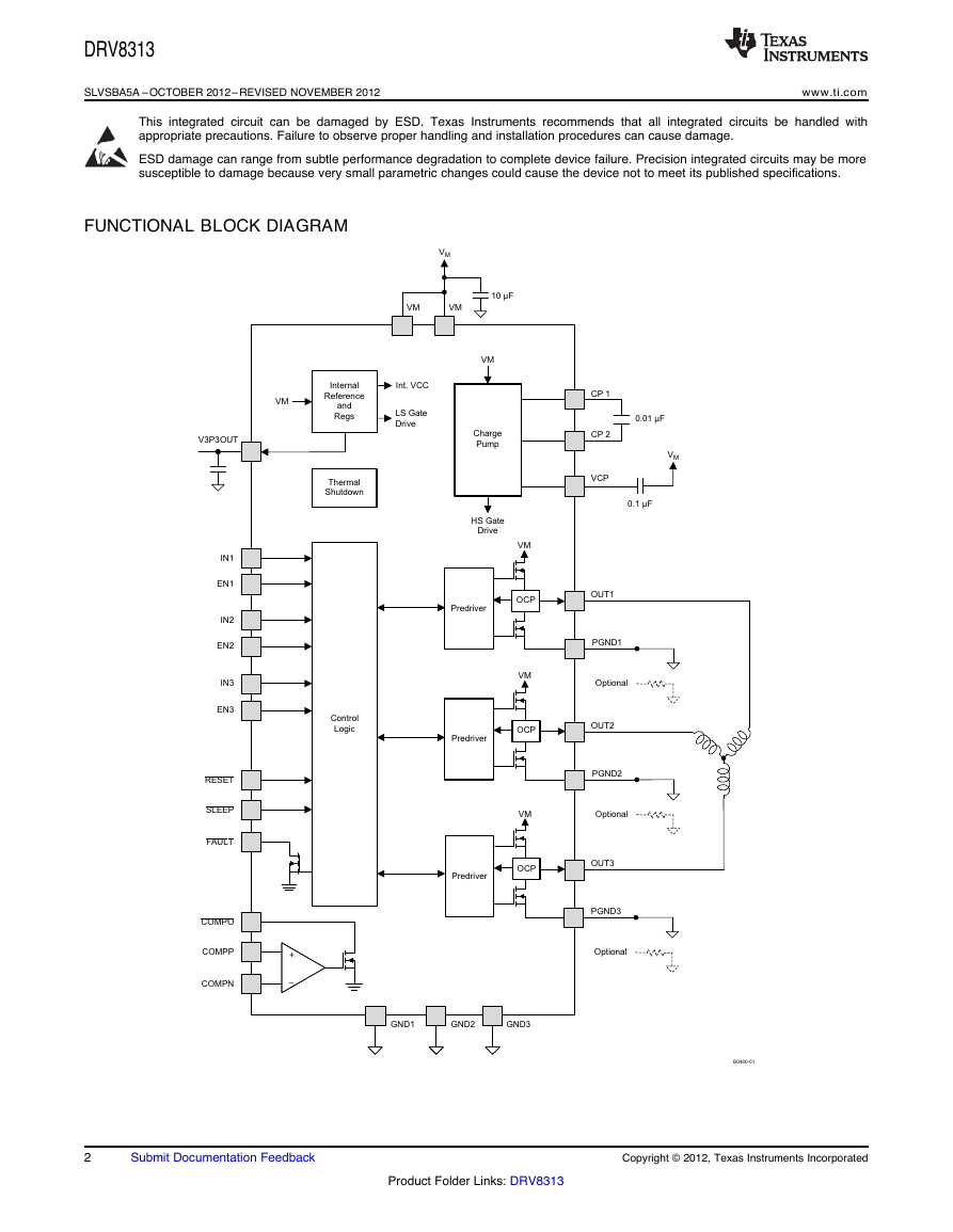
FUNCTIONAL BLOCK DIAGRAM
2
Submit Documentation Feedback
Copyright © 2012, Texas Instruments Incorporated
Product Folder Links: DRV8313
ChargePumpThermalShutdownGND2GND10.01μFVMVMHS GateDriveVMVMInternalReferenceandRegsInt.VCCControlLogicVMVMLS GateDriveVMOUT2Predriver+10μFGND3V3P3OUT0.1μFPredriverPredriverOCPVMOCPVMOCPB0480-01EN1IN2IN3EN3FAULTRESETIN1SLEEPEN2COMPNCOMPOCOMPPOUT1CP1CP2VCPOUT3OptionalOptionalOptionalPGND3PGND2PGND1�
www.ti.com
SLVSBA5A –OCTOBER 2012 –REVISED NOVEMBER 2012
DRV8313
PIN
NAME
NO.
Power and Ground
CP1
CP2
1
2
12, 20, 28,
PPAD
15
3
4, 11
GND
V3P3OUT
VCP
VM
Control
EN1
EN2
EN3
IN1
IN2
IN3
nRESET
nSLEEP
Status
nFAULT
Comparator
COMPN
COMPP
nCOMPO
26
24
22
27
25
23
16
17
18
13
12
19
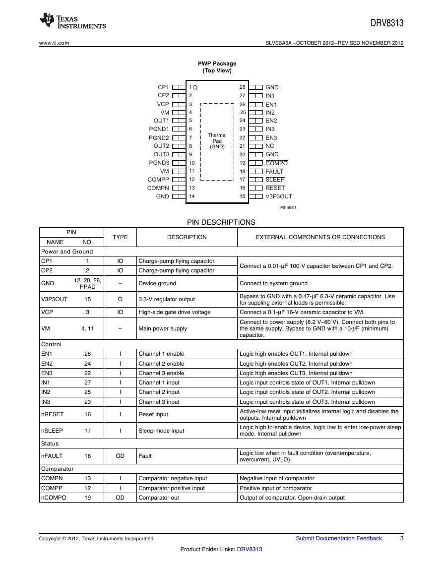
PIN DESCRIPTIONS
TYPE
DESCRIPTION
EXTERNAL COMPONENTS OR CONNECTIONS
IO
IO
–
O
IO
–
I
I
I
I
I
I
I
I
Charge-pump flying capacitor
Charge-pump flying capacitor
Connect a 0.01-μF 100-V capacitor between CP1 and CP2.
Device ground
Connect to system ground
3.3-V regulator output
High-side gate drive voltage
Main power supply
Bypass to GND with a 0.47-μF 6.3-V ceramic capacitor. Use
for suppling external loads is permissible.
Connect a 0.1-μF 16-V ceramic capacitor to VM.
Connect to power supply (8.2 V–60 V). Connect both pins to
the same supply. Bypass to GND with a 10-µF (minimum)
capacitor.
Channel 1 enable
Channel 2 enable
Channel 3 enable
Channel 1 input
Channel 2 input
Channel 3 input
Reset input
Sleep-mode input
Logic high enables OUT1. Internal pulldown
Logic high enables OUT2. Internal pulldown
Logic high enables OUT3. Internal pulldown
Logic input controls state of OUT1. Internal pulldown
Logic input controls state of OUT2. Internal pulldown
Logic input controls state of OUT3. Internal pulldown
Active-low reset input initializes internal logic and disables the
outputs. Internal pulldown
Logic high to enable device, logic low to enter low-power sleep
mode. Internal pulldown
OD
Fault
Logic low when in fault condition (overtemperature,
overcurrent, UVLO)
I
I
OD
Comparator negative input
Comparator positive input
Comparator out
Negative input of comparator
Positive input of comparator
Output of comparator. Open-drain output
Copyright © 2012, Texas Instruments Incorporated
Submit Documentation Feedback
3
Product Folder Links: DRV8313
1234567891113101214ThermalPad(GND)2827262524232221201816191715PWPPackage(Top View)P0146-01CP1CP2VCPVMCOMPNVMOUT1PGND1PGND2OUT2OUT3PGND3COMPPGNDGNDGNDIN1EN1IN2EN2IN3EN3NCCOMPOFAULTSLEEPRESETV3P3OUT�
DRV8313
SLVSBA5A –OCTOBER 2012 –REVISED NOVEMBER 2012
www.ti.com
PIN
NAME
NO.
TYPE
DESCRIPTION
EXTERNAL COMPONENTS OR CONNECTIONS
PIN DESCRIPTIONS (continued)
Output
OUT1
OUT2
OUT3
PGND1
PGND2
PGND3
5
8
9
6
7
10
O
O
O
–
–
–
Output 1
Output 2
Output 3
Ground for OUT1
Ground for OUT2
Ground for OUT3
Connect to loads.
Connect to ground, or to low-side current-sense resistors.
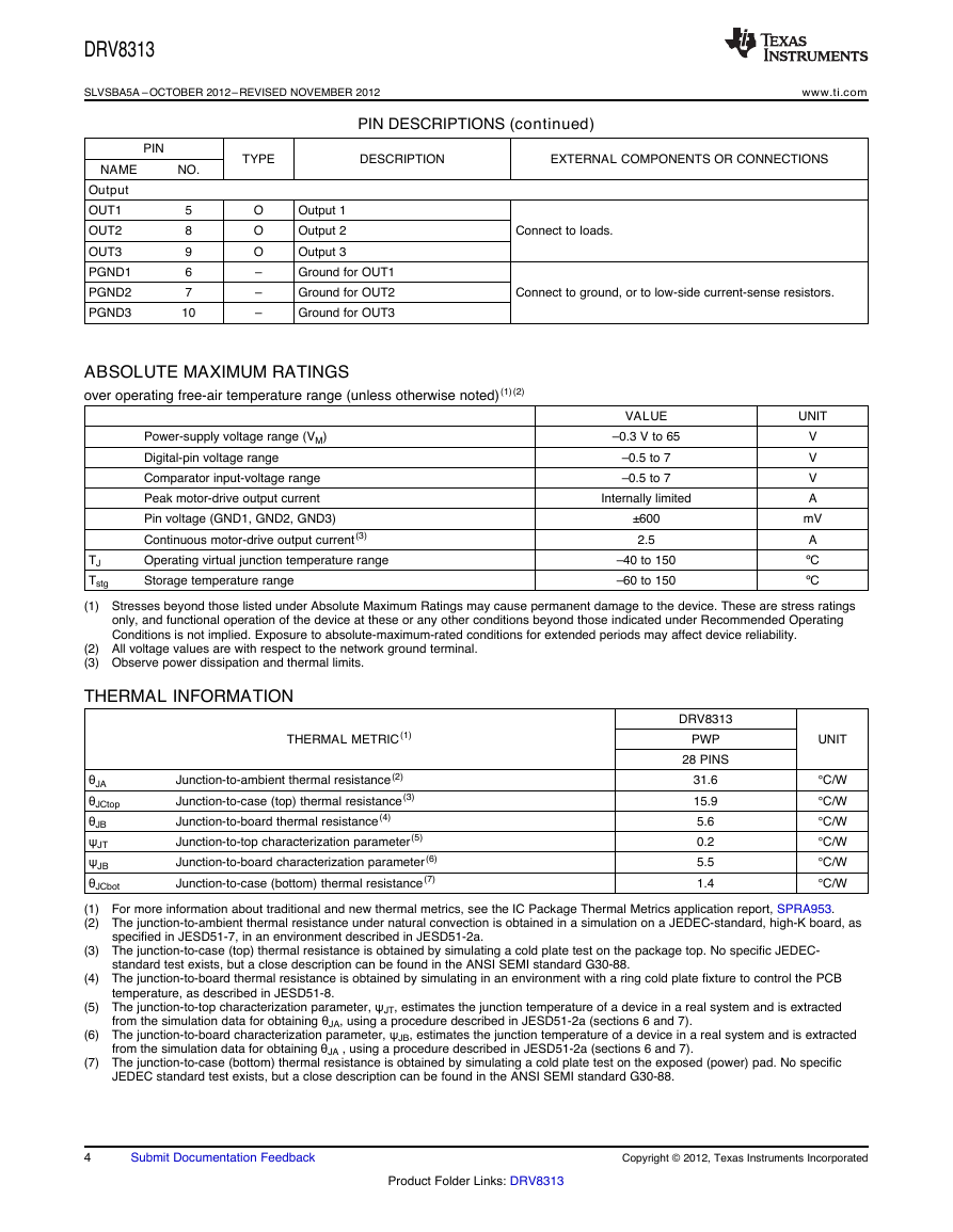
ABSOLUTE MAXIMUM RATINGS
over operating free-air temperature range (unless otherwise noted) (1) (2)
Power-supply voltage range (VM)
Digital-pin voltage range
Comparator input-voltage range
Peak motor-drive output current
Pin voltage (GND1, GND2, GND3)
Continuous motor-drive output current (3)
Operating virtual junction temperature range
Storage temperature range
TJ
Tstg
VALUE
–0.3 V to 65
–0.5 to 7
–0.5 to 7
Internally limited
±600
2.5
–40 to 150
–60 to 150
UNIT
V
V
V
A
mV
A
ºC
ºC
(1) Stresses beyond those listed under Absolute Maximum Ratings may cause permanent damage to the device. These are stress ratings
only, and functional operation of the device at these or any other conditions beyond those indicated under Recommended Operating
Conditions is not implied. Exposure to absolute-maximum-rated conditions for extended periods may affect device reliability.
(2) All voltage values are with respect to the network ground terminal.
(3) Observe power dissipation and thermal limits.
THERMAL INFORMATION
THERMAL METRIC(1)
θJA
θJCtop
θJB
ψJT
ψJB
θJCbot
Junction-to-ambient thermal resistance (2)
Junction-to-case (top) thermal resistance (3)
Junction-to-board thermal resistance (4)
Junction-to-top characterization parameter (5)
Junction-to-board characterization parameter (6)
Junction-to-case (bottom) thermal resistance (7)
DRV8313
PWP
28 PINS
31.6
15.9
5.6
0.2
5.5
1.4
UNIT
°C/W
°C/W
°C/W
°C/W
°C/W
°C/W
(1) For more information about traditional and new thermal metrics, see the IC Package Thermal Metrics application report, SPRA953.
(2) The junction-to-ambient thermal resistance under natural convection is obtained in a simulation on a JEDEC-standard, high-K board, as
specified in JESD51-7, in an environment described in JESD51-2a.
(3) The junction-to-case (top) thermal resistance is obtained by simulating a cold plate test on the package top. No specific JEDEC-
standard test exists, but a close description can be found in the ANSI SEMI standard G30-88.
(4) The junction-to-board thermal resistance is obtained by simulating in an environment with a ring cold plate fixture to control the PCB
temperature, as described in JESD51-8.
(5) The junction-to-top characterization parameter, ψJT, estimates the junction temperature of a device in a real system and is extracted
from the simulation data for obtaining θJA, using a procedure described in JESD51-2a (sections 6 and 7).
(6) The junction-to-board characterization parameter, ψJB, estimates the junction temperature of a device in a real system and is extracted
from the simulation data for obtaining θJA , using a procedure described in JESD51-2a (sections 6 and 7).
(7) The junction-to-case (bottom) thermal resistance is obtained by simulating a cold plate test on the exposed (power) pad. No specific
JEDEC standard test exists, but a close description can be found in the ANSI SEMI standard G30-88.
Spacer
4
Submit Documentation Feedback
Copyright © 2012, Texas Instruments Incorporated
Product Folder Links: DRV8313
�
DRV8313
www.ti.com
SLVSBA5A –OCTOBER 2012 –REVISED NOVEMBER 2012
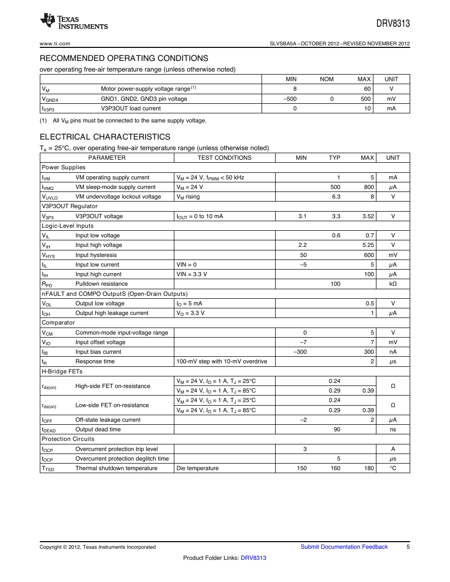
RECOMMENDED OPERATING CONDITIONS
over operating free-air temperature range (unless otherwise noted)
VM
VGNDX
IV3P3
Motor power-supply voltage range (1)
GND1, GND2, GND3 pin voltage
V3P3OUT load current
(1) All VM pins must be connected to the same supply voltage.
MIN
8
–500
0
NOM
0
MAX
60
500
10
UNIT
V
mV
mA
ELECTRICAL CHARACTERISTICS
TA = 25°C, over operating free-air temperature range (unless otherwise noted)
PARAMETER
TEST CONDITIONS
MIN
TYP
MAX
UNIT
VM operating supply current
VM sleep-mode supply current
VM undervoltage lockout voltage
VM = 24 V, fPWM < 50 kHz
VM = 24 V
VM rising
V3P3OUT voltage
IOUT = 0 to 10 mA
Input low voltage
Input high voltage
Input hysteresis
Input low current
Input high current
Pulldown resistance
Power Supplies
IVM
IVMQ
VUVLO
V3P3OUT Regulator
V3P3
Logic-Level Inputs
VIL
VIH
VHYS
IIL
IIH
RPD
nFAULT and COMPO OutputS (Open-Drain Outputs)
VOL
IOH
Comparator
VCM
VIO
IIB
tR
H-Bridge FETs
Common-mode input-voltage range
Input offset voltage
Input bias current
Response time
Output low voltage
Output high leakage current
VIN = 0
VIN = 3.3 V
IO = 5 mA
VO = 3.3 V
100-mV step with 10-mV overdrive
rds(on)
rds(on)
High-side FET on-resistance
Low-side FET on-resistance
VM = 24 V, IO = 1 A, TJ = 25°C
VM = 24 V, IO = 1 A, TJ = 85°C
VM = 24 V, IO = 1 A, TJ = 25°C
VM = 24 V, IO = 1 A, TJ = 85°C
Off-state leakage current
Output dead time
IOFF
tDEAD
Protection Circuits
IOCP
tOCP
TTSD
Overcurrent protection trip level
Overcurrent protection deglitch time
Thermal shutdown temperature
Die temperature
1
500
6.3
3.3
0.6
100
0.24
0.29
0.24
0.29
90
5
160
5
800
8
mA
µA
V
3.52
V
0.7
5.25
600
5
100
0.5
1
5
7
300
2
0.39
0.39
2
180
V
V
mV
µA
µA
kΩ
V
µA
V
mV
nA
µs
Ω
Ω
µA
ns
A
µs
°C
3.1
2.2
50
–5
0
–7
–300
–2
3
150
Copyright © 2012, Texas Instruments Incorporated
Submit Documentation Feedback
5
Product Folder Links: DRV8313
�
DRV8313
SLVSBA5A –OCTOBER 2012 –REVISED NOVEMBER 2012
SWITCHING CHARACTERISTICS(1)
TA = 25°, VM = 24 V, RL = 20 Ω
NO.
PARAMETER
DESCRIPTION
1
2
3
4
5
6
7
8
t1
t2
t3
t4
t5
t6
tr
tf
Delay time, ENx high to OUTx high, INx = 1
Delay time, ENx low to OUTx low, INx = 1
Delay time, ENx high to OUTx low, INx = 0
Delay time, ENx low to OUTx high, INx = 0
Delay time, INx high to OUTx high
Delay time, INx low to OUTx low
Output rise time, resistive load to GND
Output fall time, resistive load to GND
(1) Not production tested
www.ti.com
MIN
130
275
100
200
300
275
30
30
MAX
330
475
300
400
500
475
150
150
UNIT
ns
ns
ns
ns
ns
ns
ns
ns
Figure 1. DRV8313 Switching Characteristics
6
Submit Documentation Feedback
Copyright © 2012, Texas Instruments Incorporated
Product Folder Links: DRV8313
INx = 1, Resistive Load to GNDT0543-0150%80%20%80%20%tftrOUTx50%50%50%t1t2ENxOUTxINx = 0, Resistive Load to VM50%50%50%50%t3t4ENxOUTxENx = 1, Resistive Load to GND50%50%50%50%t5t6INxOUTx�
DRV8313
www.ti.com
SLVSBA5A –OCTOBER 2012 –REVISED NOVEMBER 2012
FUNCTIONAL DESCRIPTION
Output Stage
The DRV8313 contains three half-H-bridge drivers. The source terminals of the low-side FETs of all three half-H-
bridges terminate at separate pins (GND1, GND2, and GND3) to allow the use of a low-side current-sense
resistor on each output, if desired. The user may also connect all three together to a single low-side sense
resistor, or may connect them directly to ground if there is no need for current sensing.
If using a low-side sense resistor, take care to ensure that the voltage on the GND1, GND2, or GND3 pin does
not exceed ±500 mV.
Note that there are multiple VM motor power-supply pins. Connect all VM pins together to the motor-supply
voltage.
Bridge Control
The INx input pins directly control the state (high or low) of the OUTx outputs; the ENx input pins enable or
disable the OUTx driver. The following table shows the logic:
INx
X
0
1
ENx
OUTx
0
1
1
Z
L
H
Charge Pump
Because the output stages use N-channel FETs, the device requires a gate-drive voltage higher than the VM
power supply to enhance the high-side FETs fully. The DRV8313 integrates a charge-pump circuit that generates
a voltage above the VM supply for this purpose.
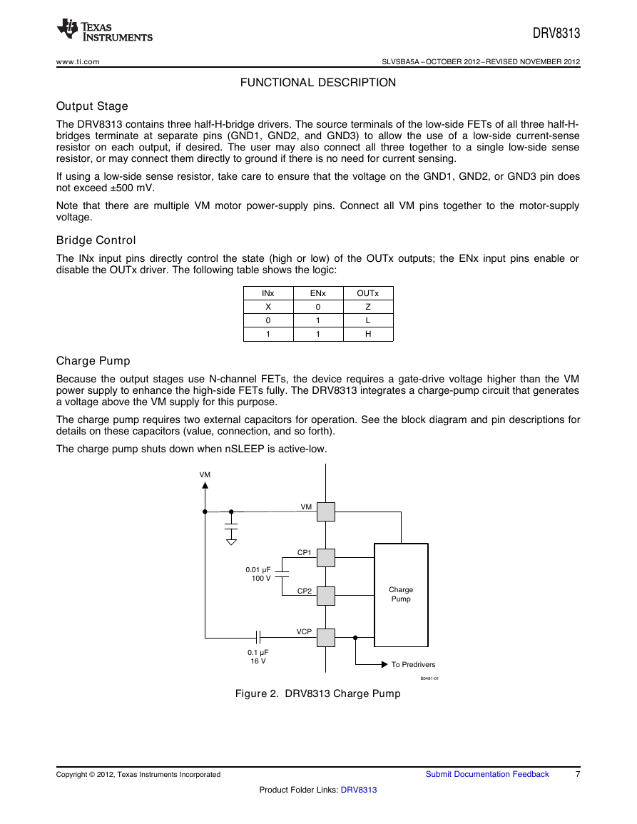
The charge pump requires two external capacitors for operation. See the block diagram and pin descriptions for
details on these capacitors (value, connection, and so forth).
The charge pump shuts down when nSLEEP is active-low.
Figure 2. DRV8313 Charge Pump
Copyright © 2012, Texas Instruments Incorporated
Submit Documentation Feedback
7
Product Folder Links: DRV8313
ChargePump CP1CP2VCPVMVM0.01 F100 V0.1 F16 VTo PredriversB0481-01�
DRV8313
SLVSBA5A –OCTOBER 2012 –REVISED NOVEMBER 2012
www.ti.com
Comparator
The DRV8313 includes an uncommitted comparator, which can find use as a current-limit comparator or for other
purposes.
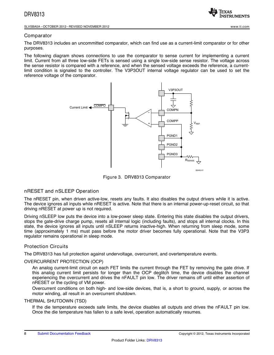
The following diagram shows connections to use the comparator to sense current for implementing a current
limit. Current from all three low-side FETs is sensed using a single low-side sense resistor. The voltage across
the sense resistor is compared with a reference, and when the sensed voltage exceeds the reference, a current-
limit condition is signaled to the controller. The V3P3OUT internal voltage regulator can be used to set the
reference voltage of the comparator.
Figure 3. DRV8313 Comparator
nRESET and nSLEEP Operation
The nRESET pin, when driven active-low, resets any faults. It also disables the output drivers while it is active.
The device ignores all inputs while nRESET is active. Note that there is an internal power-up-reset circuit, so that
driving nRESET at power up is not required.
Driving nSLEEP low puts the device into a low-power sleep state. Entering this state disables the output drivers,
stops the gate-drive charge pump, resets all internal logic (including faults), and stops all internal clocks. In this
state, the device ignores all inputs until nSLEEP returns inactive-high. When returning from sleep mode, some
time (approximately 1 ms) must pass before the motor driver becomes fully operational. Note that the V3P3
regulator remains operational in sleep mode.
Protection Circuits
The DRV8313 has full protection against undervoltage, overcurrent, and overtemperature events.
OVERCURRENT PROTECTION (OCP)
An analog current-limit circuit on each FET limits the current through the FET by removing the gate drive. If
this analog current limit persists for longer than the OCP deglitch time, the device disables the channel
experiencing the overcurrent and drives the nFAULT pin low. The driver remains off until either assertion of
nRESET or the cycling of VM power.
Overcurrent conditions on both high- and low-side devices, that is, a short to ground, supply, or across the
motor winding, all result in an overcurrent shutdown.
THERMAL SHUTDOWN (TSD)
If the die temperature exceeds safe limits, the device disables all outputs and drives the nFAULT pin low.
Once the die temperature has fallen to a safe level, operation automatically resumes.
8
Submit Documentation Feedback
Copyright © 2012, Texas Instruments Incorporated
Product Folder Links: DRV8313
PGND1PGND2PGND3COMPPCOMPOCOMPNCurrentLimitRSENSEVREF+V3P3OUTB0482-01–�




 2023年江西萍乡中考道德与法治真题及答案.doc
 2012年重庆南川中考生物真题及答案.doc
 2013年江西师范大学地理学综合及文艺理论基础考研真题.doc
 2020年四川甘孜小升初语文真题及答案I卷.doc
 2020年注册岩土工程师专业基础考试真题及答案.doc
 2023-2024学年福建省厦门市九年级上学期数学月考试题及答案.doc
 2021-2022学年辽宁省沈阳市大东区九年级上学期语文期末试题及答案.doc
 2022-2023学年北京东城区初三第一学期物理期末试卷及答案.doc
 2018上半年江西教师资格初中地理学科知识与教学能力真题及答案.doc
 2012年河北国家公务员申论考试真题及答案-省级.doc
 2020-2021学年江苏省扬州市江都区邵樊片九年级上学期数学第一次质量检测试题及答案.doc
 2022下半年黑龙江教师资格证中学综合素质真题及答案.doc