Application Report
SPRA524
Space-Vector PWM With
TMS320C24x/F24x Using Hardware and
Software Determined Switching Patterns
Zhenyu Yu
Abstract
Digital Signal Processing Solutions
Space-vector (SV) pulse width modulation (PWM) technique has become a popular PWM
technique for three-phase voltage-source inverters (VSI) in applications such as control of AC
induction and permanent-magnet synchronous motors. This document gives an in-depth
discussion of the theory and implementation of the SV PWM technique.
Two different SV PWM waveform patterns, one using the regular compare function on the Texas
Instruments (TI�) TMS320C24x/F24x digital signal processors (DSPs) and another implemented
with the SV PWM hardware module on the TI TMS320C24x/F24x DSPs are presented, with
complete code examples for the TMS320F243/1. At the end, a complete AC induction motor
control application is discussed to show the effectiveness of both approaches.
PWM waveforms of the presented implementations and experimental data in the form of motor
currents are shown and discussed. A full TMS320F243/1 program example is attached. The
observation of dead band imbalance for the hardware-implemented SVPWM pattern in this report
has not been seen in other publications.
Contents
Introduction ......................................................................................................................................................2
Background......................................................................................................................................................3
Theory of SV PWM Technique..................................................................................................................3
SV PWM Waveform Patterns....................................................................................................................9
Application in Three-Phase AC Induction Motor Control ................................................................................20
Experimental Results .....................................................................................................................................22
Conclusions ...................................................................................................................................................22
References.....................................................................................................................................................24
Appendix A. Program for Open-Loop Three-Phase AC Induction Motor Control With SV PWM Technique
and Constant V/Hz Principle ..........................................................................................................................25
Digital Signal Processing Solutions
March 1999
�
Application Report
SPRA524
Figures
Figure 1. Symmetric and Asymmetric PWM Signals .....................................................................................2
Figure 2. Three-Phase VSI Diagram .............................................................................................................3
Figure 3. The Basic Space Vectors (Normalized w.r.t. Vdc) and Switching States ........................................5
Figure 4. Software Determined SV PWM Waveform Pattern ......................................................................10
Figure 5. Switching Direction for Software Determined SV PWM Pattern...................................................11
Figure 6. SV PWM Outputs With Carrier Filtered Out .................................................................................13
Figure 7. SV PWM Outputs With Carrier Filtered Out and Dead Band Enabled .........................................14
Figure 8. Hardware-Implemented SV PWM Waveform Pattern ..................................................................15
Figure 9. SV PWM Outputs With Carrier Filtered Out .................................................................................19
Figure 10. SV PWM Outputs With Carrier Filtered Out and Dead Band Enabled .........................................19
Figure 11. Program Flow Chart.....................................................................................................................20
Figure 12. Block Diagram of an Open-Loop AC Induction Motor Control System.........................................22
Figure 13. Motor Current and Spectrum Obtained With the Software Approach...........................................23
Figure 14. Motor Current and Spectrum Obtained With the Hardware Approach .........................................23
Table 1. Device On/Off States and Corresponding Outputs of a Three-Phase VSI ........................................4
Table 2. Determination of the Sector of Uout Based on N................................................................................8
Table 3. Hardware and Software Determined SV PWM Switching Pattern Comparison.................................9
Tables
Introduction
Because of advances in solid state power devices and microprocessors, PWM inverters
are becoming more and more popular in today’s motor drives. PWM inverters make it
possible to control both the frequency and magnitude of the voltage and current applied
to a motor. As a result, PWM inverter-powered motor drives offer better efficiency and
higher performance compared to fixed frequency motor drives. The energy that a PWM
inverter delivers to a motor is controlled by PWM signals applied to the gates of the
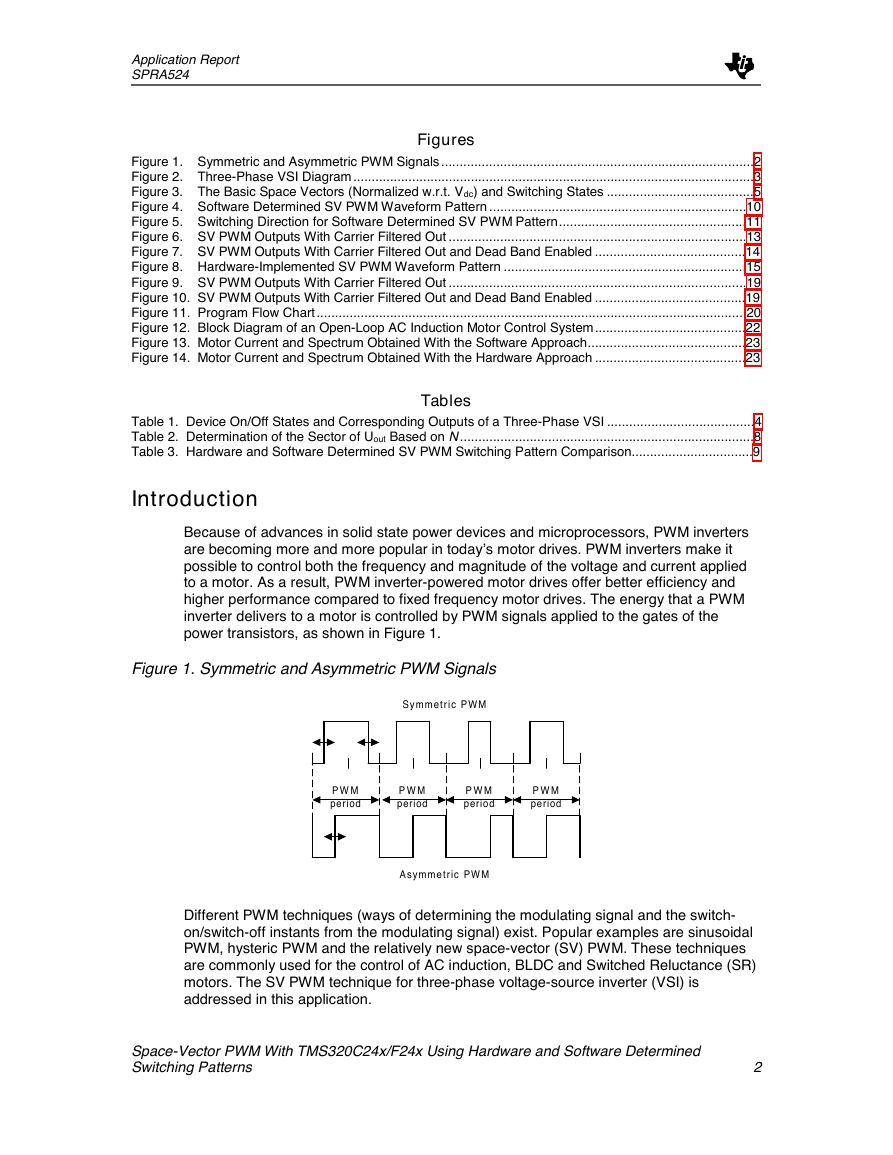
power transistors, as shown in Figure 1.
Figure 1. Symmetric and Asymmetric PWM Signals
Symmetric PWM
P W M
period
P W M
period
P W M
period
P W M
period
Asymmetric PWM
Different PWM techniques (ways of determining the modulating signal and the switch-
on/switch-off instants from the modulating signal) exist. Popular examples are sinusoidal
PWM, hysteric PWM and the relatively new space-vector (SV) PWM. These techniques
are commonly used for the control of AC induction, BLDC and Switched Reluctance (SR)
motors. The SV PWM technique for three-phase voltage-source inverter (VSI) is
addressed in this application.
Space-Vector PWM With TMS320C24x/F24x Using Hardware and Software Determined
Switching Patterns
2
�
Application Report
SPRA524
Background
Theory of SV PWM Technique
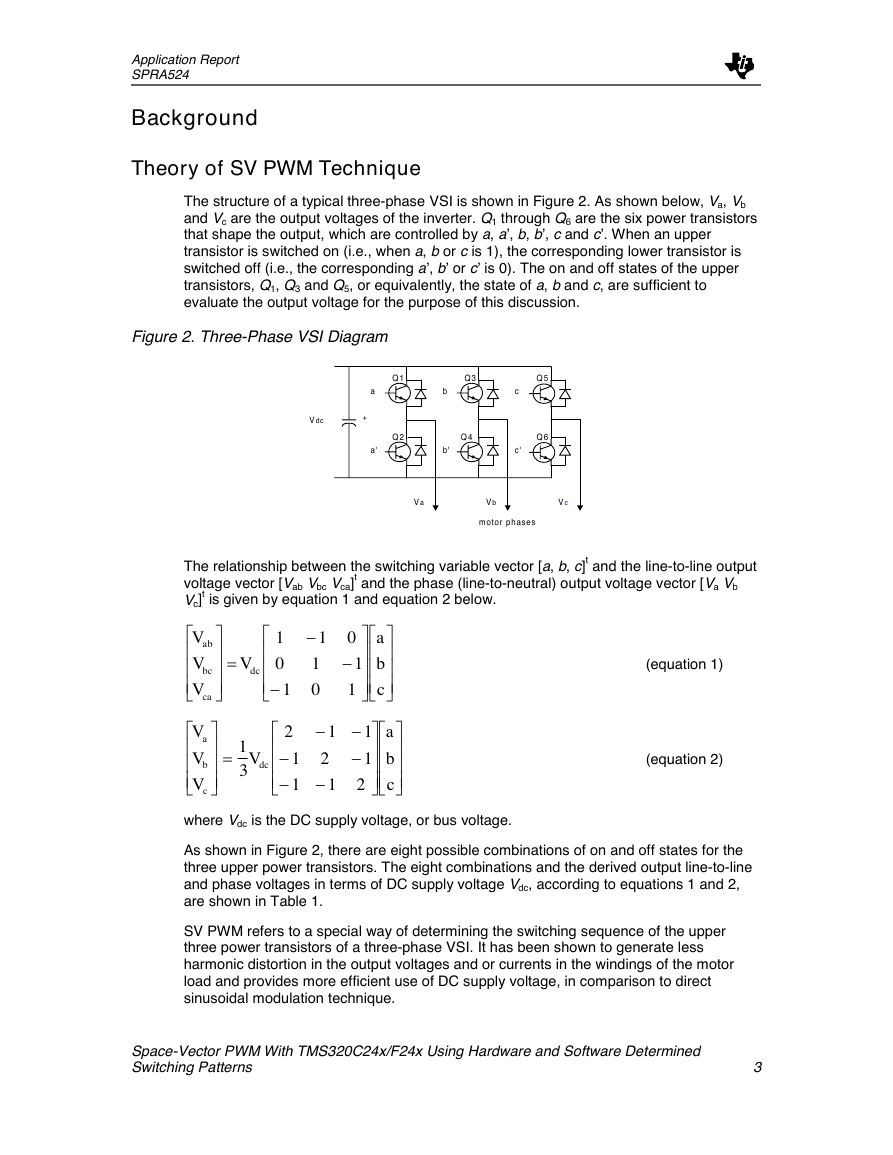
The structure of a typical three-phase VSI is shown in Figure 2. As shown below, Va, Vb
and Vc are the output voltages of the inverter. Q1 through Q6 are the six power transistors
that shape the output, which are controlled by a, a’, b, b’, c and c’. When an upper
transistor is switched on (i.e., when a, b or c is 1), the corresponding lower transistor is
switched off (i.e., the corresponding a’, b’ or c’ is 0). The on and off states of the upper
transistors, Q1, Q3 and Q5, or equivalently, the state of a, b and c, are sufficient to
evaluate the output voltage for the purpose of this discussion.
Figure 2. Three-Phase VSI Diagram
V dc
+
Q 1
Q 2
a
a'
Q 3
Q 4
b
b'
Q 5
Q 6
c
c'
V a
V b
V c
motor phases
The relationship between the switching variable vector [a, b, c]t and the line-to-line output
voltage vector [Vab Vbc Vca]t and the phase (line-to-neutral) output voltage vector [Va Vb
Vc]t is given by equation 1 and equation 2 below.
Ø
V
ab
Œ
V
Œ
bc
Œ
V
º
ca
ø
œ
œ
œ
ß
Ø
V
a
Œ
V
Œ
b
Œ
V
º
c
ø
œ
œ
œ
ß
=
V
dc
Ø
Œ
Œ
Œ
º
1
0
-
1
-
1
1
0
ø
0
œ
-
1
œ
œ
1
ß
Ø
Œ
Œ
Œ
º
a
b
c
ø
œ
œ
œ
ß
=
1
3
V
dc
Ø
Œ
Œ
Œ
º
2
-
1
-
1
-
1
2
-
1
-
-
ø
1
œ
1
œ
œ
2
ß
Ø
Œ
Œ
Œ
º
a
b
c
ø
œ
œ
œ
ß
(equation 1)
(equation 2)
where Vdc is the DC supply voltage, or bus voltage.
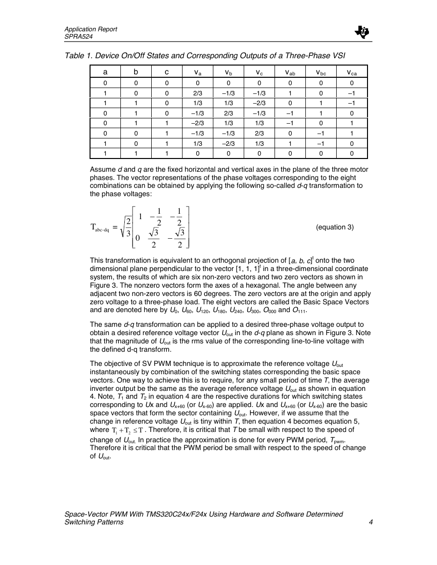
As shown in Figure 2, there are eight possible combinations of on and off states for the
three upper power transistors. The eight combinations and the derived output line-to-line
and phase voltages in terms of DC supply voltage Vdc, according to equations 1 and 2,
are shown in Table 1.
SV PWM refers to a special way of determining the switching sequence of the upper
three power transistors of a three-phase VSI. It has been shown to generate less
harmonic distortion in the output voltages and or currents in the windings of the motor
load and provides more efficient use of DC supply voltage, in comparison to direct
sinusoidal modulation technique.
Space-Vector PWM With TMS320C24x/F24x Using Hardware and Software Determined
Switching Patterns
3
�
Application Report
SPRA524
Table 1. Device On/Off States and Corresponding Outputs of a Three-Phase VSI
a
0
1
1
0
0
0
1
1
b
0
0
1
1
1
0
0
1
c
0
0
0
0
1
1
1
1
va
0
2/3
1/3
–1/3
–2/3
–1/3
1/3
0
vb
0
–1/3
1/3
2/3
1/3
–1/3
–2/3
0
vc
0
–1/3
–2/3
–1/3
1/3
2/3
1/3
0
vab
0
1
0
–1
–1
0
1
0
vbc
0
0
1
1
0
–1
–1
0
vca
0
–1
–1
0
1
1
0
0
Assume d and q are the fixed horizontal and vertical axes in the plane of the three motor
phases. The vector representations of the phase voltages corresponding to the eight
combinations can be obtained by applying the following so-called d-q transformation to
the phase voltages:
abcT
=dq-
2
3
Ø
Œ
Œ
Œ
Œ
º
1
0
-
1
2
3
2
-
-
1
2
3
2
ø
œ
œ
œ
œ
ß
(equation 3)
This transformation is equivalent to an orthogonal projection of [a, b, c]t onto the two
dimensional plane perpendicular to the vector [1, 1, 1]t in a three-dimensional coordinate
system, the results of which are six non-zero vectors and two zero vectors as shown in
Figure 3. The nonzero vectors form the axes of a hexagonal. The angle between any
adjacent two non-zero vectors is 60 degrees. The zero vectors are at the origin and apply
zero voltage to a three-phase load. The eight vectors are called the Basic Space Vectors
and are denoted here by U0, U60, U120, U180, U240, U300, O000 and O111.
The same d-q transformation can be applied to a desired three-phase voltage output to
obtain a desired reference voltage vector Uout in the d-q plane as shown in Figure 3. Note
that the magnitude of Uout is the rms value of the corresponding line-to-line voltage with
the defined d-q transform.
The objective of SV PWM technique is to approximate the reference voltage Uout
instantaneously by combination of the switching states corresponding the basic space
vectors. One way to achieve this is to require, for any small period of time T, the average
inverter output be the same as the average reference voltage Uout as shown in equation
4. Note, T1 and T2 in equation 4 are the respective durations for which switching states
corresponding to Ux and Ux+60 (or Ux-60) are applied. Ux and Ux+60 (or Ux-60) are the basic
space vectors that form the sector containing Uout. However, if we assume that the
change in reference voltage Uout is tiny within T, then equation 4 becomes equation 5,
where
change of Uout. In practice the approximation is done for every PWM period, Tpwm.
Therefore it is critical that the PWM period be small with respect to the speed of change
of Uout.
. Therefore, it is critical that T be small with respect to the speed of
T
2
�
T
T
1
�
Space-Vector PWM With TMS320C24x/F24x Using Hardware and Software Determined
Switching Patterns
4
�
Application Report
SPRA524
Figure 3. The Basic Space Vectors (Normalized w.r.t. Vdc) and Switching States
U 12 0
(010)
q
axis
(
� 1
6 1
,
)
2
U 60
(110)
(
1
6 1
,
)
2
U 180
(011)
(
� 2
3 0,
)
T 1
U out
T 2
O 000
(000)
O 111
(111)
U 0
(100)
(
2
d
axis
)
3 0,
(
�
1
6
,
�
1
)
2
U 240
(001)
U 300
(101)
(
1
6
, �
1
)
2
=
1
T
(
UT
1
x
+
UT
2
)
x
�
60
(
n
1
T
)1
T
�
)(
tU
out
nT
U
out
(
nT
)
=
1
T
(
UT
1
x
+
UT
2
)
x
�
60
(equation 4)
(equation 5)
Equation 5 means that for every PWM period, Uout can be approximated by having the
inverter in switching states Ux and Ux+60 (or Ux-60) for T1 and T2 duration of time
respectively. Since the sum of T1 and T2 should be less than or equal to Tpwm, the inverter
needs to be in O000 or O111 state for the rest of the period. Therefore, equation 5 becomes
equation 6 in the following, where T
1
=T.
T
2
T
o
+
+
=
T
pwm
T U
pwm
out
=
T U
1
x
+
T U
2
x
�
60
+
T
0
(
0
000
or
0
111
)
(equation 6)
From equation 6, we get equation 7 for T1 and T2.
[
T
1
]
=J
T
T
2
pwm
[
UU
x
x
�
60
1
�
]
U
out
(equation 7)
where [
x UU
�x
60
�
] 1
is the normalized decomposition matrix for the sector.
Assume the angle between Uout and Ux is a . From Figure 3, we can also obtain equation
8 in the following for T1 and T2.
=
=
T
1
T
2
2
T
pwm
U
out
cos(
a
+
)30
2
T
pwm
U
out
sin(
a
)
(equation 8)
Depending on specific application, calculation of T1 and T2 can be done either with
equation 7 or equation 8. Equation 7 is sector dependent. However, the matrix inverse
can be calculated off-line for each sector and obtained via a look-up table during on-line
calculation. This approach is useful when Uout is given in the form of vector [Ud, Uq]t.
Equation 8 is independent of sector and is useful when Uout is given in the form of
magnitude and phase angle.
Space-Vector PWM With TMS320C24x/F24x Using Hardware and Software Determined
Switching Patterns
5
�
Application Report
SPRA524
Ux can be the closest basic space vector on either side of Uout. Ux+60 (or Ux-60) is then the
basic space vector on the opposite side. In either case, T1 represents the component on
Ux, T2 represents the component on the other basic space vector.
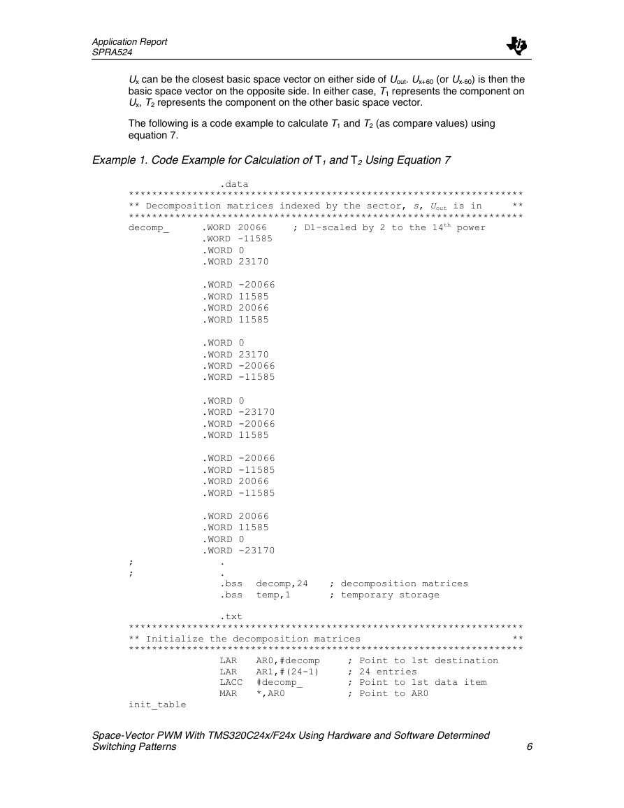
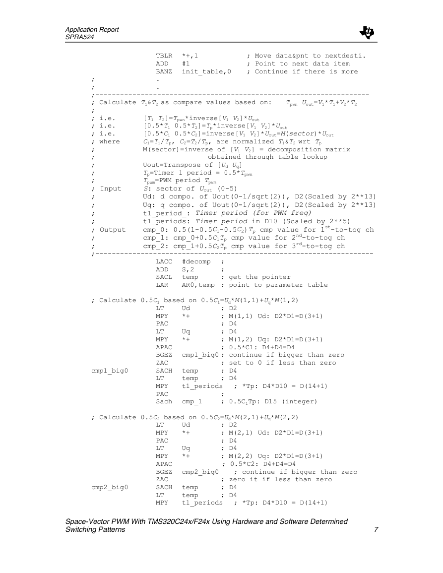
The following is a code example to calculate T1 and T2 (as compare values) using
equation 7.
Example 1. Code Example for Calculation of T1 and T2 Using Equation 7
.data
********************************************************************
** Decomposition matrices indexed by the sector, s, Uout is in
**
********************************************************************
decomp_
; D1–scaled by 2 to the 14th power
.WORD 20066
.WORD -11585
.WORD 0
.WORD 23170
.WORD -20066
.WORD 11585
.WORD 20066
.WORD 11585
.WORD 0
.WORD 23170
.WORD -20066
.WORD -11585
.WORD 0
.WORD -23170
.WORD -20066
.WORD 11585
.WORD -20066
.WORD -11585
.WORD 20066
.WORD -11585
.WORD 20066
.WORD 11585
.WORD 0
.WORD -23170
;
;
.
.
.bss
.bss
.txt
decomp,24
temp,1
; decomposition matrices
; temporary storage
********************************************************************
** Initialize the decomposition matrices
**
********************************************************************
LAR
LAR
LACC
MAR
AR0,#decomp
AR1,#(24-1)
#decomp_
*,AR0
; Point to 1st destination
; 24 entries
; Point to 1st data item
; Point to AR0
init_table
Space-Vector PWM With TMS320C24x/F24x Using Hardware and Software Determined
Switching Patterns
6
�
Application Report
SPRA524
TBLR
ADD
BANZ
.
.
*+,1
#1
init_table,0
; Move data&pnt to nextdesti.
; Point to next data item
; Continue if there is more
Tpwn Uout=V1*T1+V2*T2
[T1 T2]=Tpwn*inverse[V1 V2]*Uout
[0.5*T1 0.5*T2]=Tp*inverse[V1 V2]*Uout
[0.5*C1 0.5*C2]=inverse[V1 V2]*Uout=M(sector)*Uout
C1=T1/Tp, C2=T2/Tp, are normalized T1&T2 wrt Tp
M(sector)=inverse of [V1 V2] = decomposition matrix
;
;
;-------------------------------------------------------------------
; Calculate T1&T2 as compare values based on:
;
; i.e.
; i.e.
; i.e.
; where
;
;
;
;
;
; Input
; Ud: d compo. of Uout(0-1/sqrt(2)), D2(Scaled by 2**13)
; Uq: q compo. of Uout(0-1/sqrt(2)), D2(Scaled by 2**13)
;
;
; Output cmp_0: 0.5(1-0.5C1-0.5C2)Tp cmp value for 1st-to-tog ch
;
;
;--------------------------------------------------------------------
cmp_1: cmp_0+0.5C1Tp cmp value for 2nd-to-tog ch
cmp_2: cmp_1+0.5C2Tp cmp value for 3rd-to-tog ch
Uout=Transpose of [Ud Uq]
Tp=Timer 1 period = 0.5*Tpwm
Tpwm=PWM period Tpwm
S: sector of Uout (0-5)
t1_period_: Timer period (for PWM freq)
t1_periods: Timer period in D10 (Scaled by 2**5)
obtained through table lookup
LACC
ADD
SACL
LAR
#decomp
S,2
temp
AR0,temp ; point to parameter table
;
;
; get the pointer
; Calculate 0.5C1 based on 0.5C1=Ud*M(1,1)+Uq*M(1,2)
; D2
; M(1,1) Ud: D2*D1=D(3+1)
; D4
; D4
; M(1,2) Uq: D2*D1=D(3+1)
; 0.5*C1: D4+D4=D4
cmp1_big0 ; continue if bigger than zero
; set to 0 if less than zero
; D4
; D4
temp
temp
t1_periods
;
; 0.5C1Tp: D15 (integer)
; *Tp: D4*D10 = D(14+1)
cmp_1
LT
MPY
PAC
LT
MPY
APAC
BGEZ
ZAC
SACH
LT
MPY
PAC
Sach
Ud
*+
Uq
*+
Uq
*+
cmp1_big0
cmp2_big0
; Calculate 0.5C2 based on 0.5C2=Ud*M(2,1)+Uq*M(2,2)
Ud
*+
; D2
; M(2,1) Ud: D2*D1=D(3+1)
; D4
; D4
; M(2,2) Uq: D2*D1=D(3+1)
LT
MPY
PAC
LT
MPY
APAC ; 0.5*C2: D4+D4=D4
BGEZ
ZAC
SACH
LT
MPY
; zero it if less than zero
; D4
; D4
temp
temp
t1_periods
; *Tp: D4*D10 = D(14+1)
cmp2_big0
; continue if bigger than zero
Space-Vector PWM With TMS320C24x/F24x Using Hardware and Software Determined
Switching Patterns
7
�
Application Report
SPRA524
PAC
Sach
cmp_2
;
; 0.5C2Tp: D15 (integer)
; Calculate compare value 3 based on 0.5C0Tp=(1-0.5C1-0.5C2)Tp
LACC
SUB
SUB
BGEZ
ZAC
sfr
SACH
cmp0_big0
#t1_period_ ; Calculate 0.5*C0
cmp_1
cmp_2
cmp0_big0
;
; 0.5*C0Tp = (1-0.5*C1 -0.5*C2)Tp: D15
; continue if bigger than zero
; zero it if less than zero
; divide by 2
; 0.25*C0Tp: D15 (integer)
cmp_0
Note that the D scaling notation is equivalent to the more popular Q notation. Their
relationship is Qx=D(15-x). Therefore, the notation Dx means that the decimal point is at
bit[15-x]. Whenever possible, the code examples in this report use maximum scaling to
increase resolution and accuracy. For example, since the range of phase angle, G, is 0 to
2*pi (or 0 to 6.283), it is designated as a D3 (or Q12) number for maximum resolution.
Therefore the digital representation, Gd, for G is related to G by Gd=G*212, i.e., scaled up by
2 to the 12th power.
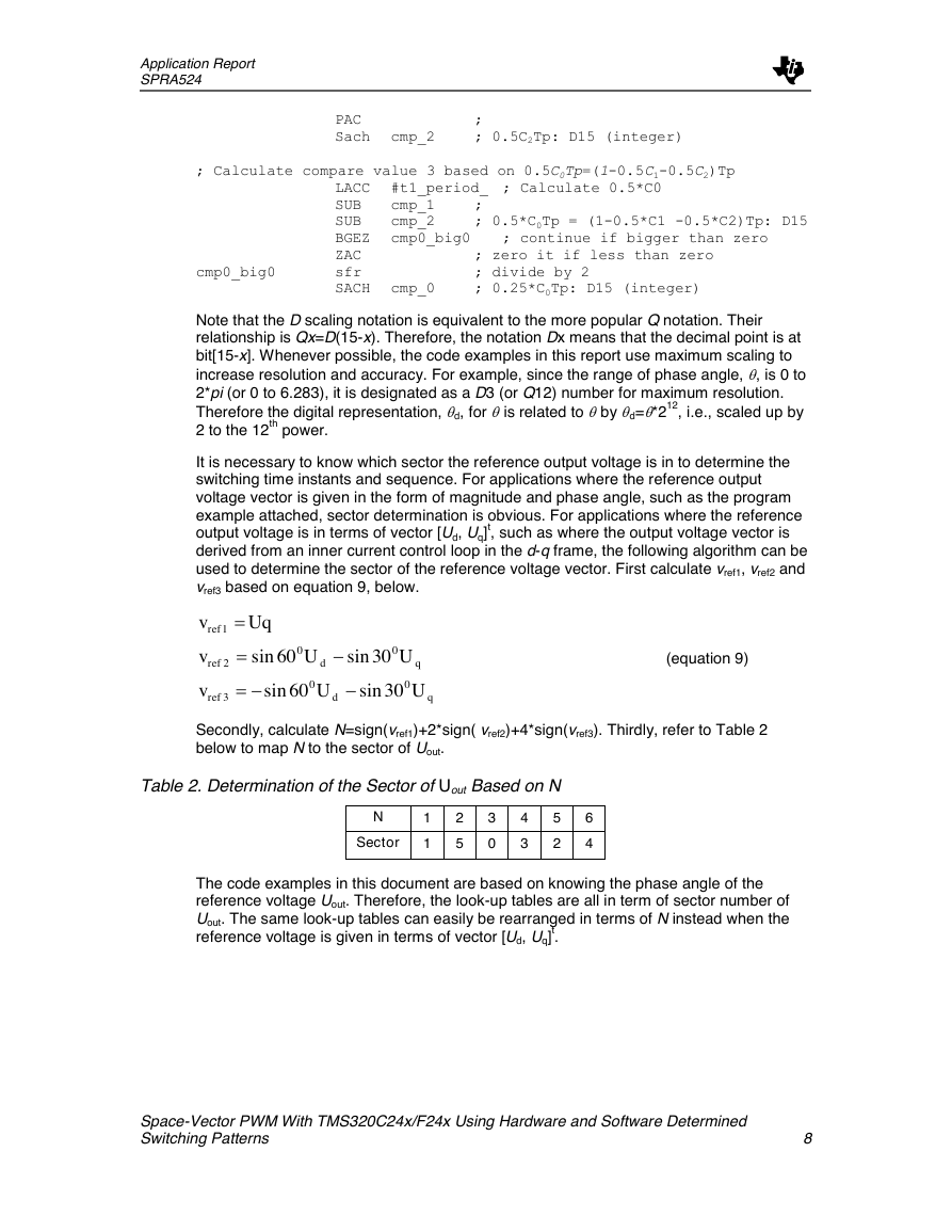
It is necessary to know which sector the reference output voltage is in to determine the
switching time instants and sequence. For applications where the reference output
voltage vector is given in the form of magnitude and phase angle, such as the program
example attached, sector determination is obvious. For applications where the reference
output voltage is in terms of vector [Ud, Uq]t, such as where the output voltage vector is
derived from an inner current control loop in the d-q frame, the following algorithm can be
used to determine the sector of the reference voltage vector. First calculate vref1, vref2 and
vref3 based on equation 9, below.
v
v
v
ref
1
ref
2
ref
3
=
Uq
=
sin
60
0
-=
sin
60
0
U
d
U
sin
-
-
d
0
30
U
sin
0
30
q
(equation 9)
q
U
Secondly, calculate N=sign(vref1)+2*sign( vref2)+4*sign(vref3). Thirdly, refer to Table 2
below to map N to the sector of Uout.
Table 2. Determination of the Sector of Uout Based on N
N
Sector
1
1
2
5
3
0
4
3
5
2
6
4
The code examples in this document are based on knowing the phase angle of the
reference voltage Uout. Therefore, the look-up tables are all in term of sector number of
Uout. The same look-up tables can easily be rearranged in terms of N instead when the
reference voltage is given in terms of vector [Ud, Uq]t.
Space-Vector PWM With TMS320C24x/F24x Using Hardware and Software Determined
Switching Patterns
8
�




 2023年江西萍乡中考道德与法治真题及答案.doc
 2012年重庆南川中考生物真题及答案.doc
 2013年江西师范大学地理学综合及文艺理论基础考研真题.doc
 2020年四川甘孜小升初语文真题及答案I卷.doc
 2020年注册岩土工程师专业基础考试真题及答案.doc
 2023-2024学年福建省厦门市九年级上学期数学月考试题及答案.doc
 2021-2022学年辽宁省沈阳市大东区九年级上学期语文期末试题及答案.doc
 2022-2023学年北京东城区初三第一学期物理期末试卷及答案.doc
 2018上半年江西教师资格初中地理学科知识与教学能力真题及答案.doc
 2012年河北国家公务员申论考试真题及答案-省级.doc
 2020-2021学年江苏省扬州市江都区邵樊片九年级上学期数学第一次质量检测试题及答案.doc
 2022下半年黑龙江教师资格证中学综合素质真题及答案.doc