logo资料库

Radio frequency transistors: principles and practical applicatio....pdf

第1页 / 共317页
第2页 / 共317页
第3页 / 共317页
第4页 / 共317页
第5页 / 共317页
第6页 / 共317页
第7页 / 共317页
第8页 / 共317页
资料共317页,剩余部分请下载后查看
CONTENTS
1 Understanding RF Data Sheet Parameters
1 INTRODUCTION
D.C. SPECIFICATIONS
MAXIMUM RATINGS AND THERMAL CHARACTERISTICS
POWER TRANSISTORS: FUNCTIONAL CHARACTERISTICS
LOW POWER TRANSISTORS: FUNCTIONAL CHARACTERISTICS
LINEAR MODULES: FUNCTIONAL CHARACTERISTICS
POWER MODULES: FUNCTIONAL CHARACTERISTICS
DATA SHEETS OF THE FUTURE
2 RF Transistor Fundamentals
TRANSISTOR CHARACTERISTICS IN SPECIFIC APPLICATIONS
BANDWIDTH CONSIDERATIONS IN SELECTING TRANSISTORS
MOSFETs VERSUS BIPOLARS IN SELECTING A TRANSISTOR
WHATÌS DIFFERENT ABOUT RF TRANSISTORS?
OTHER FACTORS IN RF POWER TRANSISTOR SELECTION
3 FETs and BJTs: Comparison of Parameters and Circuitry
TYPES OF TRANSISTORS
COMPARING THE PARAMETERS
CIRCUIT CONFIGURATIONS
COMMON EMITTER AND COMMON SOURCE
COMMON BASE AND COMMON GATE
COMMON COLLECTOR AND COMMON DRAIN
4 Other Factors Affecting Amplifier Design
CLASSES OF OPERATION
FORMS OF MODULATION
BIASING TO LINEAR OPERATION
OPERATING TRANSISTORS IN A PULSE MODE
5 Reliability Considerations
DIE TEMPERATURE AND ITS EFFECT ON RELIABILITY
OTHER RELIABILITY CONSIDERATIONS
6 Construction Techniques
TYPES OF PACKAGES
THE EMITTER/SOURCE INDUCTANCE
LAYING OUT A CIRCUIT BOARD
TIPS FOR SYSTEMATIC PC LAYOUT DESIGN
MOUNTING RF DEVICES
RF MODULES
7 Power Amplifier Design
STABILITY CONSIDERATIONS
INDUCTORS
MODELING CAPACITORS AT LOW IMPEDANCES
THE INPUT IMPEDANCE OF A HIGH POWER RF TRANSISTOR
THE FIRST MATCHING ELEMENT: A SHUNT C
CAPACITORS AT RADIO FREQUENCIES
COMPONENT CONSIDERATIONS
A PRACTICAL DESIGN EXAMPLE OF A SINGLE STAGE
INTERSTAGE IMPEDANCE MATCHING
IMPEDANCES AND MATCHING NETWORKS
PUSH-PULL AMPLIFIERS
MOSFETs
PARALLEL TRANSISTOR AMPLIFIERS: BIPOLAR TRANSISTORS
QUASI-LUMPED ELEMENT REALIZATION
DISTRIBUTED CIRCUIT REALIZATION
SINGLE-ENDED RF AMPLIFIER DESIGNS: LUMPED CIRCUIT REALIZATION
SINGLE-ENDED, PARALLEL, OR PUSH-PULL
8 Computer-Aided Design Programs
8 GENERAL
INSIDE MOTOROLAÌS IMPEDANCE MATCHING PROGRAM
MIMP DESCRIPTION
SMITH CHARTS AND MIMP
9 After the Power Amplifier
VSWR PROTECTION OF SOLID STATE AMPLIFIERS
TESTING THE CIRCUIT
OUTPUT FILTERING
TYPES OF LOW PASS FILTERS
THE DESIGN PROCEDURE
THE COMPONENTS
10 Wideband Impedance Matching
INTRODUCTION TO WIDEBAND CIRCUITS
CONVENTIONAL TRANSFORMERS
TWISTED WIRE TRANSFORMERS
TRANSMISSION LINE TRANSFORMERS
EQUAL DELAY TRANSMISSION LINE TRANSFORMERS
11 Powewr Splitting and Combining
11 INTRODUCTION
BASIC TYPES OF POWER COMBINERS
IN-PHASE AND 180 COMBINERS
90 HYBRIDS
LINE HYBRIDS
RING HYBRIDS
BRANCH LINE COUPLERS
WILKINSON COUPLERS
12 Frequency Compensation and Negative Feedback
FREQUENCY COMPENSATION
NEGATIVE FEEDBACK
13 Small Signal Amplifier Design
SCATTERING PARAMETERS
NOISE PARAMETERS
BIASING CONSIDERATIONS
POWER GAIN
STABILITY
SUMMARY OF GAIN/NOISE FIGURE DESIGN PROCEDURES
ACTUAL STEPS IN LOW POWER AMPLIFIER DESIGN
DETERMINING DESIRED VALUES OF SOURCE AND LOAD IMPEDANCES
CIRCUIT REALIZATION
14 LDMOS RF Power Transistors and Their Applications
14 INTRODUCTION
LDMOSFET VERSUS VERTICAL MOSFET
DEVICE DESIGN
LDMOS CHARACTERISTICS
LDMOS TRANSISTORS FOR RF POWER APPLICATIONS
SOME FET APPROXIMATIONS
APPLICATIONS OF LDMOS TRANSISTORS IN CURRENT GENERATION CELLULAR TECHNOLOGIES
RF POWER AMPLIFIER CHARACTERISTICS
PRACTICAL EXAMPLE OF DESIGNING A W-CDMA POWER AMPLIFIER
CIRCUIT TECHNIQUES FOR DESIGNING OPTIMUM CDMA AMPLIFIERS
MODELING OF LDMOS TRANSISTORS
COMMENTS
Index
10500_00_i-xvi_7jb.qxd 11/20/00 2:55 PM Page i Radio Frequency Transistors 1 2 3 4 5 6 7 8 9 10 11 12 13 14 15 16 17 18 19 20 21 22 23 24 25 26 27 28 29 30 31 32 33 34 35 36 37 38 39 40 41 42 43 44 45Short 46Reg
10500_00_i-xvi_7jb.qxd 11/20/00 2:55 PM Page ii 1 2 3 4 5 6 7 8 9 10 11 12 13 14 15 16 17 18 19 20 21 22 23 24 25 26 27 28 29 30 31 32 33 34 35 36 37 38 39 40 41 42 43 44 Short45 Reg46
10500_00_i-xvi_7jb.qxd 11/20/00 2:55 PM Page iii Radio Frequency Transistors Principles and Practical Applications Second Edition Norman Dye Helge Granberg Boston Oxford Johannesburg Melbourne New Delhi 1 2 3 4 5 6 7 8 9 10 11 12 13 14 15 16 17 18 19 20 21 22 23 24 25 26 27 28 29 30 31 32 33 34 35 36 37 38 39 40 41 42 43 44 45Short 46Reg
10500_00_i-xvi_7jb.qxd 11/20/00 2:55 PM Page iv Newnes is an imprint of Butterworth–Heinemann. Copyright © 2001 by Butterworth–Heinemann A member of the Reed Elsevier group All rights reserved. No part of this publication may be reproduced, stored in a retrieval system, or transmitted in any form or by any means, electronic, mechanical, photocopying, recording, or otherwise, without the prior written permission of the publisher. Recognizing the importance of preserving what has been written, Butterworth– Heinemann prints its books on acid-free paper whenever possible. Butterworth–Heinemann supports the efforts of American Forests and the Global ReLeaf program in its campaign for the betterment of trees, forests, and our environment. Library of Congress Cataloging-in-Publication Data Dye, Norm, 1929– Radio frequency transistors : principles and practical applications / Norman Dye, Helge Granberg.—2nd ed. p. cm. Includes bibliographical references and index. ISBN 0-7506-7281-1 (pbk. : alk. paper) 1. Power transistors. 2. Transistor amplifiers. 3. Transistor radio transmitters. Helge, 1932– II. Title. 4. Amplifiers, Radio frequency. I. Granberg, TK7871.92 .D96 2000 621.384'12—dc21 00-045618 British Library Cataloguing-in-Publication Data A catalogue record for this book is available from the British Library. The publisher offers special discounts on bulk orders of this book. For information, please contact: Manager of Special Sales Butterworth-Heinemann 225 Wildwood Avenue Woburn, MA 01801-2041 Tel: 781-904-2500 Fax: 781-904-2620 For information on all Newnes publications available, contact our World Wide Web home page at: http://www.newnespress.com 10 9 8 7 6 5 4 3 2 1 Printed in the United States of America 1 2 3 4 5 6 7 8 9 10 11 12 13 14 15 16 17 18 19 20 21 22 23 24 25 26 27 28 29 30 31 32 33 34 35 36 37 38 39 40 41 42 43 44 Short45 Reg46
10500_00_i-xvi_7jb.qxd 11/20/00 2:55 PM Page v Dedicated to the memory of Helge Granberg, who died suddenly in January, 1996 1 2 3 4 5 6 7 8 9 10 11 12 13 14 15 16 17 18 19 20 21 22 23 24 25 26 27 28 29 30 31 32 33 34 35 36 37 38 39 40 41 42 43 44 45Short 46Reg
10500_00_i-xvi_7jb.qxd 11/20/00 2:55 PM Page vi 1 2 3 4 5 6 7 8 9 10 11 12 13 14 15 16 17 18 19 20 21 22 23 24 25 26 27 28 29 30 31 32 33 34 35 36 37 38 39 40 41 42 43 44 Short45 Reg46
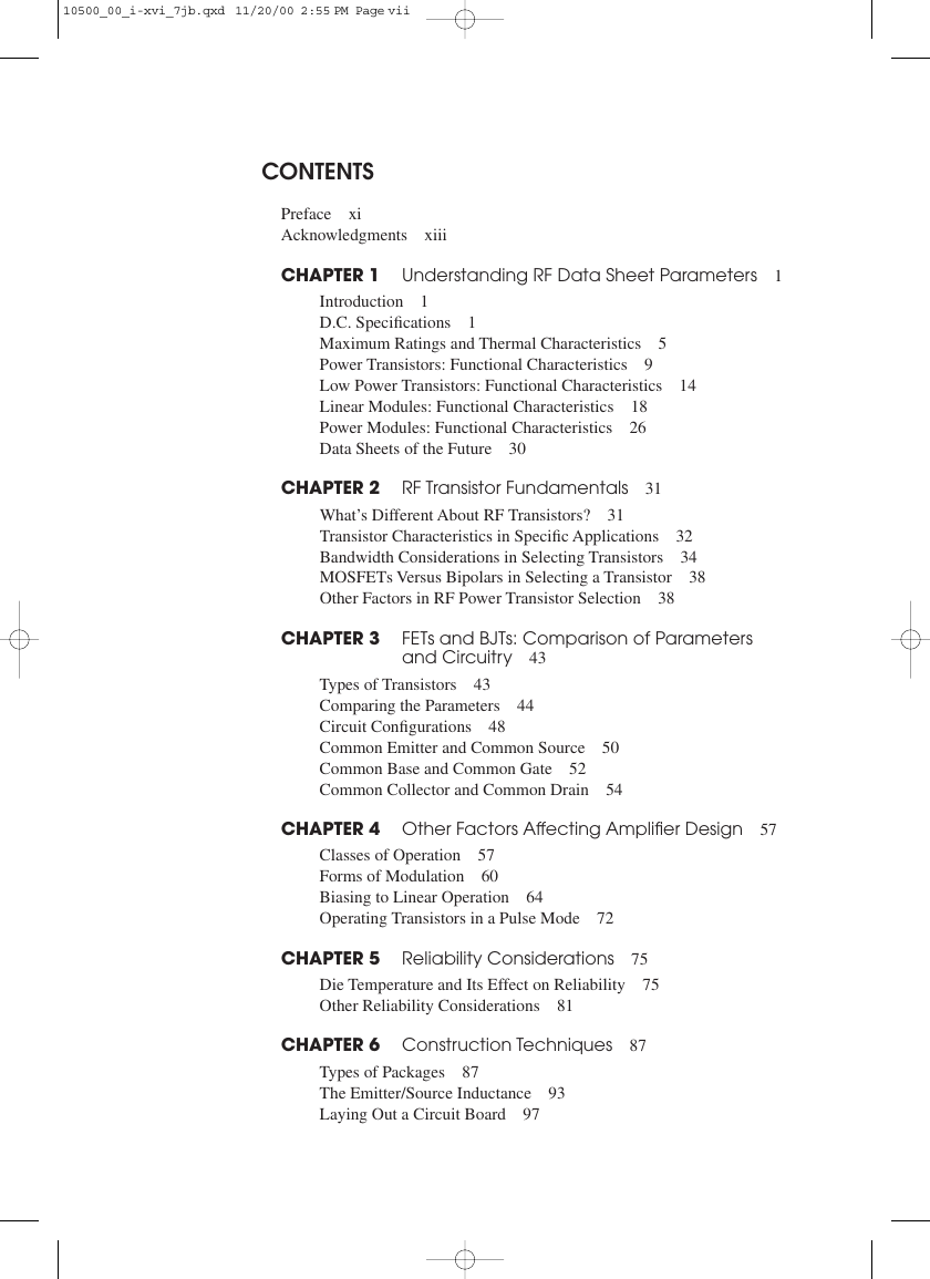
10500_00_i-xvi_7jb.qxd 11/20/00 2:55 PM Page vii CONTENTS Preface Acknowledgments xi xiii CHAPTER 1 Understanding RF Data Sheet Parameters 1 1 Introduction 1 D.C. Specifications Maximum Ratings and Thermal Characteristics Power Transistors: Functional Characteristics Low Power Transistors: Functional Characteristics 14 Linear Modules: Functional Characteristics Power Modules: Functional Characteristics Data Sheets of the Future 30 18 26 5 9 CHAPTER 2 RF Transistor Fundamentals 31 What’s Different About RF Transistors? Transistor Characteristics in Specific Applications 32 Bandwidth Considerations in Selecting Transistors 34 MOSFETs Versus Bipolars in Selecting a Transistor 38 Other Factors in RF Power Transistor Selection 31 38 CHAPTER 3 FETs and BJTs: Comparison of Parameters and Circuitry 43 Types of Transistors 43 Comparing the Parameters 44 Circuit Configurations Common Emitter and Common Source Common Base and Common Gate 52 Common Collector and Common Drain 48 50 54 CHAPTER 4 Other Factors Affecting Amplifier Design 57 Classes of Operation Forms of Modulation Biasing to Linear Operation Operating Transistors in a Pulse Mode 57 60 64 72 CHAPTER 5 Reliability Considerations 75 Die Temperature and Its Effect on Reliability Other Reliability Considerations 81 75 CHAPTER 6 Construction Techniques 87 Types of Packages The Emitter/Source Inductance 97 Laying Out a Circuit Board 87 93 1 2 3 4 5 6 7 8 9 10 11 12 13 14 15 16 17 18 19 20 21 22 23 24 25 26 27 28 29 30 31 32 33 34 35 36 37 38 39 40 41 42 43 44 45Short 46Reg
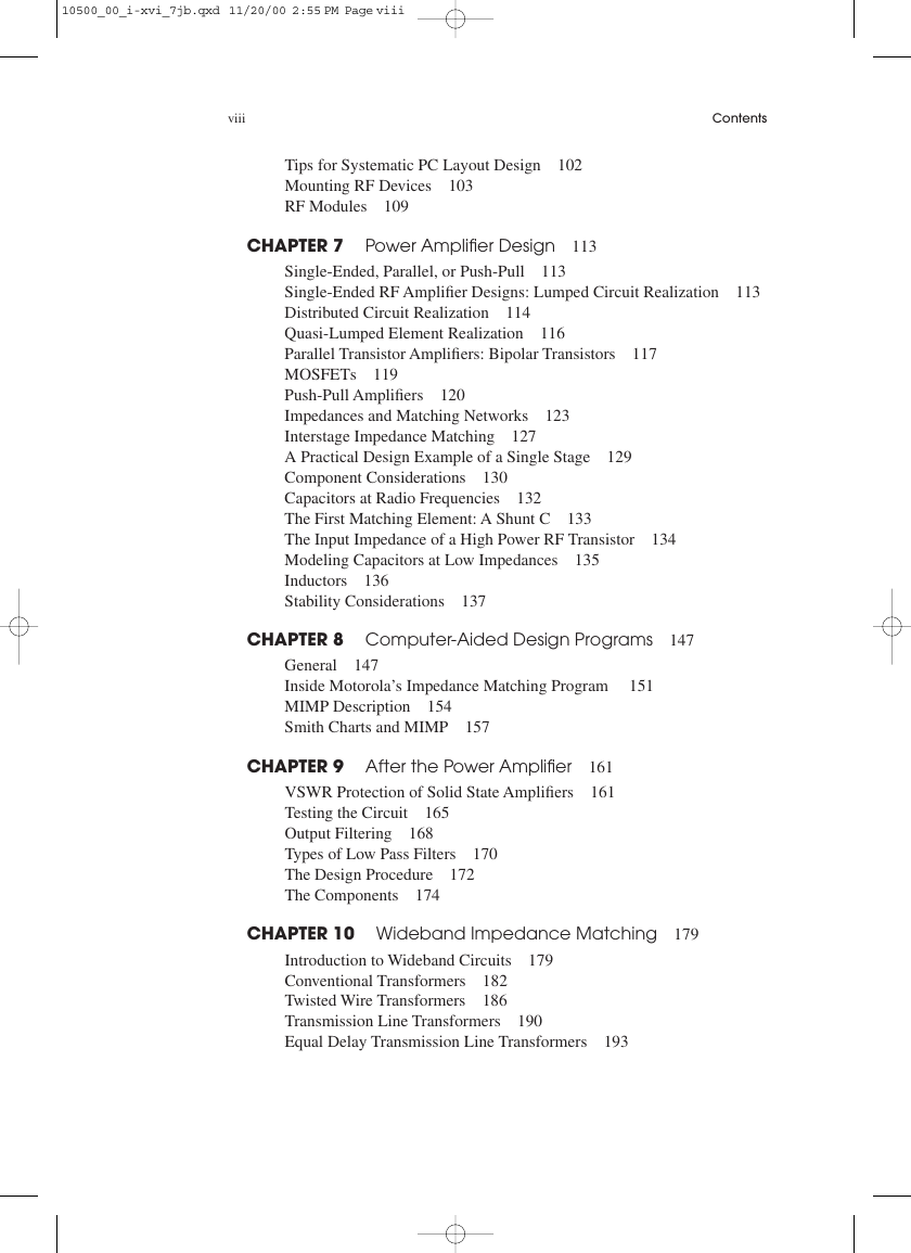
10500_00_i-xvi_7jb.qxd 11/20/00 2:55 PM Page viii viii Contents Tips for Systematic PC Layout Design Mounting RF Devices RF Modules 103 109 102 CHAPTER 7 Power Amplifier Design 113 113 116 127 119 113 Single-Ended, Parallel, or Push-Pull Single-Ended RF Amplifier Designs: Lumped Circuit Realization Distributed Circuit Realization 114 Quasi-Lumped Element Realization Parallel Transistor Amplifiers: Bipolar Transistors 117 MOSFETs Push-Pull Amplifiers 120 Impedances and Matching Networks 123 Interstage Impedance Matching A Practical Design Example of a Single Stage 129 Component Considerations 130 Capacitors at Radio Frequencies The First Matching Element: A Shunt C 133 The Input Impedance of a High Power RF Transistor 134 Modeling Capacitors at Low Impedances Inductors 136 Stability Considerations 135 132 137 CHAPTER 8 Computer-Aided Design Programs 147 147 General Inside Motorola’s Impedance Matching Program MIMP Description Smith Charts and MIMP 157 154 151 CHAPTER 9 After the Power Amplifier 161 VSWR Protection of Solid State Amplifiers 161 Testing the Circuit Output Filtering Types of Low Pass Filters 170 The Design Procedure 172 The Components 165 168 174 CHAPTER 10 Wideband Impedance Matching 179 179 Introduction to Wideband Circuits Conventional Transformers 182 Twisted Wire Transformers 186 Transmission Line Transformers 190 Equal Delay Transmission Line Transformers 193 1 2 3 4 5 6 7 8 9 10 11 12 13 14 15 16 17 18 19 20 21 22 23 24 25 26 27 28 29 30 31 32 33 34 35 36 37 38 39 40 41 42 43 44 Short45 Reg46
分享到:
收藏