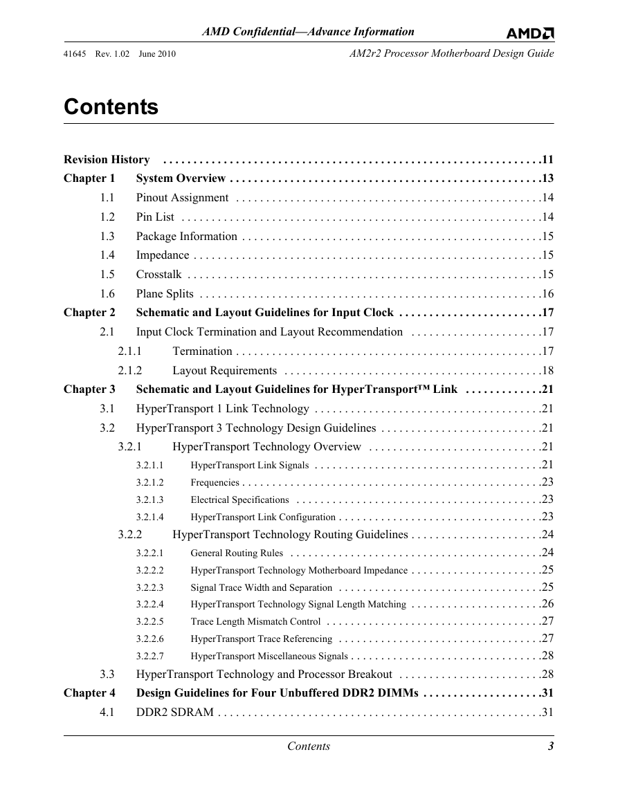
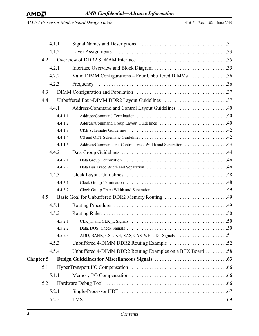
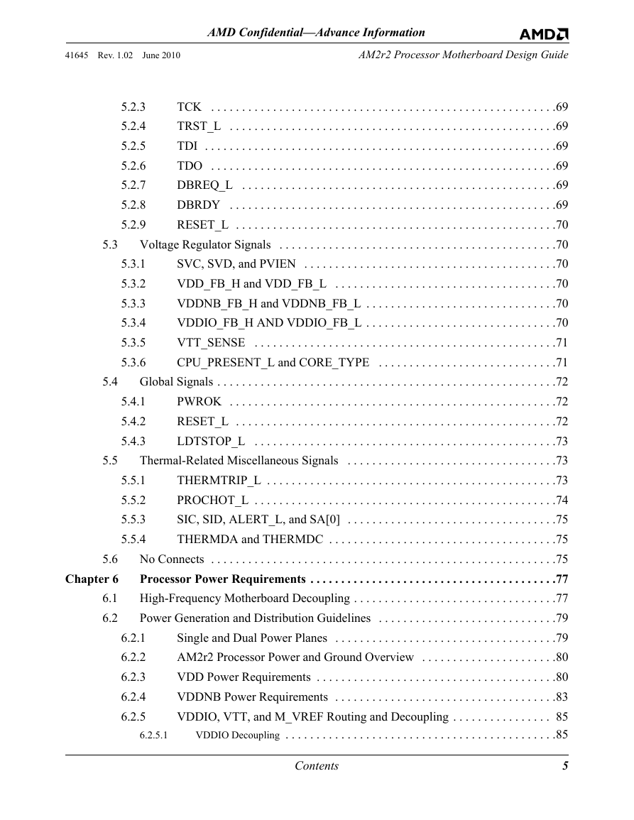
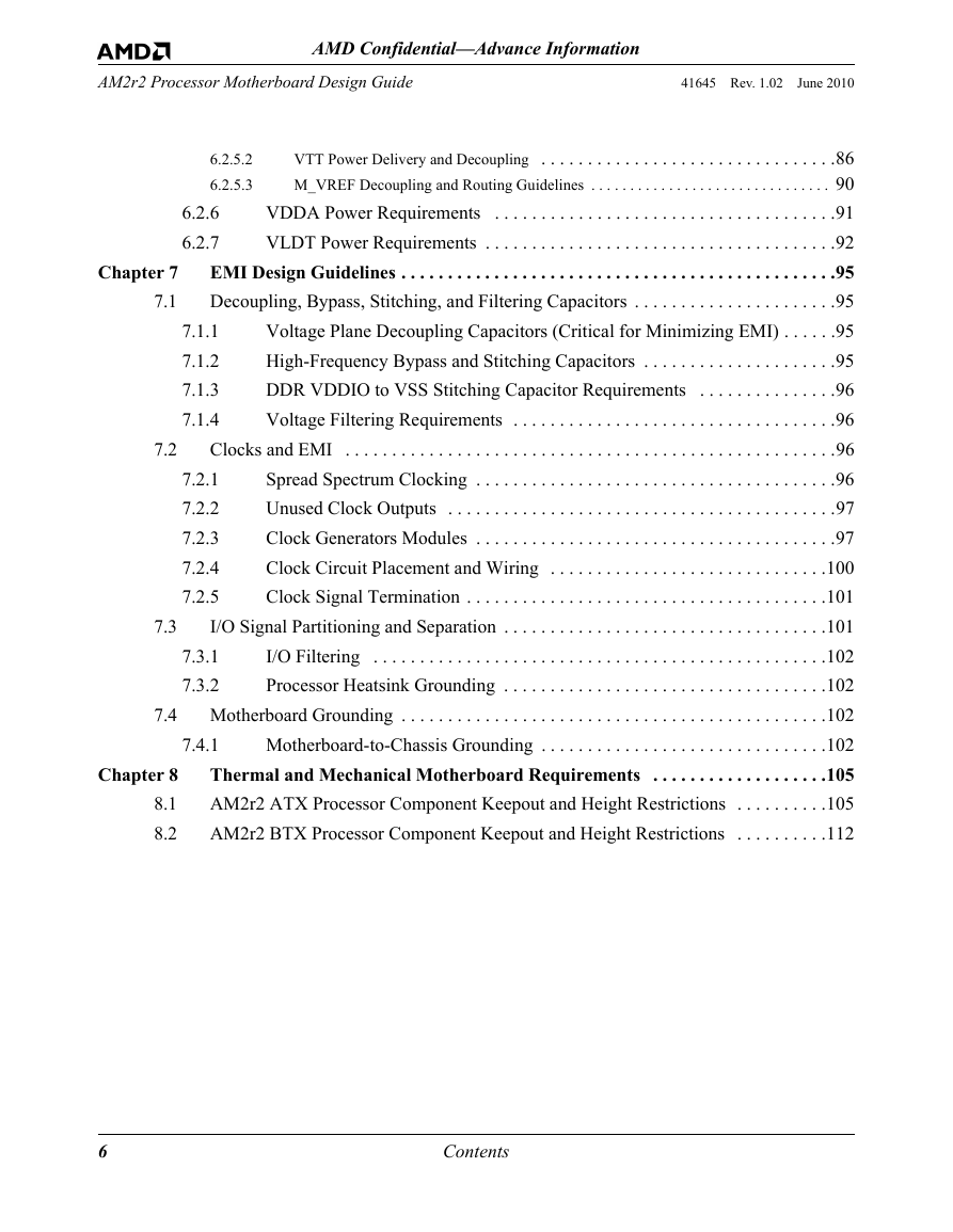
Contents
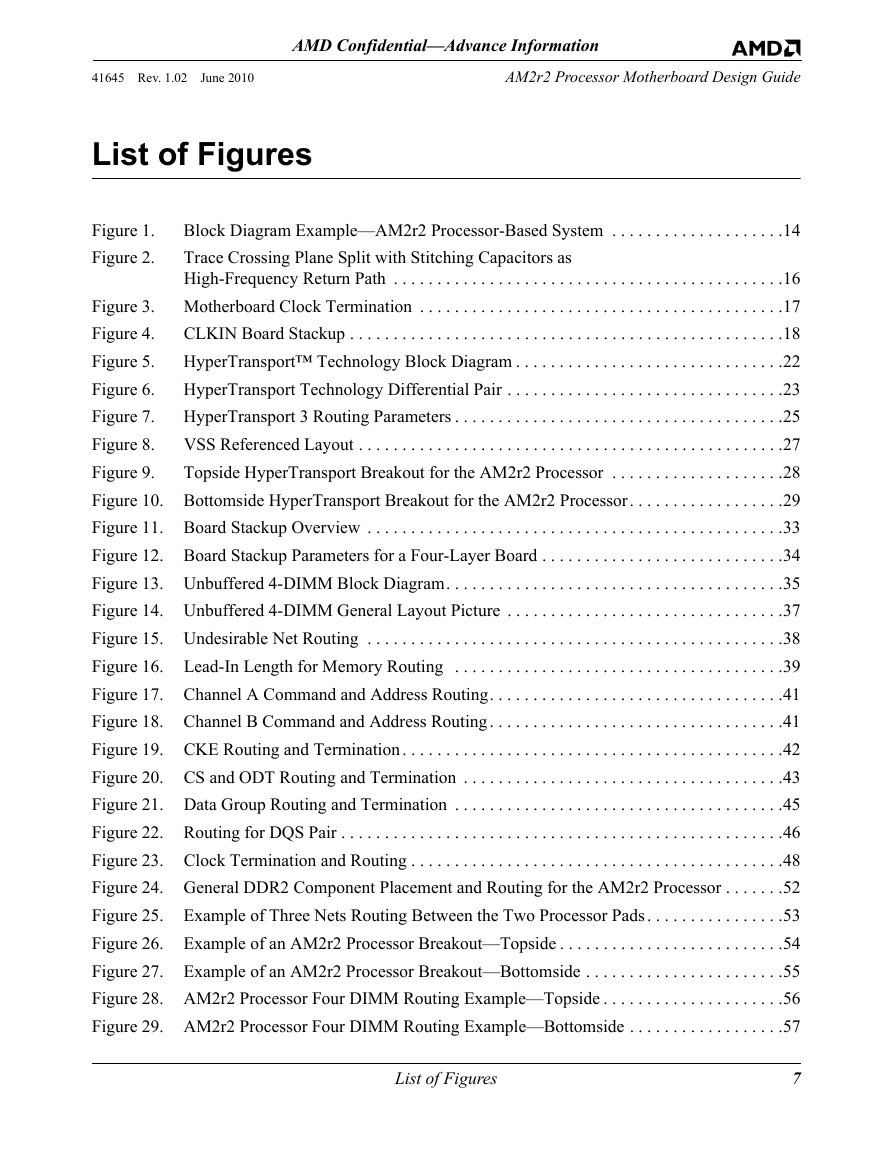
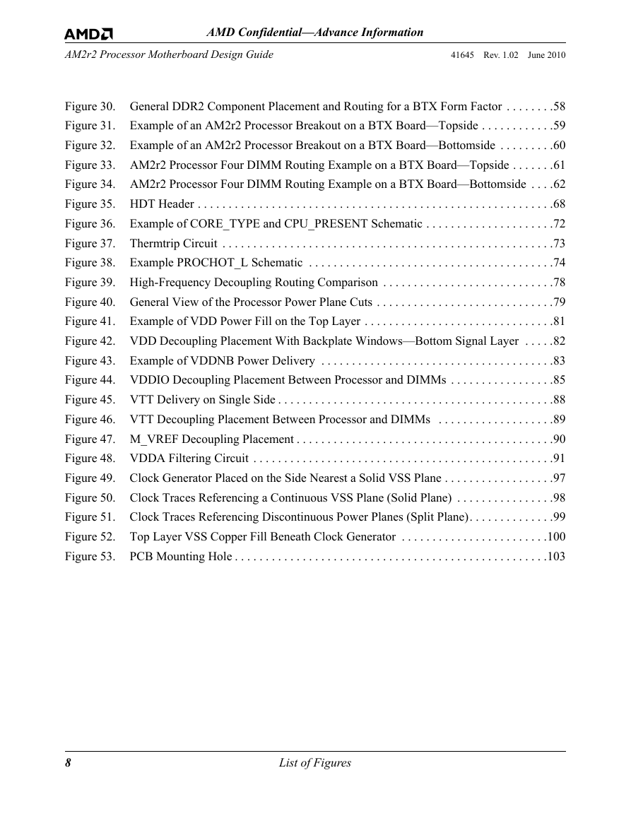
List of Figures
List of Tables
Chapter 1 System Overview
Table 1. Feature Compatibility
Figure 1. Block Diagram Example—AM2r2 Processor-Based System
1.1 Pinout Assignment
1.2 Pin List
1.3 Package Information
1.4 Impedance
1.5 Crosstalk
1.6 Plane Splits
Figure 2. Trace Crossing Plane Split with Stitching Capacitors as High-Frequency Return Path
Chapter 2 Schematic and Layout Guidelines for Input Clock
2.1 Input Clock Termination and Layout Recommendation
2.1.1 Termination
Figure 3. Motherboard Clock Termination
Table 2. Clock Termination Values
2.1.2 Layout Requirements
Figure 4. CLKIN Board Stackup
Table 3. CLKIN Board Routing Parameters
Chapter 3 Schematic and Layout Guidelines for HyperTransport™ Link
3.1 HyperTransport™ 1 Link Technology
3.2 HyperTransport™ 3 Technology Design Guidelines
3.2.1 HyperTransport™ Technology Overview
Figure 5. HyperTransport™ Technology Block Diagram
Figure 6. HyperTransport™ Technology Differential Pair
3.2.2 HyperTransport™ Technology Routing Guidelines
Table 4. Examples of Board Routing Parameters for 93-W Target Impedance (Measurements are in Mils)
Figure 7. HyperTransport™ 3 Routing Parameters
Table 5. Differential Pair Matching Rules
Table 6. Length-Matching Rules Within Each Clock Group
Table 7. CAD-to-CAD Length-Matching Rules Across Two Different Clock Groups
Figure 8. VSS Referenced Layout
3.3 HyperTransport™ Technology and Processor Breakout
Figure 9. Topside HyperTransport™ Breakout for the AM2r2 Processor
Figure 10. Bottomside HyperTransport™ Breakout for the AM2r2 Processor
Chapter 4 Design Guidelines for Four Unbuffered DDR2 DIMMs
4.1 DDR2 SDRAM
4.1.1 Signal Names and Descriptions
Table 8. DDR2 Signal Descriptions
Table 9. Clock Connections
4.1.2 Layer Assignments
Figure 11. Board Stackup Overview
Figure 12. Board Stackup Parameters for a Four-Layer Board
Table 10. Parameters for Stackup on a Four-Layer Board
4.2 Overview of DDR2 SDRAM Interface
4.2.1 Interface Overview and Block Diagram
Figure 13. Unbuffered 4-DIMM Block Diagram
4.2.2 Valid DIMM Configurations – Four Unbuffered DIMMs
4.2.3 Frequency
4.3 DIMM Configuration and Population
4.4 Unbuffered Four-DIMM DDR2 Layout Guidelines
Figure 14. Unbuffered 4-DIMM General Layout Picture
Figure 15. Undesirable Net Routing
Figure 16. Lead-In Length for Memory Routing
4.4.1 Address/Command and Control Layout Guidelines
Table 11. Termination Values for Unbuffered DIMM Address/Command Signals
Figure 17. Channel A Command and Address Routing
Figure 18. Channel B Command and Address Routing
Figure 19. CKE Routing and Termination
Figure 20. CS and ODT Routing and Termination
Table 12. Parameters for Address/Command and Control Trace Width and Space
4.4.2 Data Group Guidelines
Table 13. DDR2 Data Groups
Figure 21. Data Group Routing and Termination
Figure 22. Routing for DQS Pair
Table 14. Parameters for DQS Trace Width and Space
Table 15. Parameters for Data and Check Trace Width and Space
4.4.3 Clock Layout Guidelines
Figure 23. Clock Termination and Routing
Table 16. CLK_H and CLK_L Termination
Table 17. Parameters for CLK Trace Width and Space
4.5 Basic Goal for Unbuffered DDR2 Memory Routing
4.5.1 Routing Procedure
4.5.2 Routing Rules
4.5.3 Unbuffered 4-DIMM DDR2 Routing Example
Figure 24. General DDR2 Component Placement and Routing for the AM2r2 Processor
Figure 25. Example of Three Nets Routing Between the Two Processor Pads
Figure 26. Example of an AM2r2 Processor Breakout—Topside
Figure 27. Example of an AM2r2 Processor Breakout—Bottomside
Figure 28. AM2r2 Processor Four DIMM Routing Example—Topside
Figure 29. AM2r2 Processor Four DIMM Routing Example—Bottomside
4.5.4 Unbuffered 4-DIMM DDR2 Routing Examples on a BTX Board
Figure 30. General DDR2 Component Placement and Routing for a BTX Form Factor
Figure 31. Example of an AM2r2 Processor Breakout on a BTX Board—Topside
Figure 32. Example of an AM2r2 Processor Breakout on a BTX Board—Bottomside
Figure 33. AM2r2 Processor Four DIMM Routing Example on a BTX Board—Topside
Figure 34. AM2r2 Processor Four DIMM Routing Example on a BTX Board— Bottomside
Chapter 5 Design Guidelines for Miscellaneous Signals
Table 18. Miscellaneous Signals Quick Reference
5.1 HyperTransport™ I/O Compensation
Table 19. Compensation Resistor Routing Rules for HyperTransport™ Technology
5.1.1 Memory I/O Compensation
Table 20. Compensation Resistor Routing Rules for M_ZP and M_ZN
5.2 Hardware Debug Tool
5.2.1 Single-Processor HDT
Figure 35. HDT Header
Table 21. HDT Header Pin-Out
5.2.2 TMS
5.2.3 TCK
5.2.4 TRST_L
5.2.5 TDI
5.2.6 TDO
5.2.7 DBREQ_L
5.2.8 DBRDY
5.2.9 RESET_L
5.3 Voltage Regulator Signals
5.3.1 SVC, SVD, and PVIEN
5.3.2 VDD_FB_H and VDD_FB_L
5.3.3 VDDNB_FB_H and VDDNB_FB_L
5.3.4 VDDIO_FB_H AND VDDIO_FB_L
5.3.5 VTT_SENSE
5.3.6 CPU_PRESENT_L and CORE_TYPE
Figure 36. Example of CORE_TYPE and CPU_PRESENT Schematic
5.4 Global Signals
5.4.1 PWROK
5.4.2 RESET_L
5.4.3 LDTSTOP_L
5.5 Thermal-Related Miscellaneous Signals
5.5.1 THERMTRIP_L
Figure 37. Thermtrip Circuit
5.5.2 PROCHOT_L
Figure 38. Example PROCHOT_L Schematic
5.5.3 SIC, SID, ALERT_L, and SA[0]
5.5.4 THERMDA and THERMDC
5.6 No Connects
Chapter 6 Processor Power Requirements
6.1 High-Frequency Motherboard Decoupling
Figure 39. High-Frequency Decoupling Routing Comparison
6.2 Power Generation and Distribution Guidelines
Figure 40. General View of the Processor Power Plane Cuts
6.2.1 Single and Dual Power Planes
6.2.2 AM2r2 Processor Power and Ground Overview
6.2.3 VDD Power Requirements
Figure 41. Example of VDD Power Fill on the Top Layer
Table 22. VDD Decoupling Recommendations
Figure 42. VDD Decoupling Placement With Backplate Windows—Bottom Signal Layer
6.2.4 VDDNB Power Requirements
Figure 43. Example of VDDNB Power Delivery
Table 23. VDDNB Decoupling Recommendations
6.2.5 VDDIO, VTT, and M_VREF Routing and Decoupling
Figure 44. VDDIO Decoupling Placement Between Processor and DIMMs
Table 24. VDDIO Decoupling Recommendations
Table 25. VTT Decoupling Recommendations
Figure 45. VTT Delivery on Single Side
Figure 46. VTT Decoupling Placement Between Processor and DIMMs
Table 26. M_VREF-to-Processor Decoupling Recommendations
Figure 47. M_VREF Decoupling Placement
6.2.6 VDDA Power Requirements
Figure 48. VDDA Filtering Circuit
Table 27. VDDA Filter Recommendations
6.2.7 VLDT Power Requirements
Table 28. VLDT Decoupling Recommendations
Chapter 7 EMI Design Guidelines
7.1 Decoupling, Bypass, Stitching, and Filtering Capacitors
7.1.1 Voltage Plane Decoupling Capacitors (Critical for Minimizing EMI)
7.1.2 High-Frequency Bypass and Stitching Capacitors
7.1.3 DDR VDDIO to VSS Stitching Capacitor Requirements
7.1.4 Voltage Filtering Requirements
7.2 Clocks and EMI
7.2.1 Spread Spectrum Clocking
7.2.2 Unused Clock Outputs
7.2.3 Clock Generator Modules
Figure 49. Clock Generator Placed on the Side Nearest a Solid VSS Plane
Figure 50. Clock Traces Referencing a Continuous VSS Plane (Solid Plane)
Figure 51. Clock Traces Referencing Discontinuous Power Planes (Split Plane)
Figure 52. Top Layer VSS Copper Fill Beneath Clock Generator
7.2.4 Clock Circuit Placement and Wiring
7.2.5 Clock Signal Termination
7.3 I/O Signal Partitioning and Separation
7.3.1 I/O Filtering
7.3.2 Processor Heatsink Grounding
7.4 Motherboard Grounding
7.4.1 Motherboard-to-Chassis Grounding
Figure 53. PCB Mounting Hole
Chapter 8 Thermal and Mechanical Motherboard Requirements
8.1 AM2r2 ATX Processor Component Keepout and Height Restrictions
8.2 AM2r2 BTX Processor Component Keepout and Height Restrictions



 2023年江西萍乡中考道德与法治真题及答案.doc
 2012年重庆南川中考生物真题及答案.doc
 2013年江西师范大学地理学综合及文艺理论基础考研真题.doc
 2020年四川甘孜小升初语文真题及答案I卷.doc
 2020年注册岩土工程师专业基础考试真题及答案.doc
 2023-2024学年福建省厦门市九年级上学期数学月考试题及答案.doc
 2021-2022学年辽宁省沈阳市大东区九年级上学期语文期末试题及答案.doc
 2022-2023学年北京东城区初三第一学期物理期末试卷及答案.doc
 2018上半年江西教师资格初中地理学科知识与教学能力真题及答案.doc
 2012年河北国家公务员申论考试真题及答案-省级.doc
 2020-2021学年江苏省扬州市江都区邵樊片九年级上学期数学第一次质量检测试题及答案.doc
 2022下半年黑龙江教师资格证中学综合素质真题及答案.doc