Titl
®
CPS-1848™ Datasheet
Central Packet Switch
Preliminary Status
February 2, 2011
6024 Silver Creek Valley Road, San Jose, California 95138
Telephone: (408) 284-8200 • Fax: (408) 284-3572
©2011 Integrated Device Technology, Inc.
�
GENERAL DISCLAIMER
Integrated Device Technology, Inc. (“IDT”) reserves the right to make changes to its products or specifications at any time, without notice,
in order to improve design or performance. IDT does not assume responsibility for use of any circuitry described herein other than the
circuitry embodied in an IDT product. Disclosure of the information herein does not convey a license or any other right, by implication or
otherwise, in any patent, trademark, or other intellectual property right of IDT. IDT products may contain errata which can affect product
performance to a minor or immaterial degree. Current characterized errata will be made available upon request. Items identified herein as
“reserved” or “undefined” are reserved for future definition. IDT does not assume responsibility for conflicts or incompatibilities arising
from the future definition of such items. IDT products have not been designed, tested, or manufactured for use in, and thus are not
warranted for, applications where the failure, malfunction, or any inaccuracy in the application carries a risk of death, serious bodily injury,
or damage to tangible property. Code examples provided herein by IDT are for illustrative purposes only and should not be relied upon for
developing applications. Any use of such code examples shall be at the user's sole risk.
Copyright ©2011 Integrated Device Technology, Inc.
The IDT logo is registered to Integrated Device Technology, Inc.
“Accelerated Thinking” is a service mark of Integrated Device Technology, Inc.
�
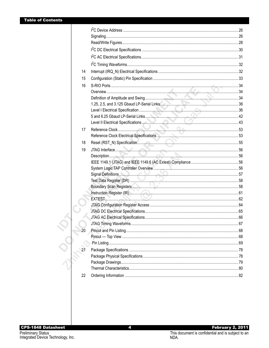
Table of Contents
Table of Contents
Introduction ...........................................................................................................................................5
Additional Resources ............................................................................................................................5
Document Conventions and Definitions................................................................................................5
Revision History ....................................................................................................................................5
Device Overview..........................................................................................................................7
1
2
Features ......................................................................................................................................7
Block Diagram .............................................................................................................................9
3
Device Description.......................................................................................................................9
4
5
Functional Overview..................................................................................................................10
Interface Overview..................................................................................................................... 11
6
S-RIO Ports ............................................................................................................................... 11
I2C Bus...................................................................................................................................... 11
JTAG TAP Port .......................................................................................................................... 11
Interrupt (IRQ_N)....................................................................................................................... 11
Reset (RST_N).......................................................................................................................... 11
Clock (REF_CLK_P/N)..............................................................................................................12
Rext (REXT_N/P) ......................................................................................................................12
Speed Select (SPD[2:0]) ...........................................................................................................12
Quadrant Config (QCFG[7:0]) ...................................................................................................12
Frequency Select (FSEL[1:0]) ...................................................................................................12
Multicast (MCAST) ....................................................................................................................12
Configuration Pins .....................................................................................................................13
Speed Select Pins SPD[2:0]......................................................................................................13
Quadrant Configuration Pins QCFG[7:0]...................................................................................13
Absolute Maximum Ratings.......................................................................................................16
8
Recommended Operating Conditions .......................................................................................17
9
10 AC Test Conditions....................................................................................................................18
11 Device Performance Data .........................................................................................................20
Performance Figures.................................................................................................................20
Sustained Per-Port Throughput (Typical) ..................................................................................21
Data Packet Latency in “Cut-Through” Mode (Typical)..............................................................22
Maintenance Packet Latency (Typical)......................................................................................22
Doorbell Packet Latency (Typical).............................................................................................23
Multicast-Event Control Symbol Latency (Typical) ....................................................................23
12 Power Figures ...........................................................................................................................24
Typical Power ............................................................................................................................24
Maximum Power........................................................................................................................25
I2C Bus ......................................................................................................................................26
I2C Master Mode and Slave Mode ............................................................................................26
13
7
CPS-1848 Datasheet
Preliminary Status
Integrated Device Technology, Inc.
3
February 2, 2011
This document is confidential and is subject to an
NDA.
�
Table of Contents
I2C Device Address ...................................................................................................................26
Signaling....................................................................................................................................26
Read/Write Figures....................................................................................................................28
I2C DC Electrical Specifications ................................................................................................30
I2C AC Electrical Specifications.................................................................................................31
I2C Timing Waveforms...............................................................................................................32
14
Interrupt (IRQ_N) Electrical Specifications................................................................................32
15 Configuration (Static) Pin Specification .....................................................................................33
16 S-RIO Ports ...............................................................................................................................34
Overview....................................................................................................................................34
Definition of Amplitude and Swing.............................................................................................34
1.25, 2.5, and 3.125 Gbaud LP-Serial Links..............................................................................36
Level I Electrical Specification...................................................................................................36
5 and 6.25 Gbaud LP-Serial Links.............................................................................................42
Level II Electrical Specifications ................................................................................................43
17 Reference Clock........................................................................................................................53
Reference Clock Electrical Specifications .................................................................................53
18 Reset (RST_N) Specification.....................................................................................................55
JTAG Interface...........................................................................................................................56
19
Description.................................................................................................................................56
IEEE 1149.1 (JTAG) and IEEE 1149.6 (AC Extest) Compliance...............................................56
System Logic TAP Controller Overview.....................................................................................56
Signal Definitions.......................................................................................................................57
Test Data Register (DR) ............................................................................................................58
Boundary Scan Registers..........................................................................................................58
Instruction Register (IR).............................................................................................................61
EXTEST.....................................................................................................................................62
JTAG Configuration Register Access ........................................................................................64
JTAG DC Electrical Specifications.............................................................................................65
JTAG AC Electrical Specifications.............................................................................................66
JTAG Timing Waveforms...........................................................................................................67
20 Pinout and Pin Listing................................................................................................................68
Pinout — Top View ....................................................................................................................68
Pin Listing.................................................................................................................................69
21 Package Specifications .............................................................................................................78
Package Physical Specifications...............................................................................................78
Package Drawings.....................................................................................................................79
Thermal Characteristics.............................................................................................................80
22 Ordering Information .................................................................................................................82
CPS-1848 Datasheet
Preliminary Status
Integrated Device Technology, Inc.
4
February 2, 2011
This document is confidential and is subject to an
NDA.
�
About This Document
Introduction
The CPS-1848 Datasheet provides hardware information about the CPS-1848, such as electrical and
packaging characteristics. It is intended for hardware engineers who are designing system interconnect
applications with the device.
Additional Resources
The CPS-1848 User Manual describes the functionality and configuration capabilities of the device. In
addition, there are many other resources available that support the CPS-1848. For more information,
please contact IDT for support.
Document Conventions and Definitions
This document uses the following conventions and definitions:
•
To indicate signal states:
– Differential signals use the suffix “_P” to indicate the positive half of a differential pair.
– Differential signals use the suffix “_N” to indicate the negative half of a differential pair.
– Non-differential signals use the suffix “_N” to indicate an active-low state.
To define buses, the most significant bit (MSB) is on the left and least significant bit (LSB) is on the right.
No leading zeros are included.
To represent numerical values, either decimal, binary, or hexadecimal formats are used. The binary
format is as follows: 0bDDD, where “D” represents either 0 or 1; the hexadecimal format is as follows:
0xDD, where “D” represents the hexadecimal digit(s); otherwise, it is decimal.
•
•
• Unless otherwise denoted, a byte refers to an 8-bit quantity; a word refers to a 32-bit quantity, and a
double word refers to an 8-byte (64-bit) quantity. This is in accordance with RapidIO convention.
• A bit is set when its value is 0b1. A bit is cleared when its value is 0b0.
• A read-only register, bit, or field is one that can be read but not modified.
This symbol indicates important configuration information or suggestions.
This symbol indicates procedures or operating levels that may result in misuse or damage to the
device.
Revision History
•
February 2, 2011, Preliminary Datasheet
– Updated Maximum Power Consumption Numbers
– Fixed a number of minor errors
• December 21, 2010, Preliminary Datasheet
– Updated Power Consumption Numbers
– Added Configuration (Static) Pin Specification section
– Updated Package Drawings diagram
CPS-1848 Datasheet
Preliminary Status
Integrated Device Technology, Inc.
5
February 2, 2011
This document is confidential and is subject to an
NDA.
�
About This Document
– Added Thermal Characteristics section
• October 5, 2010, Preliminary Datasheet
– Added couple of usage notes below the JTAG Pin Description table
– Included 2.5V power supply to the I2C DC Electrical Specification section
• September 3, 2010, Preliminary Datasheet
•
•
– Added Reset section and associated timing diagram
– Added Theta JB parameter in Package Specification section
– Added JTAG device chaining restriction in the JTAG section
June 28, 2010, Preliminary Datasheet
– Updated thermal data in Package Specification section
– Added new package option HM in the Ordering Infomation section
June 21, 2010, Preliminary Datasheet
– Added new Package Drawings
– Changed the signal formatting consistency of the following signals: FSEL[1:0], ID[9:0], SPD[2:0], and
QCFG[7:0]. No pinout changes were made
• April 26, 2010, Preliminary Datasheet
– Added differential signal indicator in S-RIO Lanes Test Load notes section
– Removed Usage Consideration contents in the JTAG section, not applicable
– Updated the JTAG deviceID in the IDCODE section
– Updated the FSEL1 pin definition in the Pin Listing section
• March 15, 2010, Preliminary Datasheet
– Added recommended AC-coupling capacitor values for S-RIO Lanes Test Load
– Added absolute maximum ratings values for VDD, VDDT, VDDA and VDDS rails
– Removed I/O terminal voltage for the following; VDD, VDDT, VDDA and VDDS, not applicable
– Updated note 1 under the Recommended Operating Conditions section
– Added a note regarding automatic swapping of differential signal pair and automatic reordering of
lanes to the Serial RapidIO Ports Overview section and Note section of the pin list table
– Updated MCAST pin description in the pin listing
– Updated the JTAG AC Electrical Specification
– Removed Supply Voltage and Ground requirements from JTAG DC Electrical specification
• December 14, 2009, Preliminary Datasheet
– Added more information about lane to port mapping in Quadrant Configuration Pins QCFG[7:0]
– Updated Absolute Maximum Ratings and Recommended Operating Conditions
– Changed the signal state indicators for all signals (see Document Conventions and Definitions)
• November 23, 2009, Preliminary Datasheet
– Added Reset to RapidIO link initialization specifications
– Updated all read/write protocol diagrams in I2C Bus
– Added additional configuration information about lanes, ports, quads, and quadrants in Quadrant
Configuration Pins QCFG[7:0]
– Revised document’s format and completed various editorial updates
• September 15, 2009, Advanced Datasheet. Initial release
CPS-1848 Datasheet
Preliminary Status
Integrated Device Technology, Inc.
6
February 2, 2011
This document is confidential and is subject to an
NDA.
�
CPS-1848 Datasheet
1 Device Overview
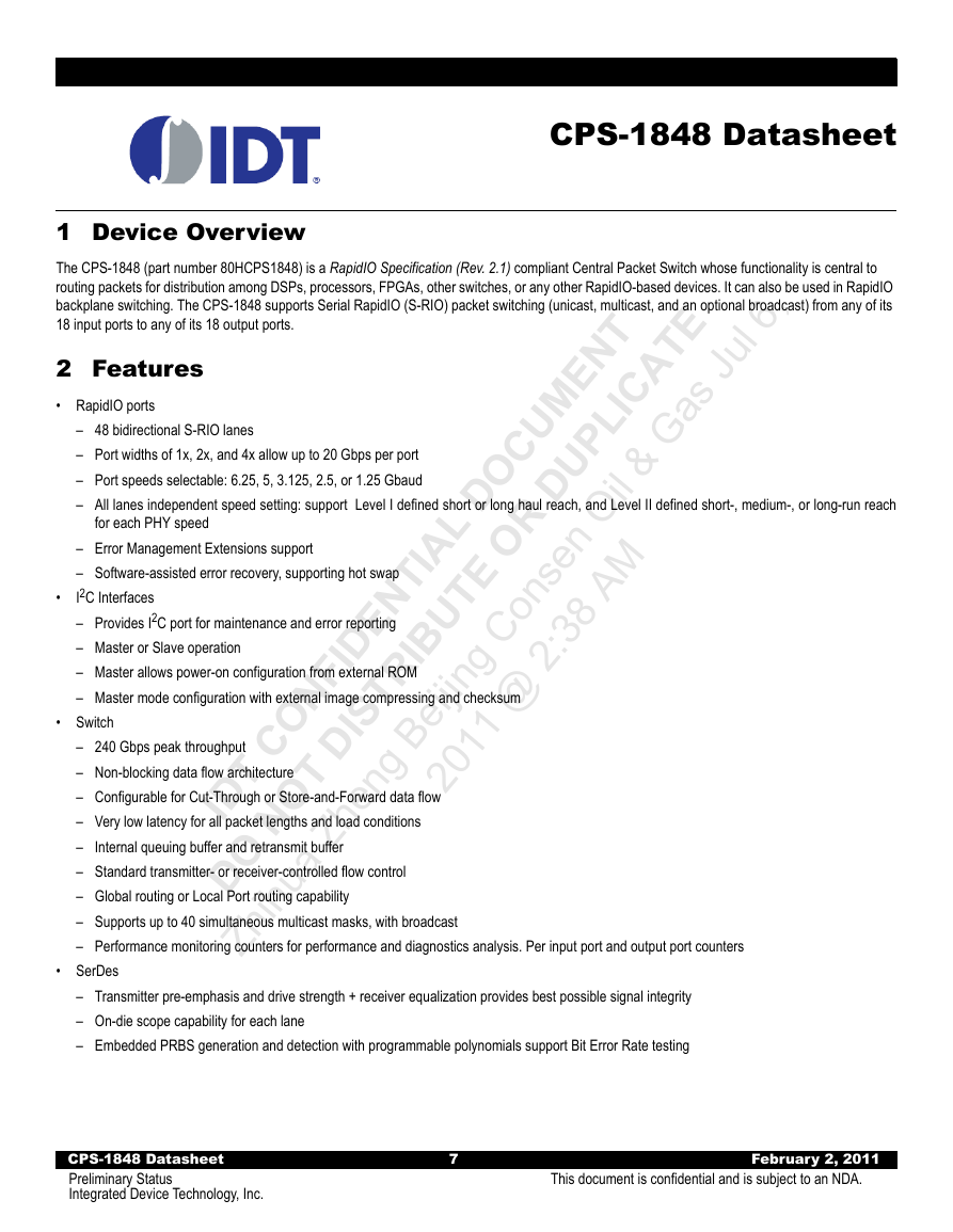
The CPS-1848 (part number 80HCPS1848) is a RapidIO Specification (Rev. 2.1) compliant Central Packet Switch whose functionality is central to
routing packets for distribution among DSPs, processors, FPGAs, other switches, or any other RapidIO-based devices. It can also be used in RapidIO
backplane switching. The CPS-1848 supports Serial RapidIO (S-RIO) packet switching (unicast, multicast, and an optional broadcast) from any of its
18 input ports to any of its 18 output ports.
2 Features
• RapidIO ports
– 48 bidirectional S-RIO lanes
– Port widths of 1x, 2x, and 4x allow up to 20 Gbps per port
– Port speeds selectable: 6.25, 5, 3.125, 2.5, or 1.25 Gbaud
– All lanes independent speed setting: support Level I defined short or long haul reach, and Level II defined short-, medium-, or long-run reach
for each PHY speed
•
– Error Management Extensions support
– Software-assisted error recovery, supporting hot swap
I2C Interfaces
– Provides I2C port for maintenance and error reporting
– Master or Slave operation
– Master allows power-on configuration from external ROM
– Master mode configuration with external image compressing and checksum
• Switch
– 240 Gbps peak throughput
– Non-blocking data flow architecture
– Configurable for Cut-Through or Store-and-Forward data flow
– Very low latency for all packet lengths and load conditions
– Internal queuing buffer and retransmit buffer
– Standard transmitter- or receiver-controlled flow control
– Global routing or Local Port routing capability
– Supports up to 40 simultaneous multicast masks, with broadcast
– Performance monitoring counters for performance and diagnostics analysis. Per input port and output port counters
• SerDes
– Transmitter pre-emphasis and drive strength + receiver equalization provides best possible signal integrity
– On-die scope capability for each lane
– Embedded PRBS generation and detection with programmable polynomials support Bit Error Rate testing
CPS-1848 Datasheet
Preliminary Status
Integrated Device Technology, Inc.
7
This document is confidential and is subject to an NDA.
February 2, 2011
�
2 Features
• Additional Information
– Packet Trace/Mirror. Each input port can copy all incoming packets matching user-defined criteria to a “trace” output port.
– Packet Filter. Each input port can filter (drop) all incoming packets matching user-defined criteria.
– Device configurable through any of S-RIO ports, I2C, or JTAG
– Full JTAG Boundary Scan Support (IEEE1149.1 and 1149.6)
– Lidless FCBGA Package: 29 X 29 mm, 1.0 mm ball pitch
• Specification Compliancy
– RapidIO Specification (Rev. 2.1), Part 1: Input/Output Logical Specification, 08/2009, RTA
– RapidIO Specification (Rev. 2.1), Part 2: Message Passing Logical Specification, 08/2009, RTA
– RapidIO Specification (Rev. 2.1), Part 3: Common Transport Specification, 08/2009, RTA
– RapidIO Specification (Rev. 2.1), Part 6: LP-Serial Physical Layer Specification, 08/2009, RTA
– RapidIO Specification (Rev. 2.1), Part 7: System and Device Interoperability Specification, 08/2009, RTA
– RapidIO Specification (Rev. 2.1), Part 8: Error Management Extensions Specification, 08/2009, RTA
– RapidIO Specification (Rev. 2.1), Part 9: Flow Control Logic Layer Extensions Specification, 08/2009, RTA
– RapidIO Specification (Rev. 2.1), Part 11: Multicast Extensions Specification, 08/2009, RTA
– RapidIO Specification (Rev. 2.1), Annex I: Software/System Bring Up Specification, 08/2009, RTA
– IEEE Std 1149.1-2001 IEEE Standard Test Access Port and Boundary-Scan Architecture
– IEEE Std 1149.6-2003 IEEE Standard for Boundary-Scan Testing of Advanced Digital Networks
– The I2C-BUS Specification (v 2.1), January 2000, Philips
CPS-1848 Datasheet
Preliminary Status
Integrated Device Technology, Inc.
8
This document is confidential and is subject to an NDA.
February 2, 2011
�




 2023年江西萍乡中考道德与法治真题及答案.doc
 2012年重庆南川中考生物真题及答案.doc
 2013年江西师范大学地理学综合及文艺理论基础考研真题.doc
 2020年四川甘孜小升初语文真题及答案I卷.doc
 2020年注册岩土工程师专业基础考试真题及答案.doc
 2023-2024学年福建省厦门市九年级上学期数学月考试题及答案.doc
 2021-2022学年辽宁省沈阳市大东区九年级上学期语文期末试题及答案.doc
 2022-2023学年北京东城区初三第一学期物理期末试卷及答案.doc
 2018上半年江西教师资格初中地理学科知识与教学能力真题及答案.doc
 2012年河北国家公务员申论考试真题及答案-省级.doc
 2020-2021学年江苏省扬州市江都区邵樊片九年级上学期数学第一次质量检测试题及答案.doc
 2022下半年黑龙江教师资格证中学综合素质真题及答案.doc