SPI(x1/x2/x4 I/O) NAND Flash 1Gb/2Gb
GD5F1GQ4XC
GD5F2GQ4XC
DATASHEET
1
GD Confidential Preliminary�
SPI(x1/x2/x4 I/O) NAND Flash 1Gb/2Gb
SPI (Serial Peripheral Interface) NAND Flash Memory
Product List
Vcc Range
1.7V ~ 2.0V
Page Size
Part No.
GD5F1GQ4RCYIXX
GD5F1GQ4RCFIXX
GD5F2GQ4RCYIXX
GD5F2GQ4RCFIXX
GD5F1GQ4UCYIXX
GD5F1GQ4UCFIXX
GD5F2GQ4UCYIXX
GD5F2GQ4UCFIXX
2.7V ~ 3.6V
2KByte + 128Byte
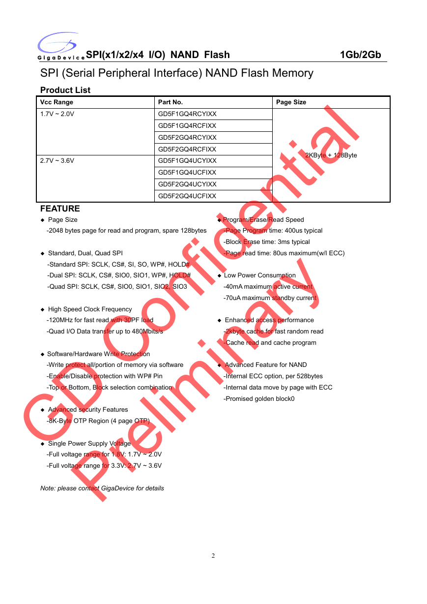
FEATURE
◆ Page Size
-2048 bytes page for read and program, spare 128bytes
◆ Standard, Dual, Quad SPI
-Standard SPI: SCLK, CS#, SI, SO, WP#, HOLD#
-Dual SPI: SCLK, CS#, SIO0, SIO1, WP#, HOLD#
-Quad SPI: SCLK, CS#, SIO0, SIO1, SIO2, SIO3
◆ High Speed Clock Frequency
-120MHz for fast read with 30PF load
-Quad I/O Data transfer up to 480Mbits/s
◆ Software/Hardware Write Protection
-Write protect all/portion of memory via software
-Enable/Disable protection with WP# Pin
-Top or Bottom, Block selection combination
◆ Advanced security Features
-8K-Byte OTP Region (4 page OTP)
◆ Single Power Supply Voltage
-Full voltage range for 1.8V: 1.7V ~ 2.0V
-Full voltage range for 3.3V: 2.7V ~ 3.6V
Note: please contact GigaDevice for details
◆ Program/Erase/Read Speed
-Page Program time: 400us typical
-Block Erase time: 3ms typical
-Page read time: 80us maximum(w/I ECC)
◆ Low Power Consumption
-40mA maximum active current
-70uA maximum standby current
◆ Enhanced access performance
-2kbyte cache for fast random read
-Cache read and cache program
◆ Advanced Feature for NAND
-Internal ECC option, per 528bytes
-Internal data move by page with ECC
-Promised golden block0
2
GD Confidential Preliminary�
GENERAL DESCRIPTION
SPI(x1/x2/x4 I/O) NAND Flash 1Gb/2Gb
SPI (Serial Peripheral Interface) NAND Flash provides an ultra cost-effective while high density non-volatile memory
storage solution for embedded systems, based on an industry-standard NAND Flash memory core. It is an attractive
alternative to SPI-NOR and standard parallel NAND Flash, with advanced features:
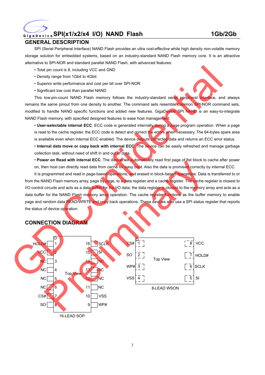
• Total pin count is 8, including VCC and GND
• Density range from 1Gbit to 4Gbit
• Superior write performance and cost per bit over SPI-NOR
• Significant low cost than parallel NAND
This low-pin-count NAND Flash memory follows the industry-standard serial peripheral interface, and always
remains the same pinout from one density to another. The command sets resemble common SPI-NOR command sets,
modified to handle NAND specific functions and added new features. GigaDevice SPI NAND is an easy-to-integrate
NAND Flash memory, with specified designed features to ease host management:
• User-selectable internal ECC. ECC code is generated internally during a page program operation. When a page
is read to the cache register, the ECC code is detect and correct the errors when necessary. The 64-bytes spare area
is available even when internal ECC enabled. The device outputs corrected data and returns an ECC error status.
• Internal data move or copy back with internal ECC. The device can be easily refreshed and manage garbage
collection task, without need of shift in and out of data.
• Power on Read with internal ECC. The device will automatically read first page of fist block to cache after power
on, then host can directly read data from cache for easy boot. Also the data is promised correctly by internal ECC.
It is programmed and read in page-based operations, and erased in block-based operations. Data is transferred to or
from the NAND Flash memory array, page by page, to a data register and a cache register. The cache register is closest to
I/O control circuits and acts as a data buffer for the I/O data; the data register is closest to the memory array and acts as a
data buffer for the NAND Flash memory array operation. The cache register functions as the buffer memory to enable
page and random data READ/WRITE and copy back operations. These devices also use a SPI status register that reports
the status of device operation.
CONNECTION DIAGRAM
CS#
SO
1
2
WP#
3
VSS
4
Top View
8–LEAD WSON
8
7
VCC
HOLD#
6
SCLK
5
SI
HOLD#
VCC
NC
NC
NC
NC
CS#
SO
1
2
3
4
5
6
7
8
Top View
16
15
14
13
12
11
10
9
SCLK
SI
NC
NC
NC
NC
VSS
WP#
16-LEAD SOP
3
GD Confidential Preliminary�
SPI(x1/x2/x4 I/O) NAND Flash 1Gb/2Gb
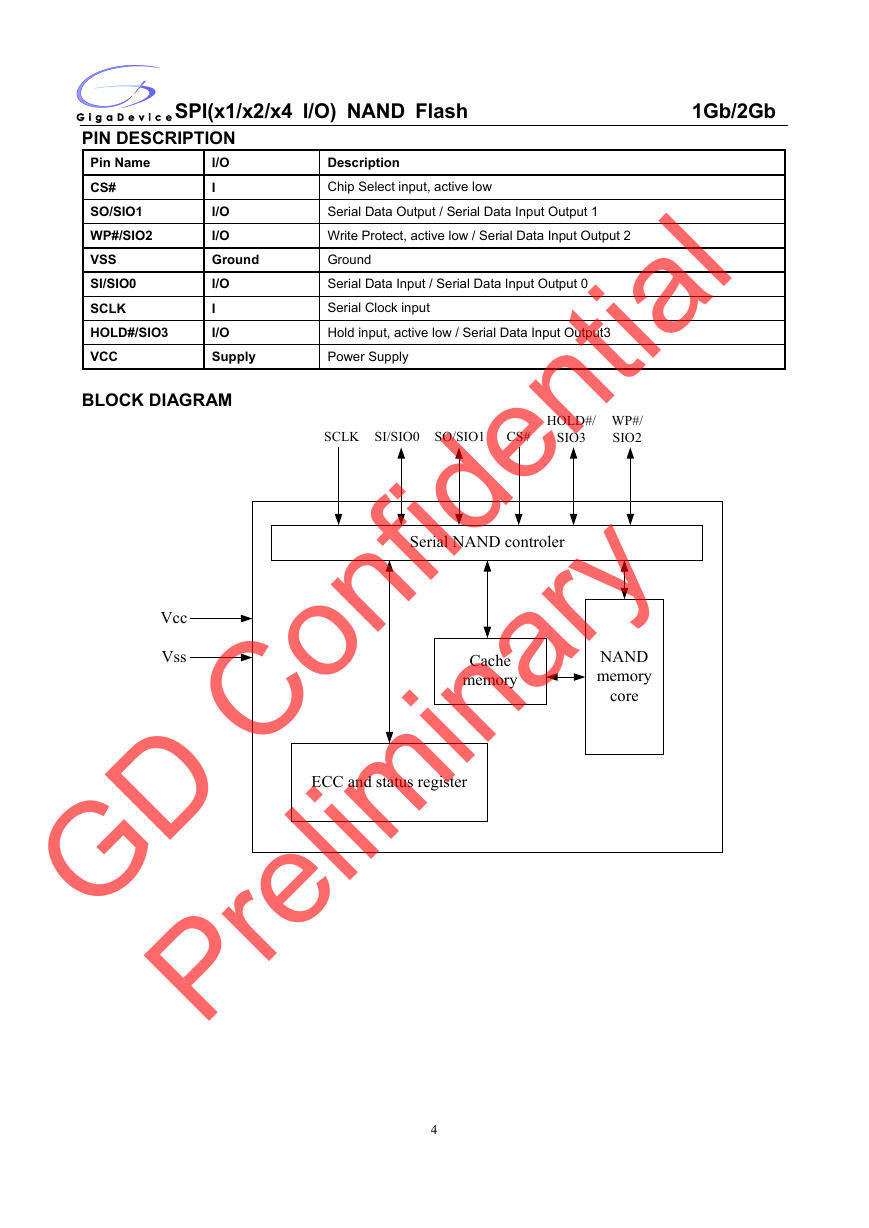
PIN DESCRIPTION
I/O
Pin Name
CS#
I
I/O
SO/SIO1
I/O
WP#/SIO2
VSS
Ground
I/O
SI/SIO0
I
SCLK
HOLD#/SIO3
I/O
Supply
VCC
BLOCK DIAGRAM
Vcc
Vss
Description
Chip Select input, active low
Serial Data Output / Serial Data Input Output 1
Write Protect, active low / Serial Data Input Output 2
Ground
Serial Data Input / Serial Data Input Output 0
Serial Clock input
Hold input, active low / Serial Data Input Output3
Power Supply
SCLK SI/SIO0 SO/SIO1
CS#
HOLD#/
SIO3
WP#/
SIO2
Serial NAND controler
Cache
memory
NAND
memory
core
ECC and status register
4
GD Confidential Preliminary�
SPI(x1/x2/x4 I/O) NAND Flash 1Gb/2Gb
ARRAY ORGANIZATION
Each device has
1G
128M+8M
1024 x 64
1024
2G
256M+16M
2048 x 64
2048
Each block has
Each page has
128K+8K
2K+128
64
-
-
-
bytes
pages
blocks
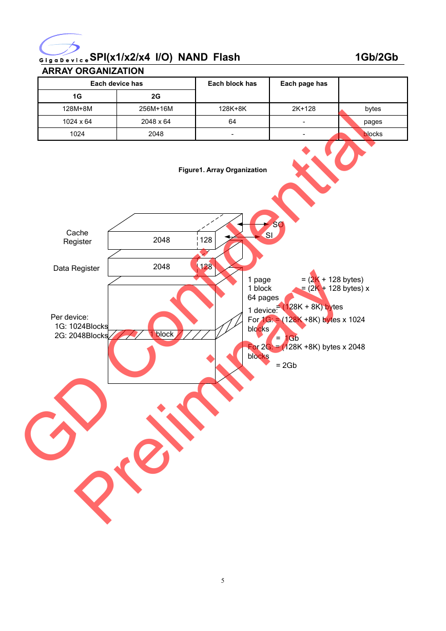
Figure1. Array Organization
Cache
Register
Data Register
2048
2048
128
128
SO
SI
Per device:
1G: 1024Blocks
2G: 2048Blocks
1 block
= (2K + 128 bytes)
= (2K + 128 bytes) x
1 page
1 block
64 pages
= (128K + 8K) bytes
1 device:
For 1G: = (128K +8K) bytes x 1024
blocks
= 1Gb
For 2G: = (128K +8K) bytes x 2048
blocks
= 2Gb
5
GD Confidential Preliminary�
SPI(x1/x2/x4 I/O) NAND Flash 1Gb/2Gb
MEMORY MAPPING
< 6 7 8 15 16 >
Blocks
RA
0
1
2
102
3
204
7
Pages
RA<5:0>
0
1
63
Bytes
CA<11:0
>
Note:
0
1
2
217
5
1. CA: Column Address. The 12-bit address is capable of addressing from 0 to 4095 bytes; however, only bytes 0
through 2175 are valid. Bytes 2176 through 4095 of each page are “out of bounds,” do not exist in the device,
and cannot be addressed.
2. RA: Row Address. RA<5:0> selects a page inside a block, and RA selects a block:
RA<15:6> selects a block for 1G;
RA<16:6> selects a block for 2G.
6
GD Confidential Preliminary�
DEVICE OPERATION
SPI Modes
SPI(x1/x2/x4 I/O) NAND Flash 1Gb/2Gb
SPI NAND supports two SPI modes:
• CPOL = 0, CPHA = 0 (Mode 0)
• CPOL = 1, CPHA = 1 (Mode 3)
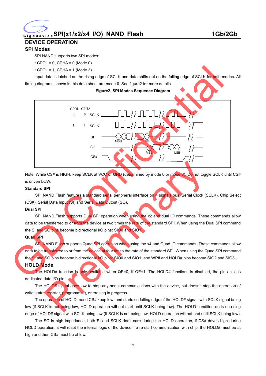
Input data is latched on the rising edge of SCLK and data shifts out on the falling edge of SCLK for both modes. All
timing diagrams shown in this data sheet are mode 0. See figure2 for more details.
Figure2. SPI Modes Sequence Diagram
CPOL CPHA
0
1
0
1
SCLK
SCLK
SI
SO
CS#
MSB
LSB
MSB
LSB
Note: While CS# is HIGH, keep SCLK at VCC or GND (determined by mode 0 or mode 3). Do not toggle SCLK until CS#
is driven LOW.
Standard SPI
SPI NAND Flash features a standard serial peripheral interface on 4 signals bus: Serial Clock (SCLK), Chip Select
(CS#), Serial Data Input (SI) and Serial Data Output (SO).
Dual SPI
SPI NAND Flash supports Dual SPI operation when using the x2 and dual IO commands. These commands allow
data to be transferred to or from the device at two times the rate of the standard SPI. When using the Dual SPI command
the SI and SO pins become bidirectional I/O pins: SIO0 and SIO1.
Quad SPI
SPI NAND Flash supports Quad SPI operation when using the x4 and Quad IO commands. These commands allow
data to be transferred to or from the device at four times the rate of the standard SPI. When using the Quad SPI command
the SI and SO pins become bidirectional I/O pins: SIO0 and SIO1, and WP# and HOLD# pins become SIO2 and SIO3.
HOLD Mode
The HOLD# function is only available when QE=0, If QE=1, The HOLD# functions is disabled, the pin acts as
dedicated data I/O pin.
The HOLD# signal goes low to stop any serial communications with the device, but doesn’t stop the operation of
write status register, programming, or erasing in progress.
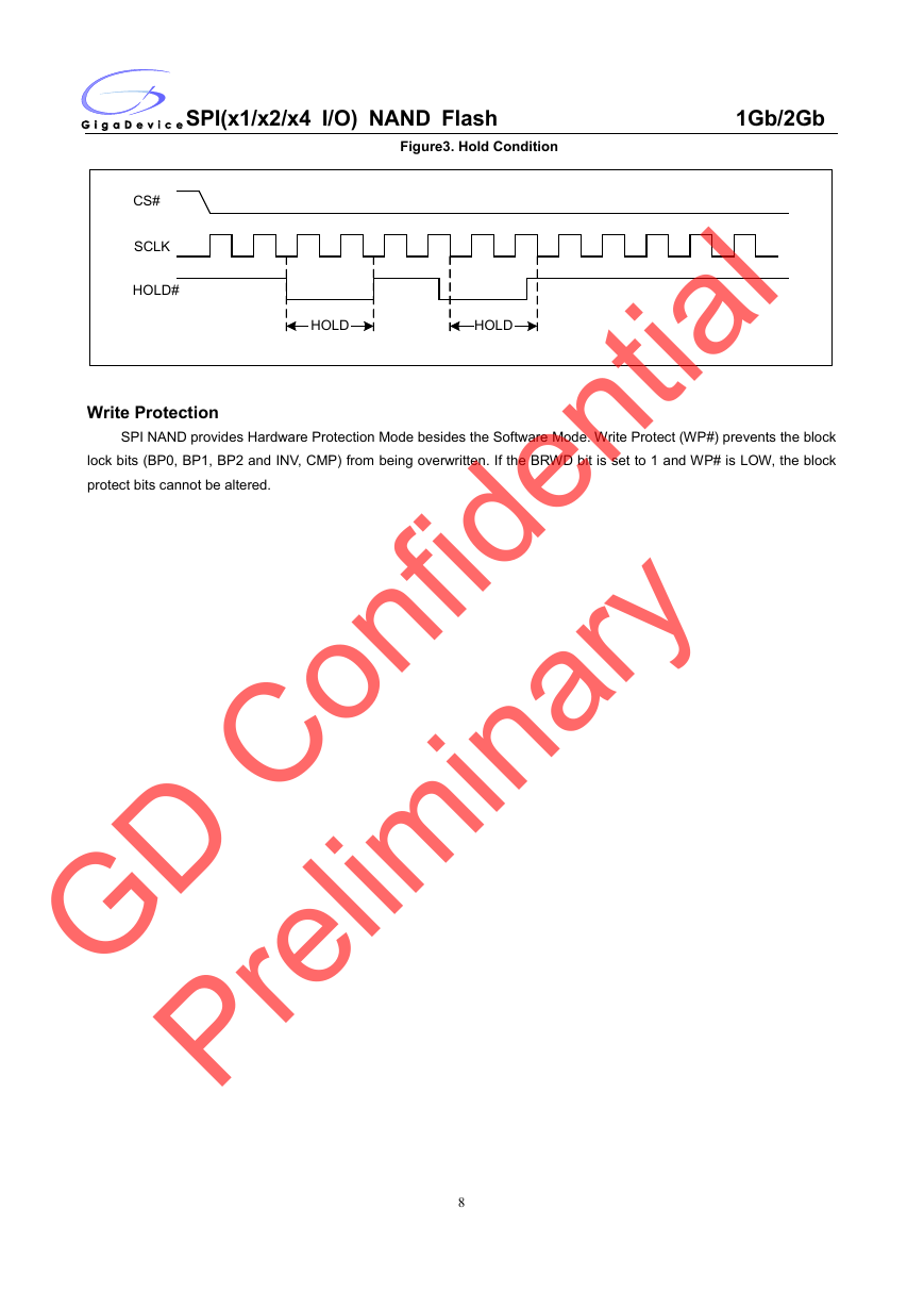
The operation of HOLD, need CS# keep low, and starts on falling edge of the HOLD# signal, with SCLK signal being
low (if SCLK is not being low, HOLD operation will not start until SCLK being low). The HOLD condition ends on rising
edge of HOLD# signal with SCLK being low (If SCLK is not being low, HOLD operation will not end until SCLK being low).
The SO is high impedance, both SI and SCLK don’t care during the HOLD operation, if CS# drives high during
HOLD operation, it will reset the internal logic of the device. To re-start communication with chip, the HOLD# must be at
high and then CS# must be at low.
7
GD Confidential Preliminary�
SPI(x1/x2/x4 I/O) NAND Flash 1Gb/2Gb
Figure3. Hold Condition
CS#
SCLK
HOLD#
HOLD
HOLD
Write Protection
SPI NAND provides Hardware Protection Mode besides the Software Mode. Write Protect (WP#) prevents the block
lock bits (BP0, BP1, BP2 and INV, CMP) from being overwritten. If the BRWD bit is set to 1 and WP# is LOW, the block
protect bits cannot be altered.
8
GD Confidential Preliminary�



 2023年江西萍乡中考道德与法治真题及答案.doc
 2012年重庆南川中考生物真题及答案.doc
 2013年江西师范大学地理学综合及文艺理论基础考研真题.doc
 2020年四川甘孜小升初语文真题及答案I卷.doc
 2020年注册岩土工程师专业基础考试真题及答案.doc
 2023-2024学年福建省厦门市九年级上学期数学月考试题及答案.doc
 2021-2022学年辽宁省沈阳市大东区九年级上学期语文期末试题及答案.doc
 2022-2023学年北京东城区初三第一学期物理期末试卷及答案.doc
 2018上半年江西教师资格初中地理学科知识与教学能力真题及答案.doc
 2012年河北国家公务员申论考试真题及答案-省级.doc
 2020-2021学年江苏省扬州市江都区邵樊片九年级上学期数学第一次质量检测试题及答案.doc
 2022下半年黑龙江教师资格证中学综合素质真题及答案.doc