8-/6-/4-Channel DAS with 16-Bit, Bipolar
Input, Simultaneous Sampling ADC
AD7606/AD7606-6/AD7606-4
FEATURES
8/6/4 simultaneously sampled inputs
True bipolar analog input ranges: ±10 V, ±5 V
Single 5 V analog supply and 2.3 V to 5 V VDRIVE
Fully integrated data acquisition solution
Analog input clamp protection
Input buffer with 1 MΩ analog input impedance
Second-order antialiasing analog filter
On-chip accurate reference and reference buffer
16-bit ADC with 200 kSPS on all channels
Oversampling capability with digital filter
Flexible parallel/serial interface
SPI/QSPI™/MICROWIRE™/DSP compatible
Performance
7 kV ESD rating on analog input channels
95.5 dB SNR, −107 dB THD
±0.5 LSB INL, ±0.5 LSB DNL
Low power: 100 mW
Standby mode: 25 mW
APPLICATIONS
Power-line monitoring and protection systems
Multiphase motor control
Instrumentation and control systems
Multiaxis positioning systems
Data acquisition systems (DAS)
Table 1. High Resolution, Bipolar Input, Simultaneous
Sampling DAS Solutions
Single-
Ended
Inputs
AD7608
AD7606
AD7606-6
AD7606-4
AD7607
True
Differential
Inputs
AD7609
Number of
Simultaneous
Sampling Channels
8
8
6
4
8
Resolution
18 Bits
16 Bits
14 Bits
64-lead LQFP package
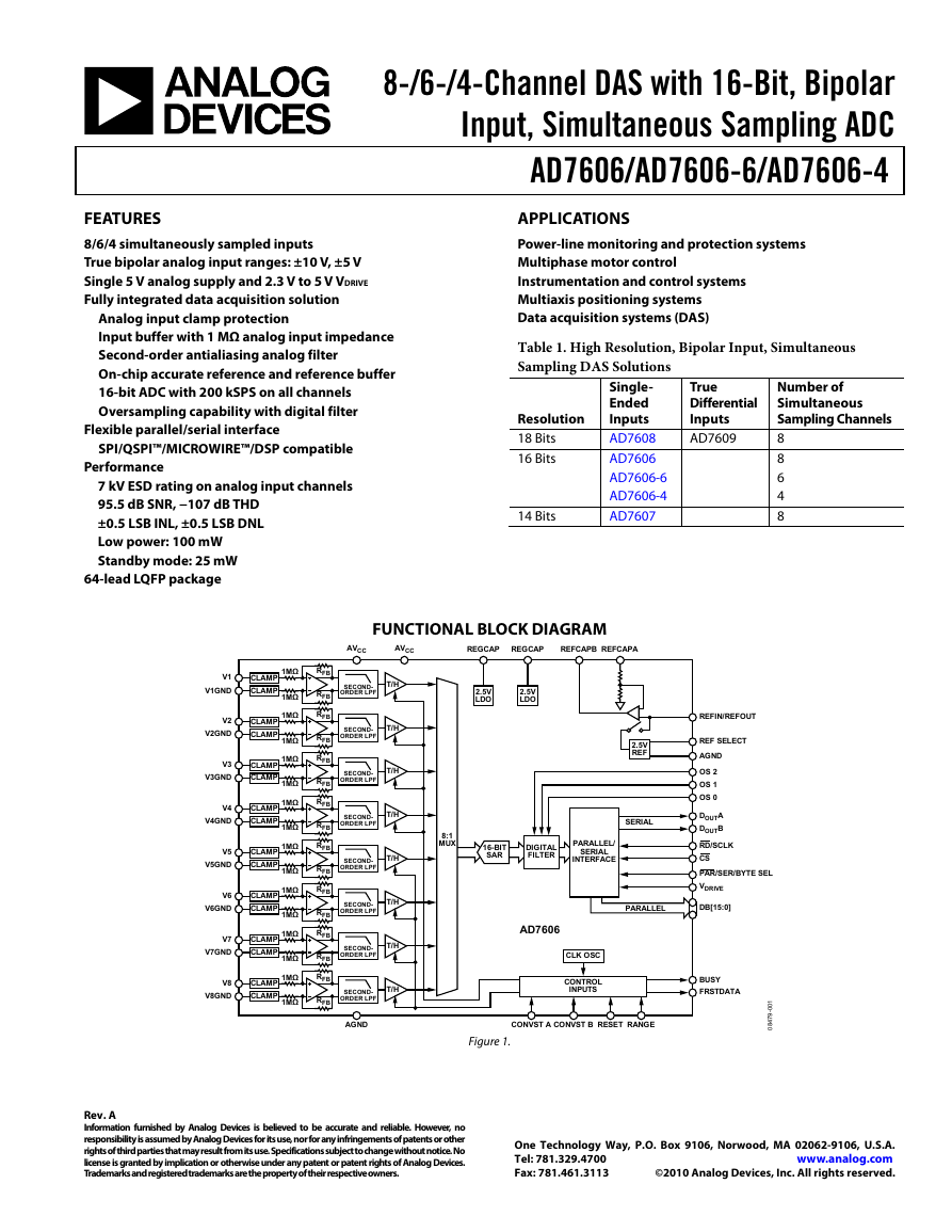
FUNCTIONAL BLOCK DIAGRAM
AVCC
AVCC
REGCAP
REGCAP
REFCAPB REFCAPA
V1
V1GND
CLAMP
CLAMP
V2
V2GND
CLAMP
CLAMP
V3
V3GND
CLAMP
CLAMP
V4
V4GND
CLAMP
CLAMP
V5
V5GND
CLAMP
CLAMP
V6
V6GND
CLAMP
CLAMP
V7
V7GND
CLAMP
CLAMP
V8
V8GND
CLAMP
CLAMP
1MΩ
1MΩ
1MΩ
1MΩ
1MΩ
1MΩ
1MΩ
1MΩ
1MΩ
1MΩ
1MΩ
1MΩ
1MΩ
1MΩ
1MΩ
1MΩ
RFB
RFB
RFB
RFB
RFB
RFB
RFB
RFB
RFB
RFB
RFB
RFB
RFB
RFB
RFB
RFB
T/H
T/H
T/H
T/H
T/H
T/H
T/H
T/H
SECOND-
ORDER LPF
SECOND-
ORDER LPF
SECOND-
ORDER LPF
SECOND-
ORDER LPF
SECOND-
ORDER LPF
SECOND-
ORDER LPF
SECOND-
ORDER LPF
SECOND-
ORDER LPF
AGND
2.5V
LDO
2.5V
LDO
8:1
MUX
16-BIT
SAR
DIGITAL
FILTER
PARALLEL/
INTERFACE
SERIAL
2.5V
REF
SERIAL
REFIN/REFOUT
REF SELECT
AGND
OS 2
OS 1
OS 0
DOUTA
DOUTB
RD/SCLK
CS
PAR/SER/BYTE SEL
VDRIVE
PARALLEL
DB[15:0]
AD7606
CLK OSC
CONTROL
INPUTS
CONVST A CONVST B RESET RANGE
Figure 1.
BUSY
FRSTDATA
1
0
0
-
9
7
4
8
0
Rev. A
Information furnished by Analog Devices is believed to be accurate and reliable. However, no
responsibility is assumed by Analog Devices for its use, nor for any infringements of patents or other
rights of third parties that may result from its use. Specifications subject to change without notice. No
license is granted by implication or otherwise under any patent or patent rights of Analog Devices.
Trademarks and registered trademarks are the property of their respective owners.
One Technology Way, P.O. Box 9106, Norwood, MA 02062-9106, U.S.A.
www.analog.com
Tel: 781.329.4700
©2010 Analog Devices, Inc. All rights reserved.
Fax: 781.461.3113
�
Analog Input ............................................................................... 22
ADC Transfer Function ............................................................. 23
Internal/External Reference ...................................................... 24
Typical Connection Diagram ................................................... 25
Power-Down Modes .................................................................. 25
Conversion Control ................................................................... 26
Digital Interface .............................................................................. 27
Parallel Interface (PAR/SER/BYTE SEL = 0) .......................... 27
Parallel Byte (PAR/SER/BYTE SEL = 1, DB15 = 1) ............... 27
Serial Interface (PAR/SER/BYTE SEL = 1) ............................. 27
Reading During Conversion ..................................................... 28
Digital Filter ................................................................................ 29
Layout Guidelines....................................................................... 32
Outline Dimensions ....................................................................... 34
Ordering Guide .......................................................................... 34
AD7606/AD7606-6/AD7606-4
TABLE OF CONTENTS
Features .............................................................................................. 1
Applications ....................................................................................... 1
Functional Block Diagram .............................................................. 1
Revision History ............................................................................... 2
General Description ......................................................................... 3
Specifications ..................................................................................... 4
Timing Specifications .................................................................. 7
Absolute Maximum Ratings .......................................................... 11
Thermal Resistance .................................................................... 11
ESD Caution ................................................................................ 11
Pin Configurations and Function Descriptions ......................... 12
Typical Performance Characteristics ........................................... 17
Terminology .................................................................................... 21
Theory of Operation ...................................................................... 22
Converter Details ........................................................................ 22
REVISION HISTORY
8/10—Rev. 0 to Rev. A
Changes to Note 1, Table 2 .............................................................. 6
5/10—Revision 0: Initial Version
Rev. A | Page 2 of 36
�
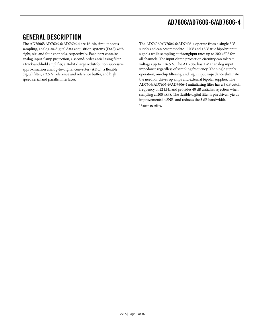
GENERAL DESCRIPTION
The AD76061/AD7606-6/AD7606-4 are 16-bit, simultaneous
sampling, analog-to-digital data acquisition systems (DAS) with
eight, six, and four channels, respectively. Each part contains
analog input clamp protection, a second-order antialiasing filter,
a track-and-hold amplifier, a 16-bit charge redistribution successive
approximation analog-to-digital converter (ADC), a flexible
digital filter, a 2.5 V reference and reference buffer, and high
speed serial and parallel interfaces.
AD7606/AD7606-6/AD7606-4
The AD7606/AD7606-6/AD7606-4 operate from a single 5 V
supply and can accommodate ±10 V and ±5 V true bipolar input
signals while sampling at throughput rates up to 200 kSPS for
all channels. The input clamp protection circuitry can tolerate
voltages up to ±16.5 V. The AD7606 has 1 MΩ analog input
impedance regardless of sampling frequency. The single supply
operation, on-chip filtering, and high input impedance eliminate
the need for driver op amps and external bipolar supplies. The
AD7606/AD7606-6/AD7606-4 antialiasing filter has a 3 dB cutoff
frequency of 22 kHz and provides 40 dB antialias rejection when
sampling at 200 kSPS. The flexible digital filter is pin driven, yields
improvements in SNR, and reduces the 3 dB bandwidth.
1 Patent pending.
Rev. A | Page 3 of 36
�
AD7606/AD7606-6/AD7606-4
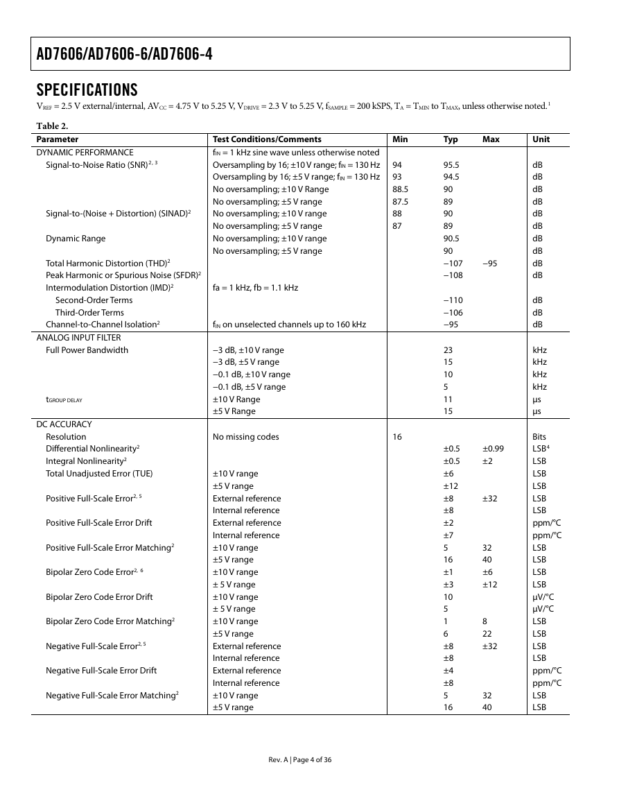
SPECIFICATIONS
VREF = 2.5 V external/internal, AVCC = 4.75 V to 5.25 V, VDRIVE = 2.3 V to 5.25 V, fSAMPLE = 200 kSPS, TA = TMIN to TMAX, unless otherwise noted.1
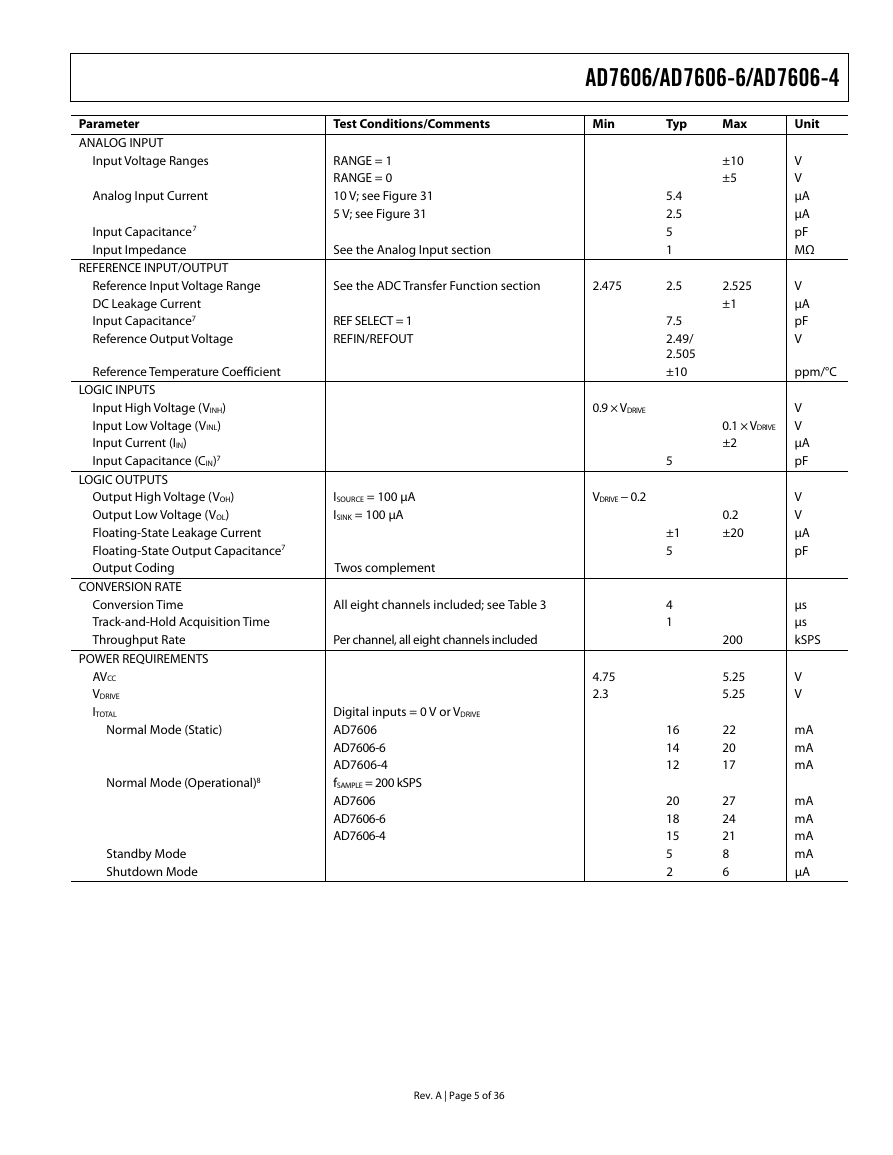
Table 2.
Parameter
DYNAMIC PERFORMANCE
Signal-to-Noise Ratio (SNR)2, 3
Signal-to-(Noise + Distortion) (SINAD)2
Dynamic Range
Total Harmonic Distortion (THD)2
Peak Harmonic or Spurious Noise (SFDR)2
Intermodulation Distortion (IMD)2
Second-Order Terms
Third-Order Terms
Test Conditions/Comments
fIN = 1 kHz sine wave unless otherwise noted
Oversampling by 16; ±10 V range; fIN = 130 Hz 94
Oversampling by 16; ±5 V range; fIN = 130 Hz 93
No oversampling; ±10 V Range
No oversampling; ±5 V range
No oversampling; ±10 V range
No oversampling; ±5 V range
No oversampling; ±10 V range
No oversampling; ±5 V range
fa = 1 kHz, fb = 1.1 kHz
Channel-to-Channel Isolation2 f
IN on unselected channels up to 160 kHz
ANALOG INPUT FILTER
Full Power Bandwidth
tGROUP DELAY
DC ACCURACY
Resolution
Differential Nonlinearity2
Integral Nonlinearity2
Total Unadjusted Error (TUE)
Positive Full-Scale Error2, 5
Positive Full-Scale Error Drift
Positive Full-Scale Error Matching2
Bipolar Zero Code Error2, 6
Bipolar Zero Code Error Drift
Bipolar Zero Code Error Matching2
Negative Full-Scale Error2, 5
Negative Full-Scale Error Drift
Negative Full-Scale Error Matching2
−3 dB, ±10 V range
−3 dB, ±5 V range
−0.1 dB, ±10 V range
−0.1 dB, ±5 V range
±10 V Range
±5 V Range
No missing codes
±10 V range
±5 V range
External reference
Internal reference
External reference
Internal reference
±10 V range
±5 V range
±10 V range
± 5 V range
±10 V range
± 5 V range
±10 V range
±5 V range
External reference
Internal reference
External reference
Internal reference
±10 V range
±5 V range
Rev. A | Page 4 of 36
Min
88.5
87.5
88
87
16
Typ
95.5
94.5
90
89
90
89
90.5
90
−107
−108
−110
−106
−95
23
15
10
5
11
15
±0.5
±0.5
±6
±12
±8
±8
±2
±7
5
16
±1
±3
10
5
1
6
±8
±8
±4
±8
5
16
Max
−95
±0.99
±2
±32
32
40
±6
±12
8
22
±32
32
40
Unit
dB
dB
dB
dB
dB
dB
dB
dB
dB
dB
dB
dB
dB
kHz
kHz
kHz
kHz
μs
μs
Bits
LSB4
LSB
LSB
LSB
LSB
LSB
ppm/°C
ppm/°C
LSB
LSB
LSB
LSB
μV/°C
μV/°C
LSB
LSB
LSB
LSB
ppm/°C
ppm/°C
LSB
LSB
�
Parameter
ANALOG INPUT
Input Voltage Ranges
Analog Input Current
Input Capacitance7
Input Impedance
REFERENCE INPUT/OUTPUT
Reference Input Voltage Range
DC Leakage Current
Input Capacitance7
Reference Output Voltage
Reference Temperature Coefficient
LOGIC INPUTS
Input High Voltage (VINH)
Input Low Voltage (VINL)
Input Current (IIN)
Input Capacitance (CIN)7
LOGIC OUTPUTS
Output High Voltage (VOH)
Output Low Voltage (VOL)
Floating-State Leakage Current
Floating-State Output Capacitance7
Output Coding
CONVERSION RATE
Conversion Time
Track-and-Hold Acquisition Time
Throughput Rate
POWER REQUIREMENTS
AVCC
VDRIVE
ITOTAL
Normal Mode (Static)
Normal Mode (Operational)8 f
Standby Mode
Shutdown Mode
Test Conditions/Comments
RANGE = 1
RANGE = 0
10 V; see Figure 31
5 V; see Figure 31
See the Analog Input section
See the ADC Transfer Function section
REF SELECT = 1
REFIN/REFOUT
ISOURCE = 100 μA
ISINK = 100 μA
Twos complement
All eight channels included; see Table 3
Per channel, all eight channels included
Digital inputs = 0 V or VDRIVE
AD7606
AD7606-6
AD7606-4
SAMPLE = 200 kSPS
AD7606
AD7606-6
AD7606-4
AD7606/AD7606-6/AD7606-4
Min
2.475
0.9 × VDRIVE
VDRIVE − 0.2
4.75
2.3
Typ
5.4
2.5
5
1
2.5
7.5
2.49/
2.505
±10
5
±1
5
4
1
16
14
12
20
18
15
5
2
Max
±10
±5
2.525
±1
0.1 × VDRIVE
±2
0.2
±20
200
5.25
5.25
22
20
17
27
24
21
8
6
Unit
V
V
μA
μA
pF
MΩ
V
μA
pF
V
ppm/°C
V
V
μA
pF
V
V
μA
pF
μs
μs
kSPS
V
V
mA
mA
mA
mA
mA
mA
mA
μA
Rev. A | Page 5 of 36
�
AD7606/AD7606-6/AD7606-4
Parameter
Power Dissipation
Normal Mode (Static)
Normal Mode (Operational)8 f
Standby Mode
Shutdown Mode
Test Conditions/Comments
AD7606
SAMPLE = 200 kSPS
AD7606
AD7606-6
AD7606-4
Min
Typ
80
100
90
75
25
10
Max
115.5
142
126
111
42
31.5
Unit
mW
mW
mW
mW
mW
μW
1 Temperature range for the B version is −40°C to +85°C. The AD7606 is operational up to 125°C with throughput rates ≤ 160 kSPS, and the SNR typically reduces by
0.7 dB at 125°C.
2 See the Terminology section.
3 This specification applies when reading during a conversion or after a conversion. If reading during a conversion in parallel mode with VDRIVE = 5 V, SNR typically reduces by 1.5 dB
and THD by 3 dB.
4 LSB means least significant bit. With ±5 V input range, 1 LSB = 152.58 μV. With ±10 V input range, 1 LSB = 305.175 μV.
5 These specifications include the full temperature range variation and contribution from the internal reference buffer but do not include the error contribution from
the external reference.
6 Bipolar zero code error is calculated with respect to the analog input voltage.
7 Sample tested during initial release to ensure compliance.
8 Operational power/current figure includes contribution when running in oversampling mode.
Rev. A | Page 6 of 36
�
AD7606/AD7606-6/AD7606-4
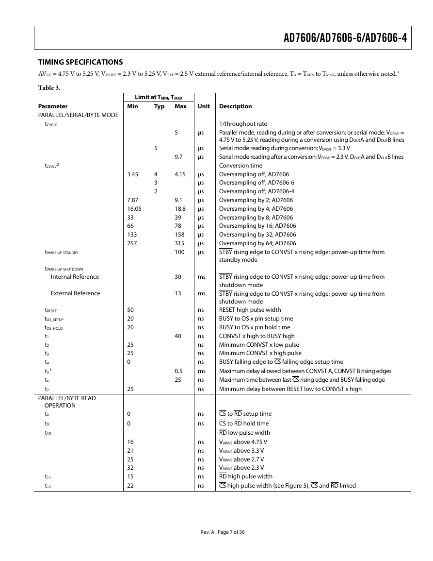
TIMING SPECIFICATIONS
AVCC = 4.75 V to 5.25 V, VDRIVE = 2.3 V to 5.25 V, VREF = 2.5 V external reference/internal reference, TA = TMIN to TMAX, unless otherwise noted.1
Limit at TMIN, TMAX
Typ Max
Unit Description
μs
Table 3.
Parameter
PARALLEL/SERIAL/BYTE MODE
tCYCLE
2
tCONV
tWAKE-UP STANDBY
tWAKE-UP SHUTDOWN
Internal Reference
External Reference
tRESET
tOS_SETUP
tOS_HOLD
t1
t2
t3
t4
t5
3
t6
t7
PARALLEL/BYTE READ
OPERATION
t8
t9
t10
t11
t12
Min
3.45
7.87
16.05
33
66
133
257
50
20
20
25
25
0
25
0
0
16
21
25
32
15
22
5
9.7
4.15
9.1
18.8
39
78
158
315
100
30
13
40
0.5
25
5
4
3
2
μs
μs
μs
μs
μs
μs
μs
μs
μs
μs
μs
μs
ms
ms
ns
ns
ns
ns
ns
ns
ns
ms
ns
ns
ns
ns
ns
ns
ns
ns
ns
ns
1/throughput rate
Parallel mode, reading during or after conversion; or serial mode: VDRIVE =
4.75 V to 5.25 V, reading during a conversion using DOUTA and DOUTB lines
Serial mode reading during conversion; VDRIVE = 3.3 V
Serial mode reading after a conversion; VDRIVE = 2.3 V, DOUTA and DOUTB lines
Conversion time
Oversampling off; AD7606
Oversampling off; AD7606-6
Oversampling off; AD7606-4
Oversampling by 2; AD7606
Oversampling by 4; AD7606
Oversampling by 8; AD7606
Oversampling by 16; AD7606
Oversampling by 32; AD7606
Oversampling by 64; AD7606
STBY rising edge to CONVST x rising edge; power-up time from
standby mode
STBY rising edge to CONVST x rising edge; power-up time from
shutdown mode
STBY rising edge to CONVST x rising edge; power-up time from
shutdown mode
RESET high pulse width
BUSY to OS x pin setup time
BUSY to OS x pin hold time
CONVST x high to BUSY high
Minimum CONVST x low pulse
Minimum CONVST x high pulse
BUSY falling edge to CS falling edge setup time
Maximum delay allowed between CONVST A, CONVST B rising edges
Maximum time between last CS rising edge and BUSY falling edge
Minimum delay between RESET low to CONVST x high
CS to RD setup time
CS to RD hold time
RD low pulse width
VDRIVE above 4.75 V
VDRIVE above 3.3 V
VDRIVE above 2.7 V
VDRIVE above 2.3 V
RD high pulse width
CS high pulse width (see
Figure 5 CS and RD linked
);
Rev. A | Page 7 of 36
�
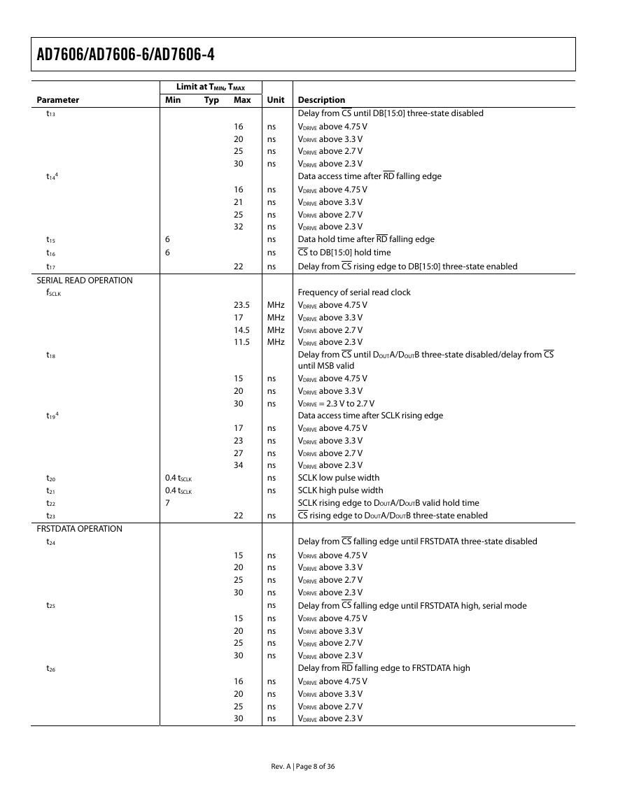
AD7606/AD7606-6/AD7606-4
Parameter
4
t13
t14
t15
t16
t17
SERIAL READ OPERATION
fSCLK
t18
4
t19
t20
t21
t22
t23
FRSTDATA OPERATION
t24
t25
t26
Limit at TMIN, TMAX
Min
6
6
0.4 tSCLK
0.4 tSCLK
7
Typ Max
16
20
25
30
16
21
25
32
22
23.5
17
14.5
11.5
15
20
30
17
23
27
34
22
15
20
25
30
15
20
25
30
16
20
25
30
ns
ns
ns
ns
ns
ns
ns
ns
ns
ns
ns
ns
ns
ns
ns
ns
ns
ns
ns
ns
ns
ns
ns
Unit Description
ns
ns
ns
ns
ns
ns
ns
ns
ns
ns
ns
MHz
MHz
MHz
MHz
Delay from CS until DB[15:0] three-state disabled
VDRIVE above 4.75 V
VDRIVE above 3.3 V
VDRIVE above 2.7 V
VDRIVE above 2.3 V
Data access time after RD falling edge
VDRIVE above 4.75 V
VDRIVE above 3.3 V
VDRIVE above 2.7 V
VDRIVE above 2.3 V
Data hold time after RD falling edge
CS to DB[15:0] hold time
Delay from CS rising edge to DB[15:0] three-state enabled
Frequency of serial read clock
VDRIVE above 4.75 V
VDRIVE above 3.3 V
VDRIVE above 2.7 V
VDRIVE above 2.3 V
Delay from CS until DOUTA/DOUTB three-state disabled/delay from CS
until MSB valid
VDRIVE above 4.75 V
VDRIVE above 3.3 V
VDRIVE = 2.3 V to 2.7 V
Data access time after SCLK rising edge
VDRIVE above 4.75 V
VDRIVE above 3.3 V
VDRIVE above 2.7 V
VDRIVE above 2.3 V
SCLK low pulse width
SCLK high pulse width
SCLK rising edge to DOUTA/DOUTB valid hold time
CS rising edge to DOUTA/DOUTB three-state enabled
Delay from CS falling edge until FRSTDATA three-state disabled
VDRIVE above 4.75 V
VDRIVE above 3.3 V
VDRIVE above 2.7 V
VDRIVE above 2.3 V
Delay from CS falling edge until FRSTDATA high, serial mode
VDRIVE above 4.75 V
VDRIVE above 3.3 V
VDRIVE above 2.7 V
VDRIVE above 2.3 V
Delay from RD falling edge to FRSTDATA high
VDRIVE above 4.75 V
VDRIVE above 3.3 V
VDRIVE above 2.7 V
VDRIVE above 2.3 V
Rev. A | Page 8 of 36
�



 2023年江西萍乡中考道德与法治真题及答案.doc
 2012年重庆南川中考生物真题及答案.doc
 2013年江西师范大学地理学综合及文艺理论基础考研真题.doc
 2020年四川甘孜小升初语文真题及答案I卷.doc
 2020年注册岩土工程师专业基础考试真题及答案.doc
 2023-2024学年福建省厦门市九年级上学期数学月考试题及答案.doc
 2021-2022学年辽宁省沈阳市大东区九年级上学期语文期末试题及答案.doc
 2022-2023学年北京东城区初三第一学期物理期末试卷及答案.doc
 2018上半年江西教师资格初中地理学科知识与教学能力真题及答案.doc
 2012年河北国家公务员申论考试真题及答案-省级.doc
 2020-2021学年江苏省扬州市江都区邵樊片九年级上学期数学第一次质量检测试题及答案.doc
 2022下半年黑龙江教师资格证中学综合素质真题及答案.doc