Microwave device characterisation using a widefield diamond
microscope
Andrew Horsley,1, 2, ∗ Patrick Appel,1 Janik Wolters,1 Jocelyn Achard,3
Alexandre Tallaire,3 Patrick Maletinsky,1, † and Philipp Treutlein1
1Departement Physik, Universit¨at Basel, CH-4056 Switzerland
2Laser Physics Centre, Research School of Physics and Engineering,
Australian National University, 2601 Canberra, Australia
3Laboratoire des Sciences des Proc´ed´es et des Mat´eriaux (LSPM),
CNRS, Universit´e Paris 13, Sorbonne Paris Cit´e,
99 avenue J.B. Cl´ement, 93430 Villetaneuse, France
(Dated: February 22, 2018)
Abstract
Devices relying on microwave circuitry form a cornerstone of many classical and emerging quan-
tum technologies. A capability to provide in-situ, noninvasive and direct imaging of the microwave
fields above such devices would be a powerful tool for their function and failure analysis. In this
work, we build on recent achievements in magnetometry using ensembles of nitrogen vacancy cen-
tres in diamond, to present a widefield microwave microscope with few-micron resolution over a
millimeter-scale field of view, 130 nT Hz−1/2 microwave amplitude sensitivity, a dynamic range of
48 dB, and sub-ms temporal resolution. We use our microscope to image the microwave field a few
microns above a range of microwave circuitry components, and to characterise a novel atom chip
design. Our results open the way to high-throughput characterisation and debugging of complex,
multi-component microwave devices, including real-time exploration of device operation.
8
1
0
2
b
e
F
1
2
]
h
p
-
t
n
a
u
q
[
1
v
2
0
4
7
0
.
2
0
8
1
:
v
i
X
r
a
1
�
Microwave (MW) devices play a critical role in telecommunications, defence, and quantum
technologies. Device characterisation via high resolution MW field imaging is a long-standing
goal [1–3], which promises to overcome the limitations of conventional characterisation tech-
niques. For example, it is difficult to identify internal features of complex devices using S-
parameter measurements of reflection and transmission through external device ports [4, 5].
A high-throughput MW imaging method would allow for fast prototype iteration, and for
more adventurous development of novel device architectures. Furthermore, MW imaging
is of interest for spin-wave imaging in magnonic systems [6, 7], is under investigation for
medical imaging [8, 9], and can be used to characterise materials [10] and biological sam-
ples [11].
In recent years, alkali vapor cells with atoms in the ground [12–16] or highly
excited Rydberg [17–19] states, and nitrogen-vacancy (NV) centres in diamond [20–23] have
shown promise for intrinsically calibrated MW imaging in simple, vacuum- and cryogen-
free environments. Ensembles of NVs in a widefield diamond microscope [24–28] provide
an excellent balance between the wide field of view (FOV) offered by vapor cells and the
nanoscale spatial resolution of single NV centres [29], and so far have been primarily em-
ployed for imaging static and low-frequency magnetic fields. In this work, we demonstrate
high-throughput widefield diamond microscopy for MW device characterisation, enabled by
a step-change we have achieved in microscope performance.
Our microscope integrates advances in camera speed, experiment control, novel diamond
material, laser illumination, and the use of an intrinsically calibrated MW sensing scheme,
to perform MW imaging with an unprecedented combination of temporal resolution, FOV
and spatial resolution. We demonstrate a ∼0.5 mm2 FOV with few-micron spatial reso-
lution, a MW amplitude sensitivity of 130 nT Hz−1/2, and a dynamic range of 48 dB. We
have advanced the temporal resolution to the sub-ms regime, an order of magnitude be-
yond the previous state of the art [22], enabling dynamic probing of circuit operation,
and real-time exploration of large-scale devices by scanning them under the microscope
(Supplementary Movies 1,2). In addition, the accessible design of our microscope enables
high-throughput measurements with rapid exchange of MW devices, demonstrating its ap-
plicability to industry-relevant environments.
2
�
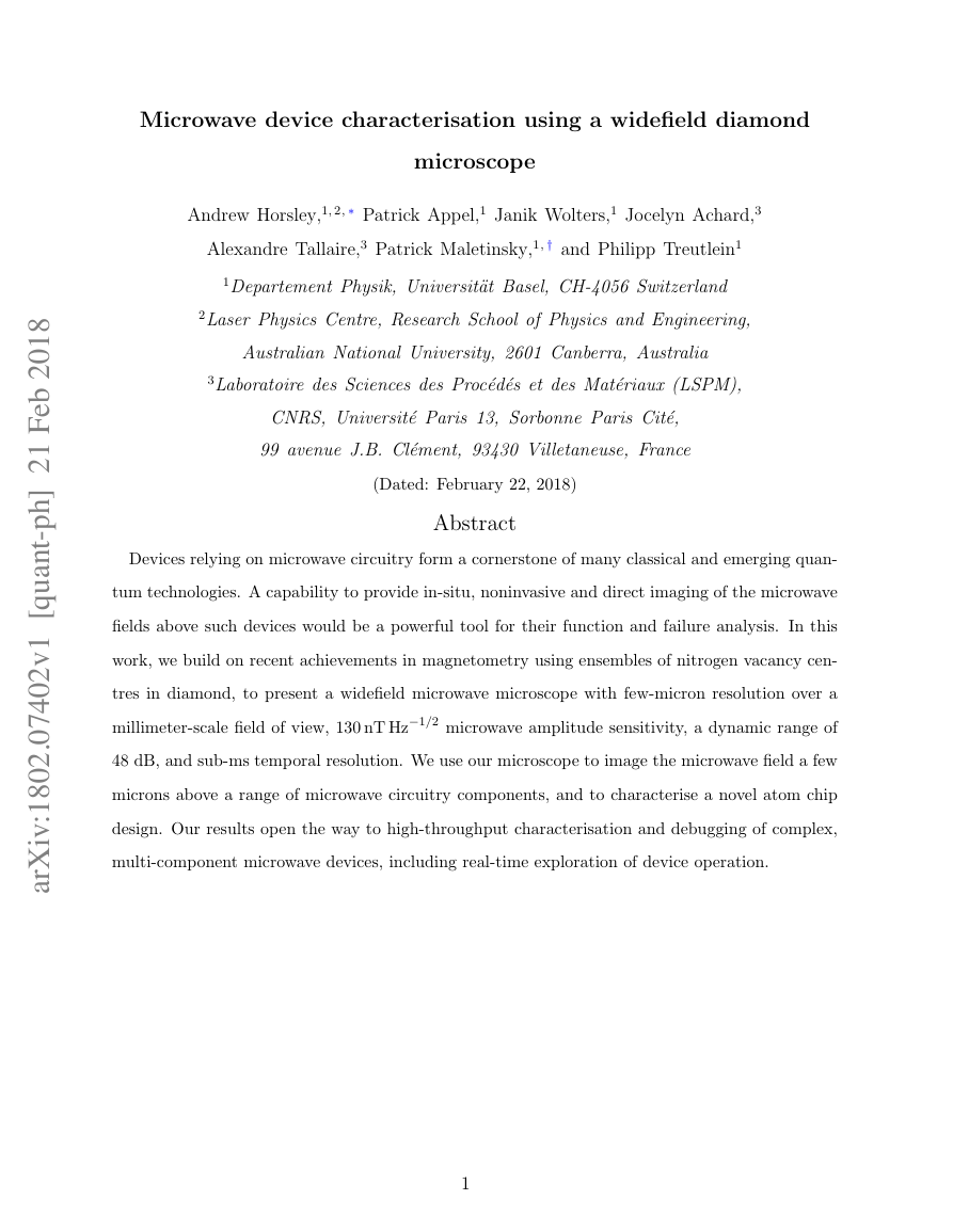
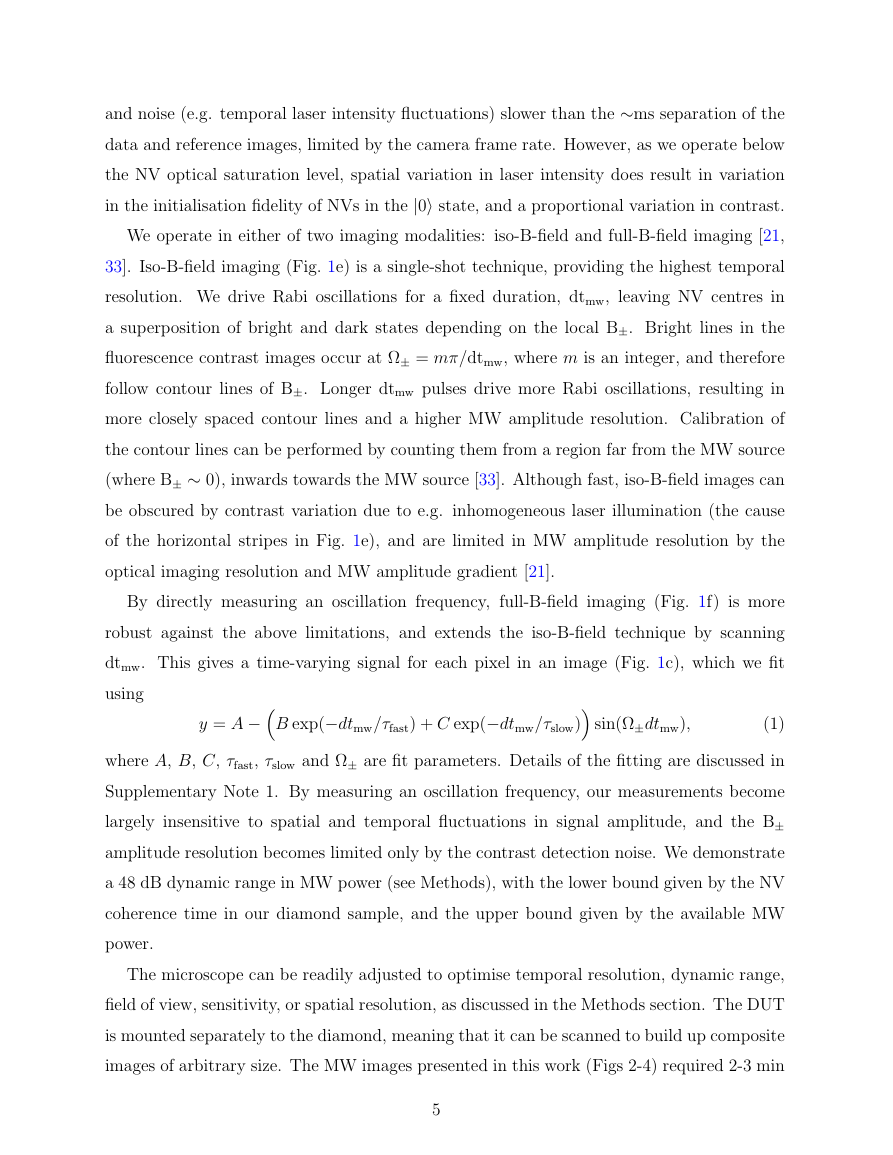
FIG. 1. Widefield diamond microscope and MW imaging technique. (a) Schematic of the MW
imaging setup. We performed imaging using NVs aligned along the (111) axis, tilted 29.5◦ from
the vertical in the XZ plane. (b) NV centre ground state level structure, showing the σ± polarised
MW transitions. (c) Rabi oscillations driven by a MW magnetic field between bright (|0) and
dark (| + 1 or |− 1) fluorescing states. A fit using Eq. 1 is shown in red. (d) Full-B-field imaging
sequence. (e) Iso-B-field imaging mode, revealing the contours of the MW magnetic field. Images
are shown for MW pulses of varying length (dtmw). Horizontal streaks are due to spatial variation
in the 532 nm laser intensity. (f ) Full-B-field image, obtained from a sequence of iso-B-field images
where dtmw is scanned, yielding a time-domain Rabi oscillation signal for each pixel (as shown in
(c)). Pixel-wise fitting then yields an image of the MW magnetic field.
MICROWAVE IMAGING WITH THE WIDEFIELD DIAMOND MICROSCOPE
Our imaging goal is to determine the spatial profile of an inhomogeneous MW field of
known frequency. We perform measurements by driving oscillations on an NV MW transition
and measuring the oscillation frequency, which is proportional to the MW magnetic field
amplitude. At the core of our microscope is a diamond containing a high-density layer
of NV centres that can be brought in close proximity to a microwave device (Fig. 1a).
3
0200400600800246dtmw (s)0.90.920.941-C-=2(1.8510.002) MHzB-=(66.100.08) TNV layerNV uorescence to sCMOS cameramicrowave deviceon XYZ scanning stagelaser light sheet(113) oriented diamond29.5ºNV axisYXZLaserCamera exposure()Nshotsdata imagedtwaitreference imageLaserCamera exposure()Nshotsscan dtmwglobal repeatdtmwdtwaitdtmw|-|+|0ΥNVBdc2.87 GHzabcd0.080.10.120.14Cm100m100m100ef30 dBmIso-B-eld imagingFull-B-eld imagingdtmw = 177 nsdtmw = 252 nsdtmw = 102 nsm200T)B- (�
In our particular setup, we use a (113) oriented diamond with a ∼25 µm thick high density
(4×1014 cm−3) layer of NV centres preferentially oriented along the (111) axis, i.e. oriented at
a 29.5◦ angle from the diamond surface normal (see Methods) [30]. NV centres are optically
active lattice defects in diamond, with an electronic spin-1 ground state (Fig. 1b) [31, 32].
Excitation with 532 nm laser light stimulates state-dependent fluorescence, and pumps the
NV population into the brightly fluorescing |0 state. To optimise the FOV for a given
laser power, we excite the NVs using an in-plane sheet of 532 nm laser light (Fig. 1a, see
Methods). The |0 state is coupled to the darker | ± 1 states by MW magnetic dipole
transitions. To detect MW fields, we first apply a dc magnetic field (Bdc) to tune one of
the ground state MW transitions into resonance with the MW frequency of interest. Using
an appropriate pulse sequence (see below), we then measure the coherent Rabi oscillations
driven by the MW between the coupled states, from which we extract the Rabi frequency
(Fig. 1.c) [20, 33]. Measurements are polarisation-resolved, as each transition is sensitive
to only a single polarisation component of the MW magnetic field, B± for the respective
σ± (|0 → | ± 1) transitions, with the polarisation quantisation axis parallel to the NV
axis (see Methods). A single NV axis can be used to measure both B+ and B− at a given
frequency, by reversing the Bdc direction in turn to tune each of the σ± transitions to the
desired resonance frequency. Our measurements are intrinsically calibrated, as the Rabi
oscillation frequency, Ω±, is related to the MW amplitude by B± = Ω±/(2πγNV), through
the well-characterised NV gyromagnetic ratio, γNV = 28 kHz/µT.
We perform imaging by taking a series of data and reference images (Fig. 1.d). The data
image sequence consists of a single (700 ns) laser pulse, followed by a single MW pulse input
to the MW device under test (DUT). A wait time of dtwait = 1.5 µs between the laser and
MW pulses allows for relaxation of the optically excited NV electron through a metastable
state. This sequence is repeated Nshots ≈ 100 times during a single camera exposure to
accumulate fluorescence counts. The laser pulse both reads out the state of the NVs after
the previous MW pulse, and prepares the NVs in the |0 state before the next MW pulse.
We then take a reference image, with a sequence identical to the data image, but with the
MW off. The data and reference images are combined pixel-wise to create a contrast image
of the relative change in fluorescence induced by the microwave pulse, C = 1 − Ndata/Nref,
where Ndata (Nref) is the fluorescence counts for a given data (reference) pixel. The use of a
reference image reduces the sensitivity to spatial variation in fluorescence collection efficiency
4
�
and noise (e.g. temporal laser intensity fluctuations) slower than the ∼ms separation of the
data and reference images, limited by the camera frame rate. However, as we operate below
the NV optical saturation level, spatial variation in laser intensity does result in variation
in the initialisation fidelity of NVs in the |0 state, and a proportional variation in contrast.
We operate in either of two imaging modalities: iso-B-field and full-B-field imaging [21,
33]. Iso-B-field imaging (Fig. 1e) is a single-shot technique, providing the highest temporal
resolution. We drive Rabi oscillations for a fixed duration, dtmw, leaving NV centres in
a superposition of bright and dark states depending on the local B±. Bright lines in the
fluorescence contrast images occur at Ω± = mπ/dtmw, where m is an integer, and therefore
follow contour lines of B±. Longer dtmw pulses drive more Rabi oscillations, resulting in
more closely spaced contour lines and a higher MW amplitude resolution. Calibration of
the contour lines can be performed by counting them from a region far from the MW source
(where B± ∼ 0), inwards towards the MW source [33]. Although fast, iso-B-field images can
be obscured by contrast variation due to e.g. inhomogeneous laser illumination (the cause
of the horizontal stripes in Fig. 1e), and are limited in MW amplitude resolution by the
optical imaging resolution and MW amplitude gradient [21].
By directly measuring an oscillation frequency, full-B-field imaging (Fig. 1f) is more
robust against the above limitations, and extends the iso-B-field technique by scanning
dtmw. This gives a time-varying signal for each pixel in an image (Fig. 1c), which we fit
B exp(−dtmw/τfast) + C exp(−dtmw/τslow)
sin(Ω±dtmw),
(1)
where A, B, C, τfast, τslow and Ω± are fit parameters. Details of the fitting are discussed in
Supplementary Note 1. By measuring an oscillation frequency, our measurements become
largely insensitive to spatial and temporal fluctuations in signal amplitude, and the B±
amplitude resolution becomes limited only by the contrast detection noise. We demonstrate
a 48 dB dynamic range in MW power (see Methods), with the lower bound given by the NV
coherence time in our diamond sample, and the upper bound given by the available MW
power.
The microscope can be readily adjusted to optimise temporal resolution, dynamic range,
field of view, sensitivity, or spatial resolution, as discussed in the Methods section. The DUT
is mounted separately to the diamond, meaning that it can be scanned to build up composite
images of arbitrary size. The MW images presented in this work (Figs 2-4) required 2-3 min
5
using
y = A −
�
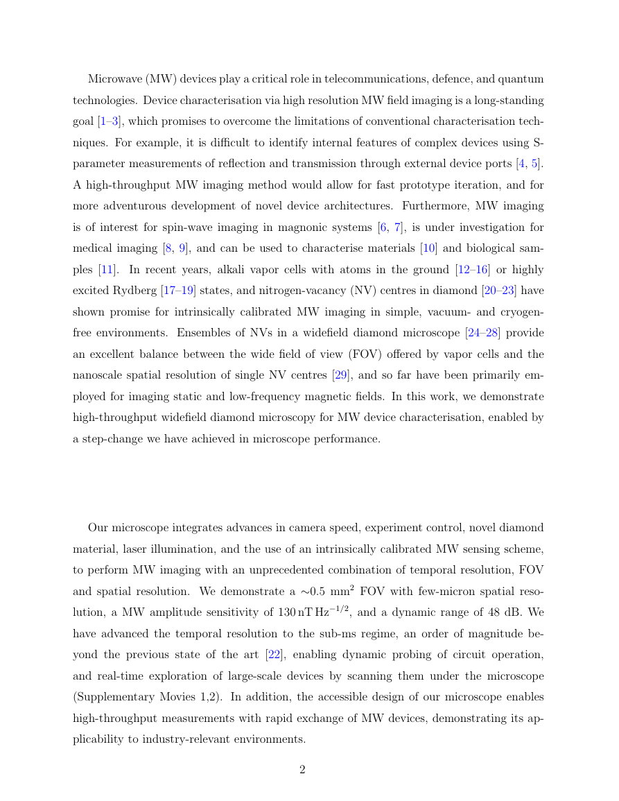
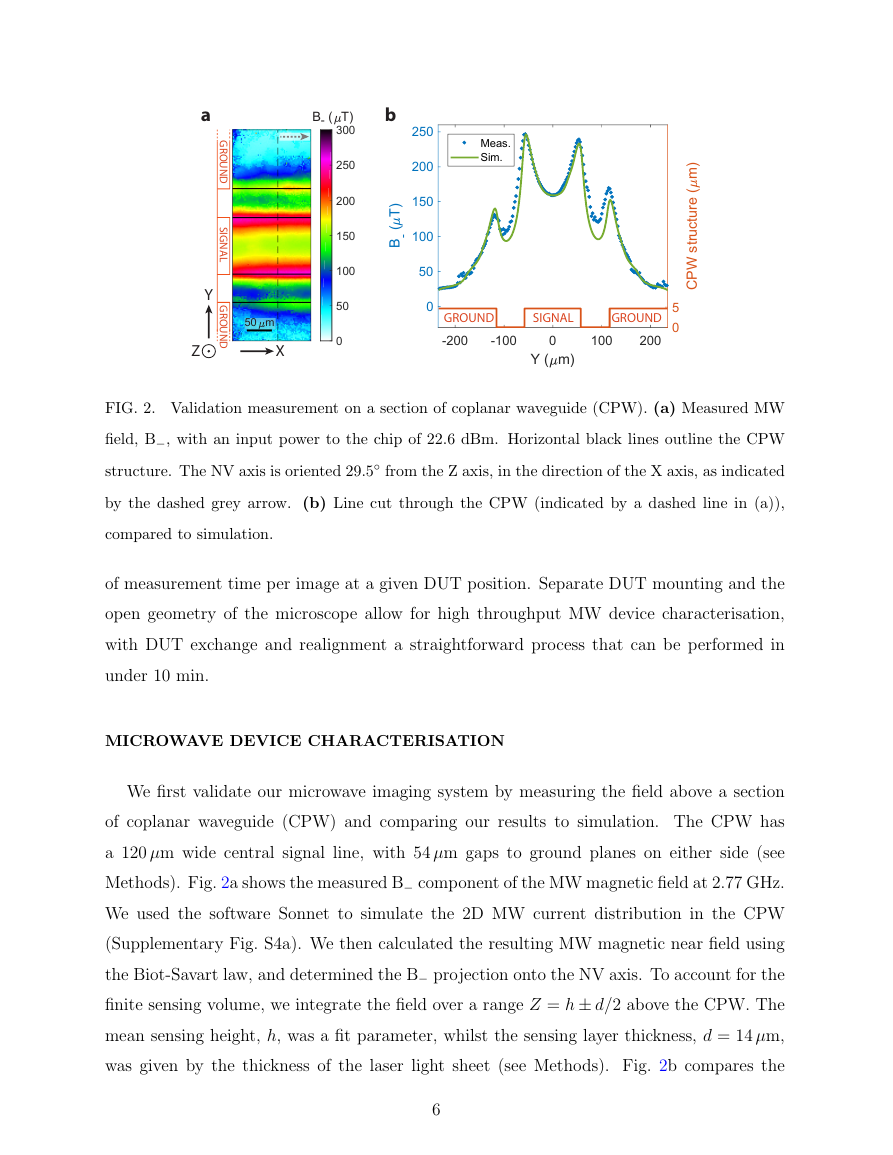
FIG. 2. Validation measurement on a section of coplanar waveguide (CPW). (a) Measured MW
field, B−, with an input power to the chip of 22.6 dBm. Horizontal black lines outline the CPW
structure. The NV axis is oriented 29.5◦ from the Z axis, in the direction of the X axis, as indicated
by the dashed grey arrow. (b) Line cut through the CPW (indicated by a dashed line in (a)),
compared to simulation.
of measurement time per image at a given DUT position. Separate DUT mounting and the
open geometry of the microscope allow for high throughput MW device characterisation,
with DUT exchange and realignment a straightforward process that can be performed in
under 10 min.
MICROWAVE DEVICE CHARACTERISATION
We first validate our microwave imaging system by measuring the field above a section
of coplanar waveguide (CPW) and comparing our results to simulation. The CPW has
a 120 µm wide central signal line, with 54 µm gaps to ground planes on either side (see
Methods). Fig. 2a shows the measured B− component of the MW magnetic field at 2.77 GHz.
We used the software Sonnet to simulate the 2D MW current distribution in the CPW
(Supplementary Fig. S4a). We then calculated the resulting MW magnetic near field using
the Biot-Savart law, and determined the B− projection onto the NV axis. To account for the
finite sensing volume, we integrate the field over a range Z = h ± d/2 above the CPW. The
mean sensing height, h, was a fit parameter, whilst the sensing layer thickness, d = 14 µm,
was given by the thickness of the laser light sheet (see Methods). Fig. 2b compares the
6
050100150200250300-200-1000100200Y (m)050100150200250B- (T)05CPW structure (m)Meas.Sim.abXYSIGNALGROUNDGROUNDZm50T)B- (GROUNDSIGNALGROUND�
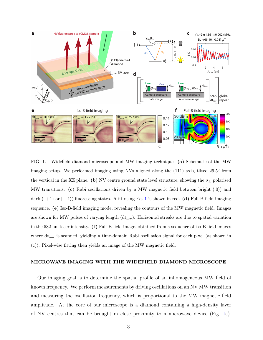
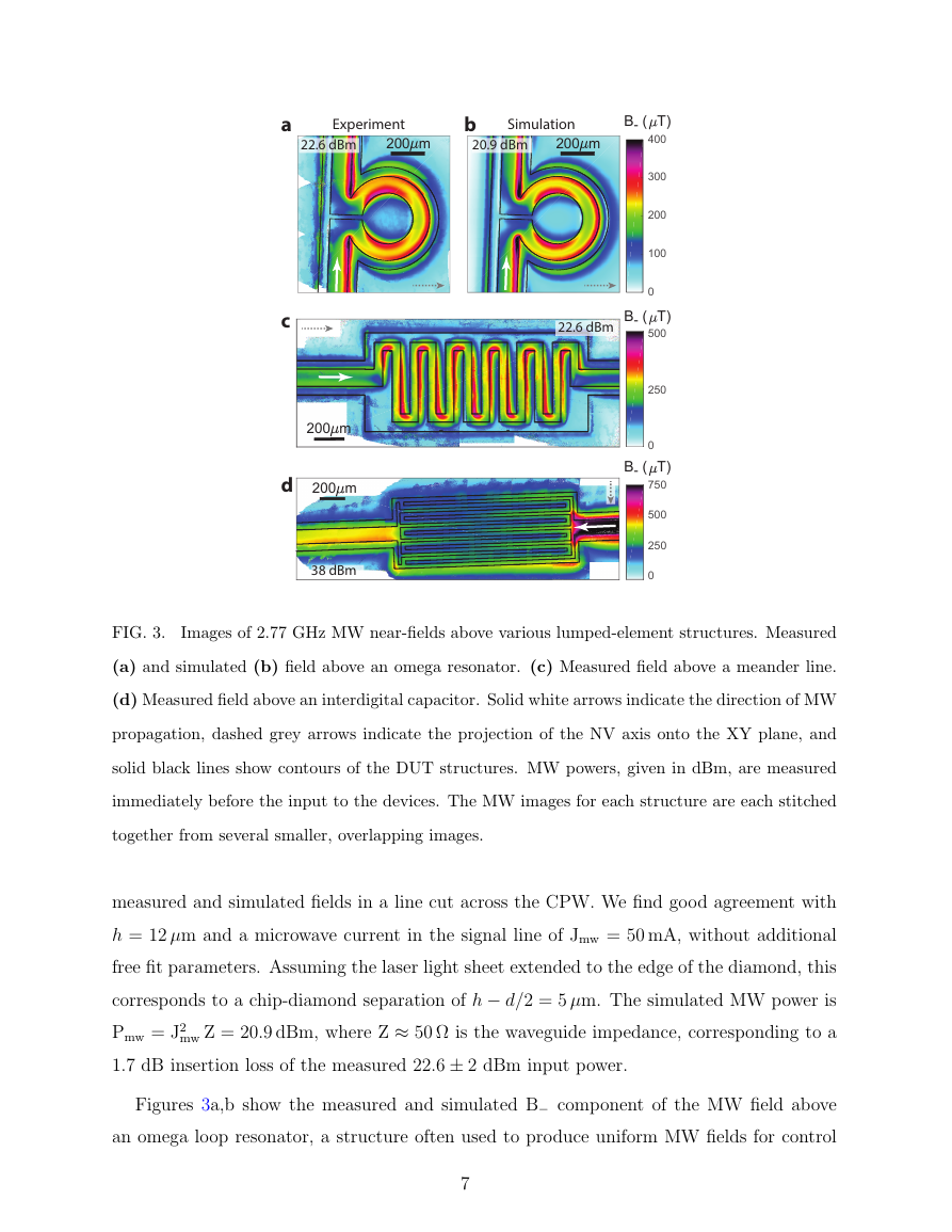
FIG. 3.
Images of 2.77 GHz MW near-fields above various lumped-element structures. Measured
(a) and simulated (b) field above an omega resonator. (c) Measured field above a meander line.
(d) Measured field above an interdigital capacitor. Solid white arrows indicate the direction of MW
propagation, dashed grey arrows indicate the projection of the NV axis onto the XY plane, and
solid black lines show contours of the DUT structures. MW powers, given in dBm, are measured
immediately before the input to the devices. The MW images for each structure are each stitched
together from several smaller, overlapping images.
measured and simulated fields in a line cut across the CPW. We find good agreement with
h = 12 µm and a microwave current in the signal line of Jmw = 50 mA, without additional
free fit parameters. Assuming the laser light sheet extended to the edge of the diamond, this
corresponds to a chip-diamond separation of h − d/2 = 5 µm. The simulated MW power is
mw Z = 20.9 dBm, where Z ≈ 50 Ω is the waveguide impedance, corresponding to a
Pmw = J2
1.7 dB insertion loss of the measured 22.6 ± 2 dBm input power.
Figures 3a,b show the measured and simulated B− component of the MW field above
an omega loop resonator, a structure often used to produce uniform MW fields for control
7
22.6 dBma38 dBmcdT)B- (T)B- (T)B- (bExperimentSimulation02505007500250500m200m200m200m200400300200100022.6 dBm20.9 dBm�
of quantum systems [34]. To achieve the excellent agreement seen between the measured
and simulated fields, we had to impose an asymmetric CPW mode for the feedline to our
simulation (see Supplementary Fig. S4b). We can understand the origin of this asymmetric
current by exploring the MW field in the CPW upstream from the omega loop (see Sup-
plementary Movie 1). Upstream of a 90◦ bend in the CPW, the B− profile is symmetric,
similar to Fig. 2. This indicates that the MW current is also symmetric, as the tilt of the
NV orientation is parallel to the CPW in this section. We saw similar effects in other MW
devices we tested (not shown), and the change from symmetric to asymmetric MW propa-
gation mode is likely due to the difference in inner and outer path lengths around the bend,
which creates a phase mismatch between the ground planes [35]. Note, however, that in
addition to the field asymmetry produced by the MW current asymmetry, some of the B−
asymmetry above the CPW downstream of the 90◦ bend is also due the angle between the
MW current and NV axis.
As a demonstration of the versatility of the microscope, we then imaged B− above an
inductive meander line (Fig. 3c) and an interdigital capacitor (Fig. 3d). Like in the omega
loop, we see that the MW field, and therefore current, is largely confined to edge modes, but
avoids the outer edges of corners. In Fig. 3c, the field features of the meander become blurred
towards the left of the image, due to a 0.25◦ tilt between the diamond and chip increasing
the mean sensing distance from h = 11 µm on the right hand side of the image, to h = 20 µm
on the left hand side. In Fig. 3d, we see that the majority of the MW current is reflected
at the CPW-capacitor interface. To increase the signal in the capacitor fingers, we input
a relatively large Pmw = 38 dBm. The image shows that capacitive coupling does indeed
transfer some MW current from the upstream to downstream fingers, however a significant
current bypasses the capacitor fingers, flowing the through the ground planes surrounding
the finger structure.
In Fig. 4a, we present a prototype design of a novel atom chip, which is a type of device
used for trapping and manipulating ultracold atoms, and a key platform for practical ap-
plications of quantum technologies that exploit such atoms [36]. We use our microscope to
perform an initial characterisation, confirming that the chip provides an all-MW trapping
potential, a new addition to the atom chip toolbox that will enable e.g. chip-generated
trapping of atoms in hyperfine states untrappable using static fields [37, 38]. The trapping
potential, a minimum in the MW field above the chip, is created by counter-propagating
8
�


 2023年江西萍乡中考道德与法治真题及答案.doc
 2012年重庆南川中考生物真题及答案.doc
 2013年江西师范大学地理学综合及文艺理论基础考研真题.doc
 2020年四川甘孜小升初语文真题及答案I卷.doc
 2020年注册岩土工程师专业基础考试真题及答案.doc
 2023-2024学年福建省厦门市九年级上学期数学月考试题及答案.doc
 2021-2022学年辽宁省沈阳市大东区九年级上学期语文期末试题及答案.doc
 2022-2023学年北京东城区初三第一学期物理期末试卷及答案.doc
 2018上半年江西教师资格初中地理学科知识与教学能力真题及答案.doc
 2012年河北国家公务员申论考试真题及答案-省级.doc
 2020-2021学年江苏省扬州市江都区邵樊片九年级上学期数学第一次质量检测试题及答案.doc
 2022下半年黑龙江教师资格证中学综合素质真题及答案.doc