AMBA AXI and ACE Protocol Specification AXI3, AXI4, and AXI4-Lite ACE and ACE-Lite
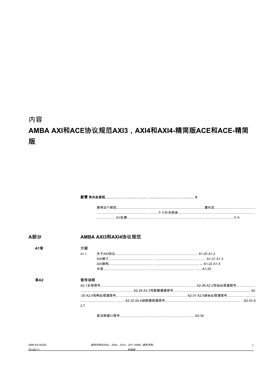
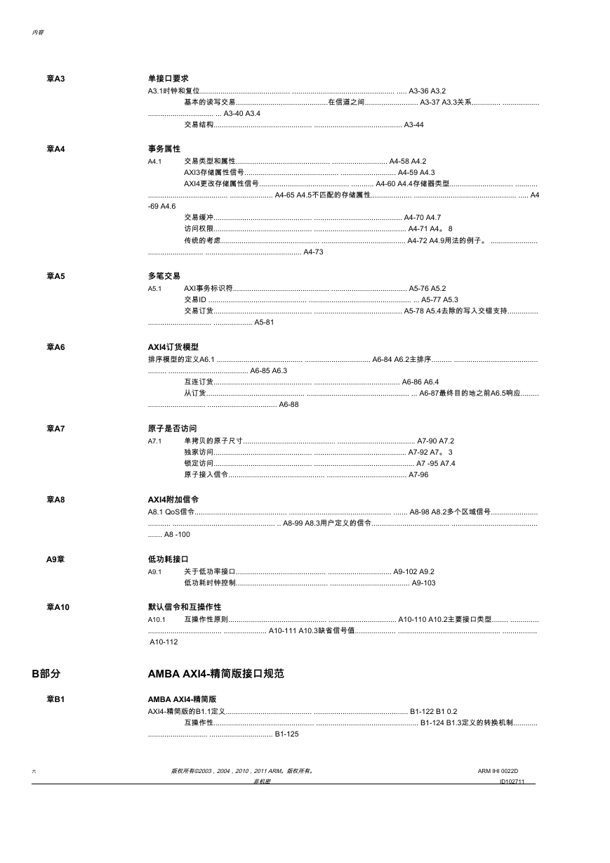
Contents
Preface
About this specification
Intended audience
Using this specification
Part A, AMBA AXI3 and AXI4 Protocol Specification
Part B, AMBA AXI4-Lite Interface Specification
Part C, ACE Protocol Specification
Part D, Appendices
Conventions
Typographic conventions
Timing diagrams
Signals
Numbers
Additional reading
ARM publications
Feedback
Feedback on this specification
Part A: AMBA AXI3 and AXI4 Protocol Specification
A1: Introduction
A1.1 About the AXI protocol
A1.2 AXI revisions
A1.3 AXI Architecture
A1.3.1 Channel definition
A1.3.2 Interface and interconnect
A1.3.3 Register slices
A1.4 Terminology
A1.4.1 AXI components and topology
A1.4.2 AXI transactions, and memory types
A1.4.3 Caches and cache operation
A1.4.4 Temporal description
A2: Signal Descriptions
A2.1 Global signals
A2.2 Write address channel signals
A2.3 Write data channel signals
A2.4 Write response channel signals
A2.5 Read address channel signals
A2.6 Read data channel signals
A2.7 Low-power interface signals
A3: Single Interface Requirements
A3.1 Clock and reset
A3.1.1 Clock
A3.1.2 Reset
A3.2 Basic read and write transactions
A3.2.1 Handshake process
A3.2.2 Channel signaling requirements
A3.3 Relationships between the channels
A3.3.1 Dependencies between channel handshake signals
A3.3.2 Legacy considerations
A3.4 Transaction structure
A3.4.1 Address structure
A3.4.2 Pseudocode description of the transfers
A3.4.3 Data read and write structure
A3.4.4 Read and write response structure
A4: Transaction Attributes
A4.1 Transaction types and attributes
A4.2 AXI3 memory attribute signaling
A4.3 AXI4 changes to memory attribute signaling
A4.3.1 AxCACHE[1], Modifiable
A4.3.2 Ordering requirements for Non-modifiable transactions
A4.3.3 Updated meaning of Read-allocate and Write-allocate
A4.4 Memory types
A4.4.1 Memory type requirements
A4.5 Mismatched memory attributes
A4.5.1 Changing memory attributes
A4.6 Transaction buffering
A4.7 Access permissions
A4.8 Legacy considerations
A4.9 Usage examples
A4.9.1 Use of Device memory types
A5: Multiple Transactions
A5.1 AXI transaction identifiers
A5.2 Transaction ID
A5.3 Transaction ordering
A5.3.1 Read ordering
A5.3.2 Normal write ordering
A5.3.3 AXI3 write data interleaving
A5.3.4 Read and write interaction
A5.3.5 Interconnect use of transaction identifiers
A5.3.6 Width of transaction ID fields
A5.4 Removal of write interleaving support
A5.4.1 Removal of WID
A5.4.2 Legacy considerations
A6: AXI4 Ordering Model
A6.1 Definition of the ordering model
A6.2 Master ordering
A6.3 Interconnect ordering
A6.4 Slave ordering
A6.5 Response before final destination
A7: Atomic Accesses
A7.1 Single-copy atomicity size
A7.2 Exclusive accesses
A7.2.1 Exclusive access process
A7.2.2 Exclusive access from the perspective of the master
A7.2.3 Exclusive access from the perspective of the slave
A7.2.4 Exclusive access restrictions
A7.2.5 Slaves that do not support exclusive access
A7.3 Locked accesses
A7.4 Atomic access signaling
A7.4.1 Legacy considerations
A8: AXI4 Additional Signaling
A8.1 QoS signaling
A8.1.1 QoS interface signals
A8.1.2 Master considerations
A8.1.3 System considerations
A8.2 Multiple region signaling
A8.2.1 Additional interface signals
A8.3 User-defined signaling
A8.3.1 Signal naming
A8.3.2 Usage considerations
A9: Low-power Interface
A9.1 About the low-power interface
A9.2 Low-power clock control
A9.2.1 Peripheral clock required
A9.2.2 Power-down or power-up handshake
A9.2.3 Acceptance of low-power request
A9.2.4 Denial of a low-power request
A9.2.5 Exiting a low-power state
A9.2.6 Clock control sequence summary
A9.2.7 Combining peripherals in a low-power domain
A10: Default Signaling and Interoperability
A10.1 Interoperability principles
A10.2 Major interface categories
A10.2.1 Read/write interface
A10.2.2 Read-only interface
A10.2.3 Write-only interface
A10.2.4 Memory slaves and peripheral slaves
A10.3 Default signal values
A10.3.1 Master addresses
A10.3.2 Slave addresses
A10.3.3 Memory slaves
A10.3.4 Write transactions
A10.3.5 Read transactions
A10.3.6 Response signaling
A10.3.7 Non-secure and secure accesses
Part B: AMBA AXI4-Lite Interface Specification
B1: AMBA AXI4-Lite
B1.1 Definition of AXI4-Lite
B1.1.1 Signal list
B1.1.2 Bus width
B1.1.3 Write strobes
B1.1.4 Optional signaling
B1.2 Interoperability
B1.2.1 Bridge requirements of AXI4-Lite slaves
B1.2.2 Direct connection requirements of AXI4-Lite slaves
B1.3 Defined conversion mechanism
B1.3.1 Conversion rules
B1.4 Conversion, protection, and detection
B1.4.1 Conversion and protection levels
B1.4.2 Implementation considerations
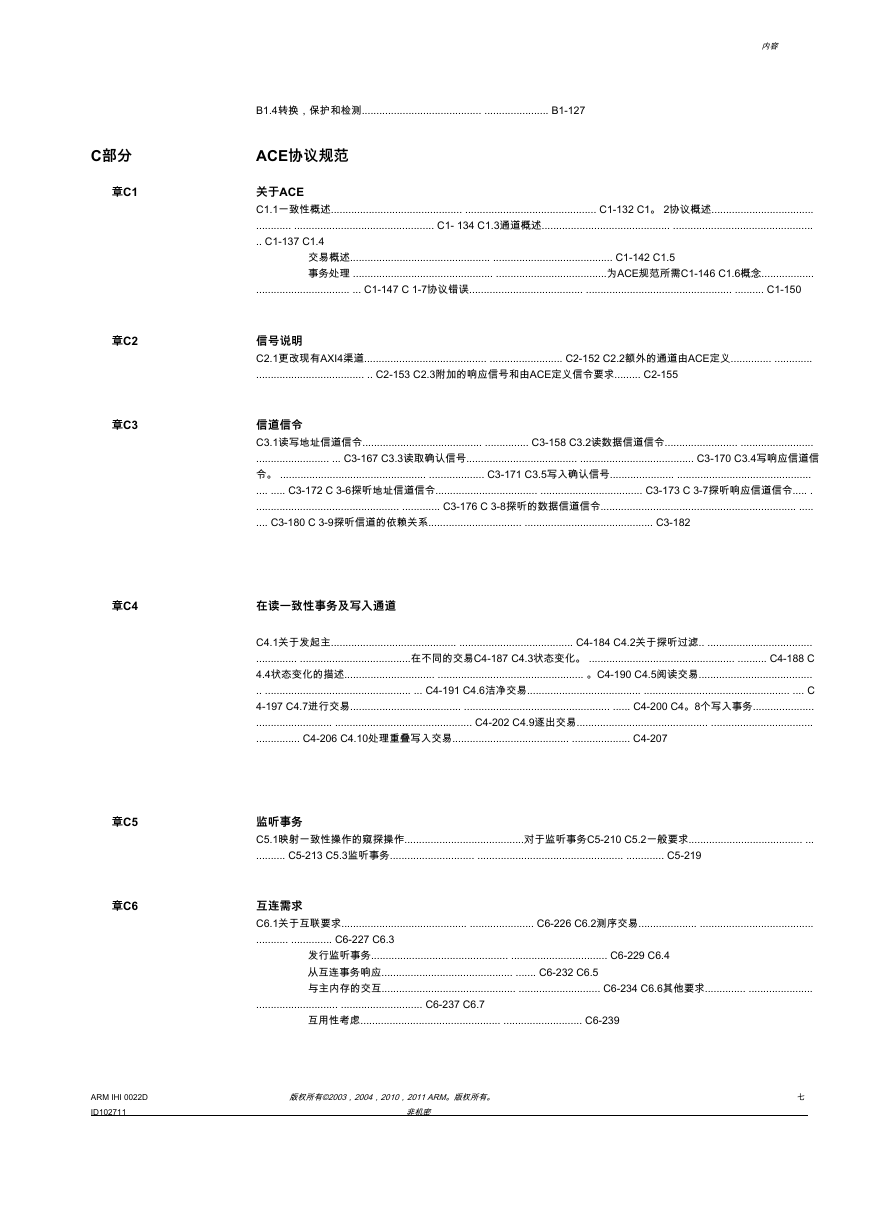
Part C: ACE Protocol Specification
C1: About ACE
C1.1 Coherency overview
C1.1.1 Usage cases
C1.1.2 ACE terminology
C1.2 Protocol overview
C1.2.1 About the ACE protocol
C1.2.2 Coherency model
C1.2.3 Cache state model
C1.3 Channel overview
C1.3.1 Changes to existing AXI4 channels
C1.3.2 Additional channels defined by ACE
C1.3.3 Acknowledge signaling
C1.3.4 Channel usage examples
C1.4 Transaction overview
C1.4.1 Non-snooping transactions
C1.4.2 Coherent transactions
C1.4.3 Memory update transactions
C1.4.4 Cache maintenance transactions
C1.4.5 Snoop transactions
C1.4.6 Barrier transactions
C1.4.7 Distributed virtual memory transactions
C1.5 Transaction processing
C1.6 Concepts required for the ACE specification
C1.6.1 Domains
C1.6.2 Barriers
C1.6.3 Distributed Virtual Memory
C1.7 Protocol errors
C1.7.1 Software protocol error
C1.7.2 Hardware protocol error
C2: Signal Descriptions
C2.1 Changes to existing AXI4 channels
C2.1.1 Read address channel (AR) signals
C2.1.2 Write address channel (AW) signals
C2.1.3 Read data channel (R) signals
C2.2 Additional channels defined by ACE
C2.2.1 Snoop address channel (AC) signals
C2.2.2 Snoop response channel (CR) signals
C2.2.3 Snoop data channel (CD) signals
C2.3 Additional response signals and signaling requirements defined by ACE
C2.3.1 Read acknowledge signal
C2.3.2 Write acknowledge signal
C2.3.3 Additional reset requirements
C3: Channel Signaling
C3.1 Read and write address channel signaling
C3.1.1 Shareability domain types
C3.1.2 Read and write barrier transactions
C3.1.3 Read and write shareable transaction types
C3.1.4 Cache line size restrictions
C3.1.5 Transaction constraints
C3.2 Read data channel signaling
C3.2.1 Read response signaling
C3.3 Read acknowledge signaling
C3.4 Write response channel signaling
C3.5 Write Acknowledge signaling
C3.6 Snoop address channel signaling
C3.6.1 About the snoop address channel
C3.6.2 Snoop address channel signaling
C3.7 Snoop response channel signaling
C3.8 Snoop data channel signaling
C3.9 Snoop channel dependencies
C4: Coherency Transactions on the Read Address and Write Address Channels
C4.1 About an initiating master
C4.1.1 Transaction groups
C4.2 About snoop filtering
C4.3 State changes on different transactions
C4.3.1 State changes associated with a load
C4.3.2 State changes associated with a coherent store
C4.3.3 State changes associated with a main memory update
C4.3.4 State changes associated with cache maintenance operations
C4.4 State change descriptions
C4.5 Read transactions
C4.5.1 ReadNoSnoop
C4.5.2 ReadOnce
C4.5.3 ReadClean
C4.5.4 ReadNotSharedDirty
C4.5.5 ReadShared
C4.5.6 ReadUnique
C4.6 Clean transactions
C4.6.1 CleanUnique
C4.6.2 CleanShared
C4.6.3 CleanInvalid
C4.7 Make transactions
C4.7.1 MakeUnique
C4.7.2 MakeInvalid
C4.8 Write transactions
C4.8.1 WriteNoSnoop
C4.8.2 WriteUnique
C4.8.3 WriteLineUnique
C4.8.4 WriteBack
C4.8.5 WriteClean
C4.8.6 Restrictions on WriteUnique and WriteLineUnique Usage
C4.9 Evict transactions
C4.9.1 Evict
C4.10 Handling overlapping write transactions
C4.10.1 Overlapping ReadUnique
C4.10.2 Overlapping MakeUnique
C4.10.3 Overlapping CleanUnique
C5: Snoop Transactions
C5.1 Mapping coherency operations to snoop operations
C5.1.1 Permitted snoop transactions
C5.1.2 Transactions not permitted as snoop transactions
C5.1.3 Alternative snoop transactions
C5.2 General requirements for snoop transactions
C5.2.1 Channel activity
C5.2.2 Snoop data transfers
C5.2.3 Memory update in progress
C5.2.4 WasUnique snoop response
C5.2.5 Non-blocking requirements for a snooped master
C5.3 Snoop transactions
C5.3.1 ReadOnce
C5.3.2 ReadClean, ReadShared, and ReadNotSharedDirty
C5.3.3 ReadUnique
C5.3.4 CleanInvalid
C5.3.5 MakeInvalid
C5.3.6 CleanShared
C6: Interconnect Requirements
C6.1 About the interconnect requirements
C6.2 Sequencing transactions
C6.2.1 Read and Write Acknowledge
C6.3 Issuing snoop transactions
C6.4 Transaction responses from the interconnect
C6.5 Interactions with main memory
C6.5.1 Interconnect read from main memory or peripheral device
C6.5.2 Main memory update generated by the interconnect
C6.5.3 Permission to update main memory
C6.6 Other requirements
C6.6.1 Non-blocking requirements
C6.6.2 Permitted transaction modifications
C6.6.3 Speculative reads
C6.7 Interoperability considerations
C6.7.1 Cache Line size conversions
C6.7.2 Additional Cache Line conversion considerations
C6.7.3 Address space size
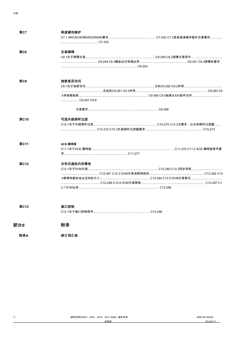
C7: Cache Maintenance
C7.1 ARCACHE and ARDOMAIN requirements
C7.2 Other cache maintenance considerations
C7.2.1 Broadcast cache maintenance requirements
C7.2.2 Requirements for a snooped master
C7.2.3 Processor cache maintenance instructions
C7.2.4 Unpredictable behavior with software cache maintenance
C7.2.5 Mismatched shareability and cacheability
C8: Barrier Transactions
C8.1 About barrier transactions
C8.2 Barrier transaction signaling
C8.2.1 AxBAR signaling
C8.2.2 AxDOMAIN signaling
C8.2.3 Response signaling
C8.3 Barrier responses and domain boundaries
C8.4 Barrier requirements
C8.4.1 Master requirements
C8.4.2 Slave requirements
C8.4.3 Interconnect requirements
C8.4.4 Barriers and Device transaction ordering
C8.4.5 Multi-copy atomicity requirements for shareable locations
C9: Exclusive Accesses
C9.1 About Exclusive accesses
C9.2 Role of the master
C9.2.1 Exclusive Load
C9.2.2 Exclusive Load to Exclusive Store
C9.2.3 Exclusive Store
C9.3 Role of the interconnect
C9.3.1 Minimum PoS Exclusive Monitor
C9.3.2 Additional address comparison
C9.3.3 Multiple interconnect PoS monitors
C9.3.4 PoS Exclusive Monitor behavior
C9.4 Multiple Exclusive Threads
C9.5 Exclusive Accesses from AXI components
C9.6 Transaction requirements
C10: Optional External Snoop Filtering
C10.1 About external snoop filtering
C10.2 Master requirements to support snoop filters
C10.3 External snoop filter requirements
C11: ACE-Lite
C11.1 About ACE-Lite
C11.2 ACE-Lite signal requirements
C12: Distributed Virtual Memory Transactions
C12.1 About DVM transactions
C12.2 Synchronization message
C12.3 DVM transaction process and rules
C12.3.1 DVM Operation process
C12.3.2 DVM Sync and DVM Complete transactions
C12.3.3 Multi-part DVM Operation transactions
C12.3.4 Transaction response
C12.3.5 Message ID
C12.3.6 Instruction cache invalidation alternatives
C12.4 Physical and virtual address space size
C12.4.1 Physical address space size matches virtual address space size
C12.4.2 Physical address space size exceeds virtual address space size
C12.4.3 Virtual address space exceeds physical address space
C12.5 DVM transactions format
C12.6 DVM transaction restrictions
C12.7 DVM Operations
C12.7.1 TLB Invalidate
C12.7.2 Branch Predictor Invalidate
C12.7.3 Physical Instruction Cache Invalidate
C12.7.4 Virtual Instruction Cache Invalidate
C12.7.5 Synchronization
C12.7.6 Hint
C13: Interface Control
C13.1 About the interface control signals
Part D: Appendices
A: Revisions
Glossary



 2023年江西萍乡中考道德与法治真题及答案.doc
 2012年重庆南川中考生物真题及答案.doc
 2013年江西师范大学地理学综合及文艺理论基础考研真题.doc
 2020年四川甘孜小升初语文真题及答案I卷.doc
 2020年注册岩土工程师专业基础考试真题及答案.doc
 2023-2024学年福建省厦门市九年级上学期数学月考试题及答案.doc
 2021-2022学年辽宁省沈阳市大东区九年级上学期语文期末试题及答案.doc
 2022-2023学年北京东城区初三第一学期物理期末试卷及答案.doc
 2018上半年江西教师资格初中地理学科知识与教学能力真题及答案.doc
 2012年河北国家公务员申论考试真题及答案-省级.doc
 2020-2021学年江苏省扬州市江都区邵樊片九年级上学期数学第一次质量检测试题及答案.doc
 2022下半年黑龙江教师资格证中学综合素质真题及答案.doc