Cover
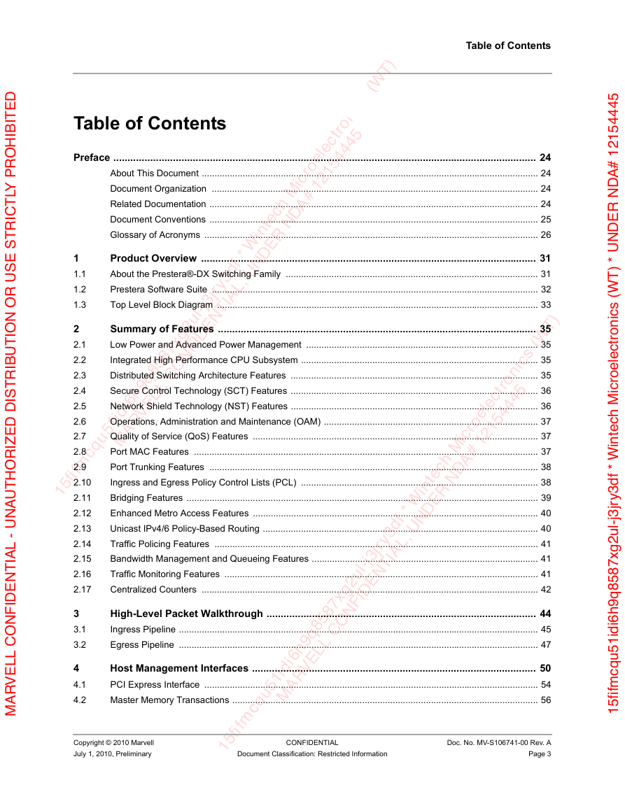
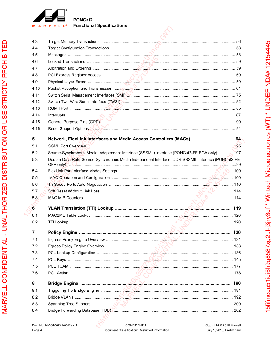
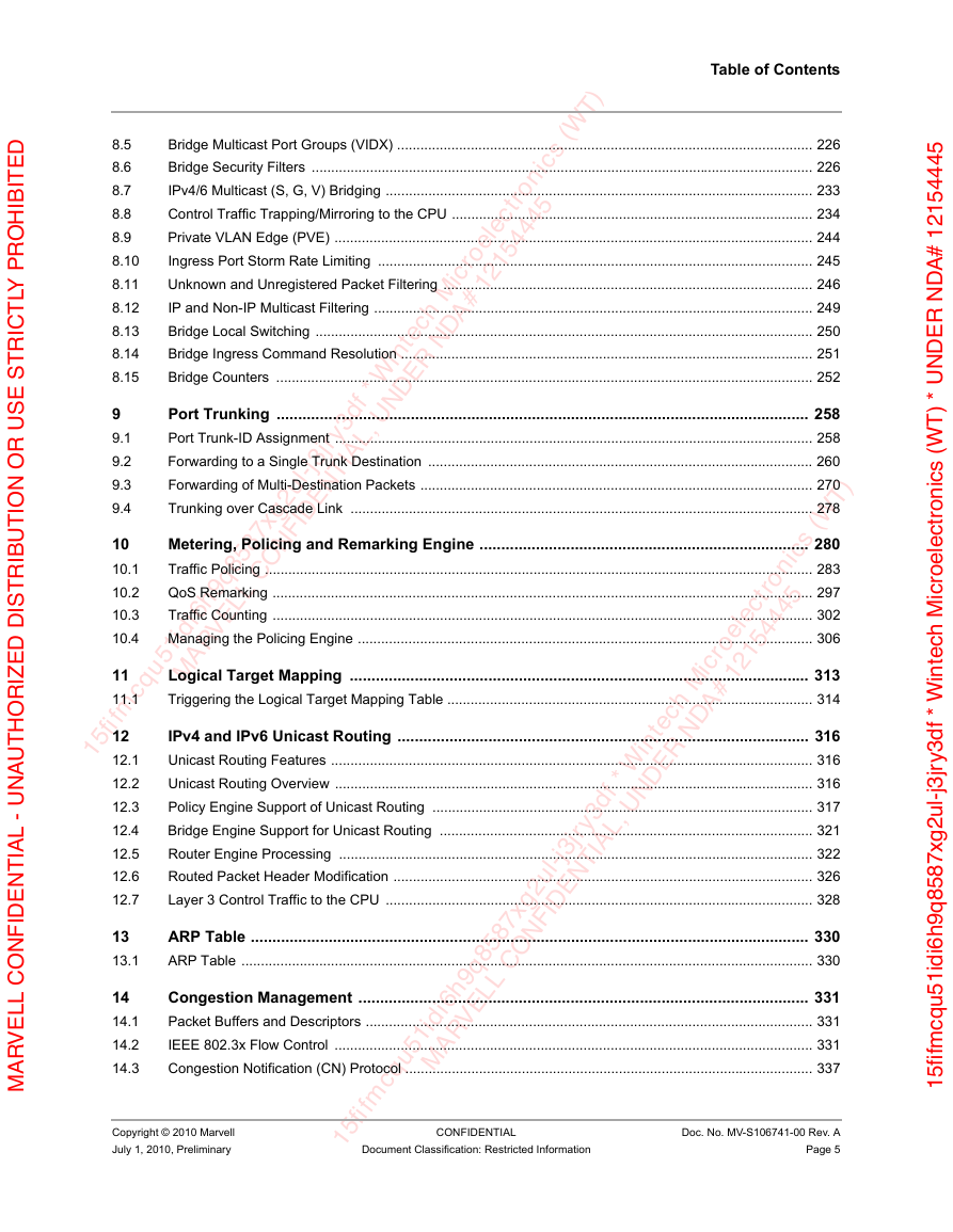
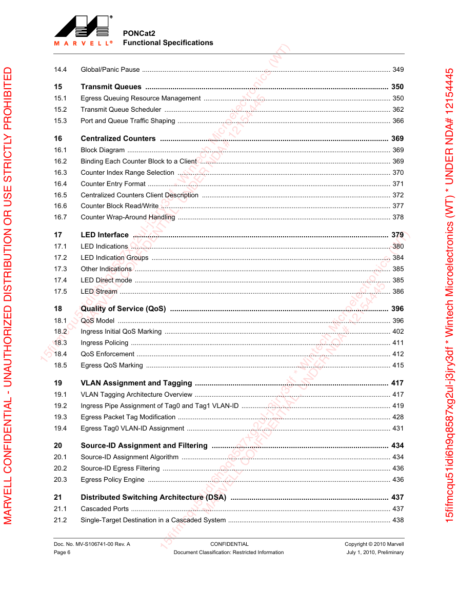
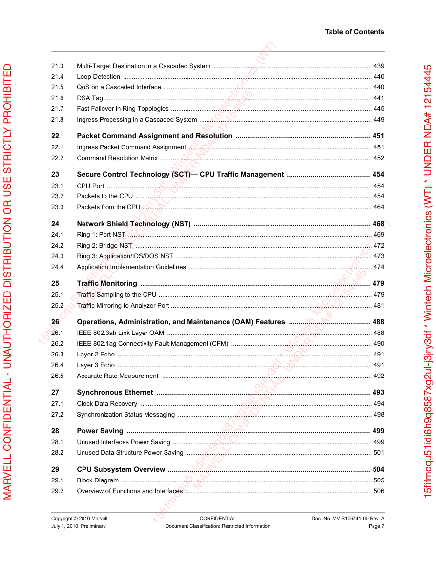
Table of Contents
List of Tables
List of Figures
Preface
About This Document
Document Organization
Related Documentation
Document Conventions
Glossary of Acronyms
1 Product Overview
1.1 About the Prestera®-DX Switching Family
1.1.1 Packet Processor
1.1.2 Integrated CPU
1.2 Prestera Software Suite
1.3 Top Level Block Diagram
2 Summary of Features
2.1 Low Power and Advanced Power Management
2.2 Integrated High Performance CPU Subsystem
2.3 Distributed Switching Architecture Features
2.4 Secure Control Technology (SCT) Features
2.5 Network Shield Technology (NST) Features
2.6 Operations, Administration and Maintenance (OAM)
2.7 Quality of Service (QoS) Features
2.8 Port MAC Features
2.9 Port Trunking Features
2.10 Ingress and Egress Policy Control Lists (PCL)
2.11 Bridging Features
2.12 Enhanced Metro Access Features
2.13 Unicast IPv4/6 Policy-Based Routing
2.14 Traffic Policing Features
2.15 Bandwidth Management and Queueing Features
2.16 Traffic Monitoring Features
2.17 Centralized Counters
Volume 1: Device Walkthrough
3 High-Level Packet Walkthrough
3.1 Ingress Pipeline
3.1.1 Ports MAC Rx
3.1.2 Header Decode Engine
3.1.3 Tunnel-Termination/Interface Classification
3.1.4 Ingress Policy Engine
3.1.5 Bridge Engine
3.1.6 IPv4/v6 Unicast Router Engine
3.1.7 Ingress Policer Engine
3.1.8 Pre-Egress Engine
3.1.8.1 Ingress Pipeline Packet Commands
3.1.8.2 Packet Descriptor Processing
3.2 Egress Pipeline
3.2.1 Egress Filtering
3.2.2 Multi-Target Replication
3.2.3 Descriptor Queueing
3.2.4 Queue and Port Shaping
3.2.5 Transmit Scheduler
3.2.6 Egress Policy Engine
3.2.7 Egress Policer Engine
3.2.8 Ports MAC Tx
4 Host Management Interfaces
4.1 PCI Express Interface
4.1.1 PCI Express Description
4.1.2 PHY Layer
4.1.3 MAC Layer
4.1.4 Data Link Layer
4.1.5 Transaction Layer
4.2 Master Memory Transactions
4.3 Target Memory Transactions
4.3.1 Special Cases
4.3.2 Address Map
4.3.2.1 Internal Regions Mapping
Configuration
4.4 Target Configuration Transactions
4.5 Messages
4.6 Locked Transactions
4.7 Arbitration and Ordering
4.8 PCI Express Register Access
4.8.1 Read Only Register Type
4.8.2 Configuration Header Mapping to Internal Address Space
4.9 Physical Layer Errors
4.9.1 Data Link Layer Errors
4.9.2 Transaction Layer Errors
4.10 Packet Reception and Transmission
4.10.1 Packet Reception (from the Device to the CPU)
Rx SDMA Initialization
Rx SDMA Descriptor Pointer
Rx SDMA Buffer Write Done Interrupt
Rx SDMA Resource Error Event
Rx SDMA Retry/Abort on Resource Error
Rx SDMA Disable Queue Operation
Rx SDMA PCI Express Error Handling
Rx SDMA Parity Error on Data Read from the Device’s Buffers Memory
Rx SDMA Invalid CRC
Rx SDMA Data Byte Order
Configuration
Rx SDMA Counters
Rx SDMA Descriptor
4.10.2 Packet Transmission (from the CPU to the Device)
Tx SDMA Initialization
Tx SDMA Descriptor Pointer
Tx SDMA Buffer Read Done Interrupt
Tx SDMA Resource Error Event
Tx SDMA Recovery from Resource Error
Tx SDMA Disable Queue Operation
Tx SDMA PCI Express Error Handling
Tx SDMA Data Byte Order
Configuration
Tx SDMA Descriptor
4.10.3 Asynchronous Notifications for FDB Update Messages
4.10.3.1 Allocating Host Memory for the Address Update Queue (AUQ) and for FDB Upload Queue (FUQ)
Configuration
4.10.3.2 AUQ Forwarding to the Host CPU
4.10.3.3 FUQ Forwarding to the Host CPU
4.11 Switch Serial Management Interfaces (SMI)
4.11.1 Serial Management Interface Overview
4.11.1.1 MDC: Serial Management Interface Clock
Configuration
4.11.1.2 MDIO: Serial Management Interface Data
4.11.1.3 IEEE 802.3 Clause 22 SMI Framing
4.11.2 Switch SMI Interface
4.11.2.1 Device SMI PHY Address
4.11.2.2 Device SMI Registers
SMI Read-Write Status Register
SMI Write Address MSBs Register
SMI Write Address LSBs Register
SMI Write Data MSBs Register
SMI Write Data LSBs Register
SMI Read Address MSBs Register
SMI Read Address LSBs Register
SMI Read Data MSBs Register
SMI Read Data LSBs Register
4.11.2.3 Write Transaction
4.11.2.4 Read Transaction
4.11.3 Master SMI Interfaces
4.11.3.1 Network Ports PHY Address
Configuration
4.11.3.2 Network Ports PHY Registers Management via SMI Interface
4.11.3.3 Reading a PHY Register
4.11.3.4 Writing to a PHY Register
4.11.3.5 SMI Auto-Negotiation and Auto-Media Selection
4.12 Switch Two-Wire Serial Interface (TWSI)
4.12.1 TWSI Overview
4.12.2 TWSI Operation
4.12.3 Serial ROM Initialization
4.12.3.1 Serial ROM Data Structure
4.12.3.2 Disabling the TWSI Interface
4.12.4 TWSI Operation After Initialization
4.13 RGMII Port
4.13.1 MAC Overview
4.13.2 Switch RGMII Port MAC Operation and Configuration
4.13.2.1 Switch RGMII Port Activation
Configuration
4.13.2.2 Port Enable
4.13.2.3 Link State
Configuration
Interrupt
4.13.2.4 Port Status Register
4.13.2.5 Disable CRC Checking on Received Packets
4.13.2.6 Short Packets Padding
4.13.2.7 Preamble Length
4.13.2.8 Maximum Receive Unit (MRU)
4.13.2.9 IEEE 802.3x Flow Control
4.13.2.10 Back Pressure in Half-Duplex Mode
Configuration
Duplex Mode in GMII Mode
Configuration
Setting Port 24 in GMII Mode
4.13.2.11 Excessive Collisions
4.13.3 Auto-Negotiation
4.13.4 Switch RGMII Port MIB Counters
Configuration
4.14 Interrupts
4.14.1 Interrupt Types
4.14.2 Setting and Resetting Interrupts
4.14.3 Interrupt Coalescing
Configuration
4.14.3.1 Interrupt Coalescing Override Due to Ports Interrupt
Configuration
4.15 General Purpose Pins (GPP)
4.15.1 GPP Overview
4.15.2 Working with GPPs
4.15.2.1 Control I/O Direction
Configuration
4.15.2.2 GPP as Input
4.15.2.3 GPP as Output
4.15.2.4 GPP as Interrupt
4.15.2.5 Disabling the GPP
4.16 Reset Support Options
4.16.1 Reset Sources
4.16.1.1 RESETn External Pin
4.16.1.2 System Soft Reset Bit
4.16.1.3 ARM Watchdog Reset
4.16.1.4 PCIe Reset
4.16.1.5 RSVD_PU_VDD_IO external pin
4.16.1.6 Host Soft Reset Bit
4.16.2 Reset Targets
4.16.2.1 Switch Reset
EEPROM Reset
Internal Table Reset
SERDES Reset
4.16.2.2 CPU Subsystem Reset
4.16.3 Configuration
5 Network, FlexLink Interfaces and Media Access Controllers (MACs)
5.1 SGMII Port Overview
5.2 Source-Synchronous Media Independent Interface (SSSMII) Interface (PONCat2-FE BGA only)
5.2.1 Transmit Path
5.3 Double-Data-Rate-Source-Synchronous Media Independent Interface (DDR-SSSMII) Interface (PONCat2-FE QFP only)
5.4 FlexLink Port Interface Modes Settings
5.4.1 100BASE-FX
5.5 MAC Operation and Configuration
5.5.1 Port Enable
Configuration
5.5.2 Link State
Configuration
Interrupts: Tri-Speed Ports
5.5.3 Port Status Register
5.5.4 Disable CRC Checking on Received Packets
Configuration
5.5.5 Short Packets Padding
Configuration
5.5.6 Preamble Length
Configuration
5.5.7 Maximum Receive Unit (MRU)
Configuration
5.5.7.1 Filtering of Untagged Packets Larger than 1518 Bytes
Configuration
5.5.7.2 MRU Setting for Cascading Ports
5.5.8 IEEE 802.3x Flow Control
5.5.8.1 IEEE 802.3x Flow Control Packets Reception
Flow Control Packets Termination
Flow Control Packets Recognition
Allow Ingress of Flow Control Packets
Configuration
Unknown MAC control frames
Configuration
PFC (Priority Flow Control) Frame
Configuration
IEEE 802.3x Flow Control Packet Transmission
XOFF Packet Transmission
XON Packet Transmission
Configuration
5.5.8.2 Port MAC Address
Configuration
5.5.8.3 Flow Control Support Setting
Configuration
5.5.9 Tri-Speed Port: Back Pressure in Half-Duplex Mode
Configuration
5.5.10 Tri-Speed Port: Network Interface Mode
Configuration
SGMII Configuration
1000BASE-X Configuration
5.5.11 Tri-Speed Port: Speed Setting
5.5.11.1 Speed Setting in 1000BASE-X Mode
Configuration
5.5.11.2 Speed Setting in SGMII Mode
Configuration
5.5.12 Tri-Speed Port: Duplex Mode Setting
5.5.12.1 Duplex Mode Setting in 1000BASE-X Mode
Configuration
5.5.12.2 Duplex Mode Setting in SGMII Mode
Configuration
5.5.13 Tri-Speed Port: Excessive Collisions
Configuration
5.6 Tri-Speed Ports Auto-Negotiation
5.6.1 In-Band Auto-Negotiation
5.6.1.1 1000BASE-X In-Band Auto-Negotiation
5.6.1.2 SGMII In-Band Auto-Negotiation
Flow Control
5.6.1.3 In-Band Auto-Negotiation Completion and Restart
Configuration
5.6.1.4 1000BASE-X In-Band Auto-Negotiation Bypass Mode
Configuration
5.6.2 Out-of-Band Auto-Negotiation in SGMII Mode
5.6.3 Auto Media Select in SGMII Mode
Configuration
5.7 Soft Reset Without Link Loss
Configuration
5.8 MAC MIB Counters
5.8.1 MAC MIB Counters Configuration
Configuration
5.8.2 Port MIB Counters Capture
Tri-Speed Ports
6 VLAN Translation (TTI) Lookup
6.1 MAC2ME Table Lookup
Configuration
6.2 TTI Lookup
6.2.1 TTI Lookup Trigger
6.2.1.1 Trigger Requirements for Ethernet TTI Lookup
Configuration
6.2.2 TTI TCAM Lookup
Configuration
6.2.2.1 Ethernet TTI Key
Configuration
6.2.3 TTI Action Entry
Configuration
7 Policy Engine
7.1 Ingress Policy Engine Overview
7.1.1 Enabling Ingress PCL
Configuration
7.2 Egress Policy Engine Overview
7.2.1 Enabling Egress Policy Engine Processing
7.2.1.1 EPCL Packet Type Classification
Configuration
Configuration
7.3 PCL Lookup Configuration
7.3.1 PCL-ID and Port List
Configuration
7.3.2 PCL Configuration Table
Configuration
7.3.2.1 PCL Configuration Entry: PCL-ID Assignment
7.3.2.2 PCL Configuration Entry: Key Type Selection
7.3.2.3 Triggering an Ingress PCL Lookup
Configuration
7.3.2.4 Triggering an Egress PCL Lookup
7.3.3 PCL Configuration Entry Selection
7.3.3.1 Ingress PCL Configuration Table Entry Selection
Binding an Ingress Interface to a Configuration Table Entry
User-Based ACLs
Configuration
7.3.3.2 Egress PCL Configuration Table Entry Selection
Configuration
7.4 PCL Keys
7.4.1 Key Types
7.4.2 Key Selection
7.4.3 PCL Key Formats
7.4.3.1 Ingress PCL Keys
7.4.3.2 Egress PCL Keys
7.4.4 Key Fields
7.4.4.1 Key Fields Description
7.4.4.2 Egress PCL Key and fields
Configuration
7.4.5 User-Defined Bytes (UDBs)
7.4.5.1 Configuration of UDBs
Configuration
7.4.5.2 Failure to Extract a UDB
Example 1
Example 2
Configuration
7.4.5.3 QoS Profile in IPCL Keys
Configuration
7.4.5.4 Trunk Hash in IPCL Keys
Configuration
7.4.6 TCP/UDP Ports Comparators
Configuration
7.5 PCL TCAM
7.6 PCL Action
7.6.1 Ingress PCL Actions
7.6.2 Egress PCL Actions
7.6.3 Policy Action Table
Configuration
7.6.3.1 Ingress PCL Packet Command and Associated CPU code
Configuration
7.6.3.2 Ingress PCL Packet Policy-Switching
Configuration
7.6.3.3 MAC Header Modification
7.6.3.4 Ingress PCL Mirroring to the Ingress Analyzer
Configuration
7.6.3.5 Ingress PCL Ingress VLAN Assignment
Configuration
7.6.3.6 Ingress PCL QoS Assignment
Configuration
7.6.3.7 PCL Traffic Metering and Counting
Configuration
7.6.3.8 Egress PCL Packet Command
Configuration
7.6.3.9 Egress PCL VLAN Modification of Tagged Packets
Configuration
7.6.3.10 Egress PCL UP Modification of Tagged Packets
Configuration
7.6.3.11 Egress PCL DSCP Modification of IP Packets
Configuration
7.6.3.12 Centralized Counters Updates
Configuration
8 Bridge Engine
8.1 Triggering the Bridge Engine
Configuration
8.2 Bridge VLANs
8.2.1 Acceptable Frame Type
Configuration
8.2.2 VLAN Filtering
8.2.2.1 VLAN Ingress Filtering
Configuration
8.2.2.2 VLAN Egress Filtering
Configuration
8.2.2.3 Invalid VLAN Filtering
Configuration
8.2.2.4 VLAN Range Filtering
Configuration
8.2.3 VLAN-Unaware Mode
Configuration
8.2.4 VLAN MRU
Configuration
8.2.5 VLAN Table Entry
Configuration
8.3 Spanning Tree Support
Configuration
8.3.1 Trapping Customer and/or Provider BPDUs
8.3.2 CPU BPDUs Generation
8.4 Bridge Forwarding Database (FDB)
8.4.1 FDB Unicast and Multicast Entries
8.4.1.1 FDB Unicast Entry
8.4.1.2 FDB Multicast Entry
8.4.2 FDB Entry
8.4.3 FDB Lookup
Configuration
8.4.3.1 FDB MAC Lookup Modes
Configuration
8.4.3.2 FDB Hash Functions
Configuration
8.4.4 FDB Entry Command
8.4.5 Address Update (AU) Messages
8.4.5.1 Address Update Messages Types
New Address (NA) Update Messages
Aged Address (AA) Update Messages
Transplanted Address (TA) Update Messages
Query Address and Response (QA/QR) Update Messages
FDB Upload (FU) Update Messages
8.4.5.2 Address Update (AU) Entry
8.4.5.3 Address Update Messages to the CPU
Configuration
On-Chip AU FIFO
Configuration
Host Memory Address Update Queue
Configuration
Address Update Message Rate Limiting
Configuration
8.4.6 CPU Update and Query of the FDB
8.4.6.1 Address Update (AU) Messages from the CPU
Configuration
8.4.6.2 FDB Table Read/Write Access
Configuration
8.4.6.3 FDB Upload to Host Memory
Configuration
8.4.7 FDB Source MAC Learning
Configuration
8.4.7.1 FDB Maintenance in a Cascaded System
Synchronized FDB Management
Non-Synchronized FDB Management
8.4.7.2 Automatic Learning
Configuration
8.4.7.3 Secure Automatic Learning
FDB Initialization and Automatic Secure Learning
Aging in Secure Address Learning Mode
Configuration
8.4.7.4 Source MAC Address CPU Controlled Learning
Configuration
NA Storm Prevention in Controlled-Learning
Configuration
8.4.8 FDB Static Entries
Configuration
8.4.9 FDB Entry Refresh/Aging
Configuration
8.4.10 Removal of FDB Entries on Hot-Removal
Configuration
8.4.11 Deleting FDB Entries
Configuration
8.4.12 FDB Unicast Entry Transplanting
Configuration
8.5 Bridge Multicast Port Groups (VIDX)
Configuration
8.6 Bridge Security Filters
8.6.1 Bridge Access Matrix
Configuration
8.6.2 Packet Layer 4 Sanity Checks
8.6.2.1 TCP SYN Packet with Data
Configuration
8.6.2.2 TCP over MAC Multicast/Broadcast
Configuration
8.6.2.3 TCP Flags are Zero
Configuration
8.6.2.4 TCP Flags with FIN-URG-PSH
Configuration
8.6.2.5 TCP Flags with SYN-FIN
Configuration
8.6.2.6 TCP Flags with SYN-RST
Configuration
8.6.2.7 TCP/UDP Port is Zero
Configuration
8.6.2.8 Fragmented ICMPv4
Configuration
8.6.2.9 ARP MAC SA Mismatch
Configuration
8.6.3 Bridge Security Breach Events
8.6.4 Security Breach Status
8.6.5 Security Breach Counters
Configuration
8.7 IPv4/6 Multicast (S, G, V) Bridging
Configuration
8.8 Control Traffic Trapping/Mirroring to the CPU
8.8.1 Layer 2 Interface Unicast Management Traffic
8.8.2 IEEE Reserved Multicast
Configuration
8.8.2.1 FDB Learning of Trapped IEEE Reserved Multicast Packets
Configuration
8.8.3 Proprietary Layer 2 Control Multicast
Configuration
8.8.4 IGMP
Configuration
8.8.5 MLD and Other IPv6 ICMP
Configuration
8.8.6 UDP Broadcast Mirror/Trap (UDP Relay)
Configuration
8.8.7 IPv4/6 Interface Control Traffic
Configuration
8.8.7.1 ARP
ARP Request
Configuration
ARP Reply
8.8.7.2 IPv6 Neighbor Solicitation
Configuration
8.8.7.3 IPv4/6 Control Protocols Running Over Link-Local Multicast
Configuration
8.8.7.4 RIPv1
Configuration
8.9 Private VLAN Edge (PVE)
Configuration
8.10 Ingress Port Storm Rate Limiting
8.11 Unknown and Unregistered Packet Filtering
8.11.1 Per-VLAN Unknown/Unregistered Filtering Commands
8.11.1.1 Per-VLAN Unknown Unicast Filtering
Configuration
8.11.1.2 Per-VLAN Unregistered Non-IPv4/6 Multicast Filtering
Configuration
8.11.1.3 Per-VLAN Unregistered IPv4 Multicast Filtering
Configuration
8.11.1.4 Per-VLAN Unregistered IPv6 Multicast Filtering
Configuration
8.11.1.5 Per-VLAN Unregistered IPv4 Broadcast Filtering
Configuration
8.11.1.6 Per-VLAN Unregistered Non-IPv4 Broadcast Filtering
Configuration
8.11.2 Per-Egress port Unknown Unicast Filter
Configuration
8.11.3 Per-Egress port Unregistered Multicast Filter
Configuration
8.11.4 Per-Egress port Unregistered Broadcast Filter
Configuration
8.12 IP and Non-IP Multicast Filtering
Configuration
8.13 Bridge Local Switching
8.13.1 Local Switching of Known Unicast Packets
Configuration
8.13.2 Local Switching of Multi-Destination Packets
Configuration
8.14 Bridge Ingress Command Resolution
8.14.1 Bridge Phase 1 Packet Command Resolution
8.14.1.1 Bridge Phase 1 Command Resolution
8.14.1.2 Bridge Phase 1 CPU Code Resolution
8.14.1.3 Bridge Phase 1 Modification of the Unregistered/Unknown Status
8.14.2 Bridge Phase 2 Packet Command Modification
8.15 Bridge Counters
8.15.1 Bridge Ingress Counters
8.15.1.1 Bridge Drop Counter
Configuration
8.15.1.2 Bridge Host Counters
Configuration
8.15.1.3 Bridge Matrix Group
Configuration
8.15.1.4 Bridge Port/VLAN/Device Counters
Configuration
8.15.2 Bridge Egress Counters
Configuration
9 Port Trunking
9.1 Port Trunk-ID Assignment
Configuration
9.2 Forwarding to a Single Trunk Destination
9.2.1 Trunk Members Table
Configuration
9.2.2 Trunk Member Selection
9.2.3 Hash Functions
Configuration
9.2.3.1 Simple Hash Mode
Simple Hash Mode Configuration
Simple Hash Mask Fields
Simple Hash IP Address Shift
Simple Hash Mask and IP Address Shift - Configuration
9.2.3.2 CRC-Based Hash Mode
Hash Computation
Hash Input Fields
User Defined Bytes in Hash Input
Mask Selection
CRC-Based Hash Mode Configuration
9.3 Forwarding of Multi-Destination Packets
9.3.1 Source Interface Filtering
Configuration
9.3.2 Selecting the Designated Trunk Group Port
Processing in Device A
Processing in Device B
Configuration
9.3.2.1 Indexing the Designated Trunk Members Table for Multi-Destination Traffic
Cascaded Systems
9.4 Trunking over Cascade Link
9.4.1 Forwarding Single Destination Traffic Over a Cascade Trunk
Configuration
9.4.1.1 Indexing the Designated Trunk Members Table For Single-Destination Traffic
Configuration
9.4.2 Forwarding Multi-Destination Traffic over a Cascade Trunk
10 Metering, Policing and Remarking Engine
10.1 Traffic Policing
10.1.1 Policing Functional Overview
10.1.1.1 Single Rate Three Color Marking (SrTCM)
10.1.1.2 Two-Rate Three-Color Marking (TrTCM)
10.1.2 Policing Configuration and Control
10.1.2.1 Triggering the Policer
PORT or FLOW Stage Mode
Packet Types Eligible For Metering and Counting
Ingress Policing per Source Port
Port-Based Metering/Counting Entry Selection Mode
Egress Policing per Target Port
Policy Triggered Policing
Configuration
Ingress
Egress
10.1.2.2 Ingress Initial Drop Precedence (DP)
Configuration
10.1.2.3 Configuring Metering
Metering Algorithm
Color Awareness
Metering Rate and Burst Granularity
Metering Rate
Metering Burst Size
Configuration
Metering MRU
Traffic Packet Size for Policing
Configuration
Policing Packet Byte Count Calculation Function
Metering Entry Configuration
10.1.2.4 QoS Remark
10.1.2.5 Policing Command Resolution
Configuration
10.2 QoS Remarking
10.2.1 Ingress Policer QoS Remarking
10.2.1.1 Direct QoS Remarking
10.2.1.2 Relative QoS Remarking Table
Configuration
10.2.2 Egress Policer QoS Remarking
10.2.2.1 QoS Mapping Parameters Selection
10.2.2.2 QoS Mapping Table Selection
10.2.2.3 QoS Remarking
CFI Assignment
Configuration
10.3 Traffic Counting
10.3.1 Counting Triggering
Global Configuration of Ingress Counting
Global Configuration of Egress Counting
Packet Type
Per Port Counting Triggering
Policy Triggered Counting
10.3.2 Billing Counting
Data Integrity
Configuration of Ingress Billing/IPFIX Counting
Configuration of Egress Billing/IPFIX Counting
Status
10.3.3 VLAN Counters
VLAN Counting Trigger
VLAN Counting Pointer
VLAN Counting Mode
Configuration of Ingress VLAN Counting
Configuration of Egress VLAN Counting
10.3.4 Policy Rule Counters
Policy Counting Trigger
Policy Counting Pointer
Configuration of Ingress Policy Counting
Configuration of Egress Policy Counting
10.4 Managing the Policing Engine
10.4.1 Ingress Table Sizes
Configuration
10.4.2 Management Counters
Data Unit Granularity
Counter Selection Logic
Counter Read
Status of Ingress Counters
Status of Egress Counters
Configuration of Ingress Counters
Configuration of Egress Counters
10.4.3 Data Integrity and Error Indictions
Status of Ingress Engine
Status of Egress Engine
10.4.4 CPU Triggered Operations
10.4.4.1 CPU Direct Access
Direct Read
Direct Write
10.4.4.2 CPU Registered Table Access Operations
CPU Entry Update Procedure
Entry Read Procedure
Counter Entry Reset Procedure
CPU Refresh Transactions
Entry Refresh Procedure
Flushing the Write Back Cache (WBC)
Billing WBC Flush
11 Logical Target Mapping
11.1 Triggering the Logical Target Mapping Table
11.1.1 The Logical Target Mapping Table
12 IPv4 and IPv6 Unicast Routing
12.1 Unicast Routing Features
12.2 Unicast Routing Overview
12.3 Policy Engine Support of Unicast Routing
12.3.1 Binding the Routing PCL to a VLAN
Configuration
12.3.2 Routing PCL Rule Classification
12.3.3 Route PCL Rule Actions
Configuration
12.3.4 Aging Host Route Entries
12.4 Bridge Engine Support for Unicast Routing
12.4.1 FDB Router MAC Entry
12.4.2 Per-VLAN Enable for IPv4 and IPv6 Unicast Routing
Configuration
12.5 Router Engine Processing
12.5.1 Triggering Unicast Routing
12.5.2 Router Exception Checking
12.5.2.1 IPv4 Header Error
Configuration
12.5.2.2 IPv4 TTL Exceeded
Configuration
12.5.2.3 IPv4 Options
Configuration
12.5.2.4 IPv6 Header Error
Configuration
12.5.2.5 IPv6 Hop Limit Exceeded
Configuration
12.5.2.6 IPv6 Hop-by-Hop Options Header
Configuration
12.5.2.7 ICMP Redirect Error
12.5.3 Router Command and CPU Code Resolution
12.5.4 Router Source-ID Assignment
Configuration
12.6 Routed Packet Header Modification
12.6.1 ARP MAC Destination Address
Configuration
12.6.2 Router MAC Source Address
Configuration
12.6.3 VLAN-ID Assignment
12.6.4 IPv4/6 DSCP and IEEE 802.1p User Priority Modification
12.6.5 Decrement IPv4 TTL or IPv6 Hop Limit
12.6.6 Update IPv4 Checksum
12.7 Layer 3 Control Traffic to the CPU
12.7.1 IPv4/v6 Unicast Management Traffic (IP-to-Me)
12.7.2 UDP Relay
12.7.2.1 IPv4 UDP Relay
12.7.2.2 IPv6 UDP Relay
13 ARP Table
13.1 ARP Table
Configuration
14 Congestion Management
14.1 Packet Buffers and Descriptors
14.2 IEEE 802.3x Flow Control
14.2.1 Introduction to IEEE 802.3x Flow Control
14.2.2 Triggering IEEE 802.3x Flow Control
14.2.2.1 Buffers Allocation Counters
Configuration
14.2.2.2 Buffer Allocation Limits and Flow Control Thresholds
14.2.2.3 Maximum Buffer Allocation Limits
Configuration
14.2.2.4 IEEE 802.3x Flow Control Thresholds for Triggering Pause Frames
Configuration
14.2.2.5 Flow Control Frames Transmission
Configuration
14.2.2.6 Periodic Flow Control
14.2.3 Response to IEEE 802.3x Flow Control Frames
14.3 Congestion Notification (CN) Protocol
14.3.1 CCFC Overview
14.3.2 CNM Triggering
14.3.2.1 CNM Triggering Policy
Configuration
14.3.2.2 Congestion Notification Message (CNM) Format
CNM Format
CNM Truncation
Setting the Speed Index in the CNM Header
14.3.3 Response to CNM
Configuration
14.4 Global/Panic Pause
Configuration
15 Transmit Queues
15.1 Egress Queuing Resource Management
15.1.1 Transmit Queue Buffers (aka Virtual Buffers)
15.1.2 Transmit Queue Descriptors
15.1.3 Packet Enqueue and Congestion Avoidance by Tail-Drop
15.1.3.1 Enqueuing/Tail-Dropping Policy
15.1.3.2 Resource Configuration Guidelines
15.1.3.3 Ingress Resource Counters
Configuration
15.1.3.4 Ingress Resource Limit Configurations
Configuration
15.1.3.5 Transmit (Egress) Resource Counters
Configuration
15.1.3.6 Transmit (Egress) Resource Limit Configurations
Tail-Drop Profiles
Global Resource Limits
Shared Resource Limits
Port Maximum Resource Limits
{Queue, DP} Resource Limits
Configuration
15.1.3.7 Weighted Random Tail Drop (WRTD)
Configuration
15.1.4 Transmit Queues Debug Hooks
15.1.4.1 Enqueue/Dequeue Enable
15.1.4.2 Queue Flush
15.1.4.3 Counters
15.2 Transmit Queue Scheduler
15.2.1 Scheduler Overview
Port Scheduler
15.2.2 Strict Priority (SP) Scheduling Group
15.2.3 Shaped Deficit Weighted Round Robin Scheduling Group (SDWRR)
15.2.4 Packet Length for SDWRR Scheduling
Configuration
15.2.5 Scheduling Profiles
Configuration
15.3 Port and Queue Traffic Shaping
Configuration
15.3.1 Packet Length For Shaping and Scheduling
Configuration Guidelines
Configuration
16 Centralized Counters
16.1 Block Diagram
16.2 Binding Each Counter Block to a Client
Configuration
16.3 Counter Index Range Selection
Configuration
16.4 Counter Entry Format
Mode 0 Entry Format
Mode 1 Entry Format
Mode 2 Entry Format
Configuration
16.5 Centralized Counters Client Description
16.5.1 L2/L3 Ingress VLAN Client
16.5.1.1 Triggering
Configuration
16.5.1.2 Index Information
16.5.1.3 Byte Count Mode
Configuration
16.5.2 Ingress Policy Clients
16.5.2.1 Triggering
16.5.2.2 ByteCount mode
Configuration
16.5.3 Ingress VLAN Pass/Drop Client
16.5.3.1 Triggering
Configuration
16.5.3.2 Index Information
16.5.3.3 ByteCount Mode
Configuration
16.5.4 Egress VLAN Pass/Drop Client
16.5.4.1 Triggering
16.5.4.2 Index information
16.5.4.3 ByteCount Mode
Configuration
16.5.5 Egress Queue Pass/Tail-Drop Client
16.5.5.1 Tail-Drop Counting
Triggering
Index Information
16.5.5.2 ByteCount Mode
Configuration
16.5.6 Egress Policy Client
16.5.6.1 Triggering
16.5.6.2 ByteCount Mode
Configuration
16.6 Counter Block Read/Write
16.6.1 Counters Set by Read
Configuration
16.6.2 Centralized Counter Block Upload
Configuration
16.7 Counter Wrap-Around Handling
Configuration
17 LED Interface
Configuration
17.1 LED Indications
Configuration
17.1.1 Network Ports Classes (ports 23-0)
17.1.1.1 Dual-Media Ports
Configuration
17.1.2 FlexLink Port Classes
17.1.3 FlexLink Ports Indication Selection for Classes11-9
17.1.4 LED Indication Class Manipulation
Configuration
17.1.4.1 Forcing Indication Class
17.1.4.2 Blinking Indication Class
Configuration
17.1.4.3 Invert Indication Class
17.2 LED Indication Groups
17.3 Other Indications
17.3.1 CPU Port Indications
17.3.2 Blink Signals
17.4 LED Direct mode
17.5 LED Stream
Configuration
17.5.1 LED Stream Ordered by Class
17.5.1.1 LED Interface 0 Ordered by Class
17.5.1.2 LED Interface 1 Ordered by Class for the Device
17.5.2 LED Stream Ordered by Port
17.5.2.1 LED Interface 0 Ordered by Port
17.5.2.2 LED Interface 1 Ordered by Port
Volume 2: Application Guidelines
18 Quality of Service (QoS)
18.1 QoS Model
18.1.1 Traffic Types
18.1.2 QoS Processing Walkthrough
18.1.2.1 Ingress QoS Initial Marking
18.1.2.2 Ingress Policing and QoS Remarking
18.1.2.3 QoS Enforcement
18.1.2.4 Egress QoS Marking
18.1.2.5 Setting Packet Header QoS Fields
18.1.3 Packet QoS Attributes
18.1.4 QoS Profile
Configuration
18.2 Ingress Initial QoS Marking
18.2.1 Port-Based QoS Marking
18.2.1.1 Port QoS Trust Modes
Layer 2 QoS Trust Mode
Layer 3 DSCP Trust Mode
Layer 2 Trust Mode + Layer 3 Trust Mode
MPLS EXP Trust Mode
DSA-Tag QoS Profile Trust Mode
18.2.1.2 Ingress User Priority Assignment
Ingress Assignment of Tag0 User Priority
Ingress Assignment of Tag1 User Priority
18.2.1.3 Port-Based QoS Marking Algorithm
Configuration
18.2.2 Protocol-Based QoS Marking
Configuration
18.2.3 Tunnel-Termination and Interface-Based QoS Marking
Configuration
18.2.4 Ingress Policy-Based QoS Marking
18.2.5 Bridge FDB-Based QoS Marking
Configuration
18.3 Ingress Policing
18.4 QoS Enforcement
18.4.1 Traffic Class and Drop Precedence Assignment
18.4.1.1 Data Packet TC and DP Assignment
Configuration
18.4.1.2 Control Packet TC and DP Assignment
18.4.1.3 Mirrored Analyzer Packet TC and DP Assignment
Configuration
18.4.1.4 TC Remapping on Stack Ports
Configuration
18.4.2 Congestion Avoidance
18.4.3 Congestion Resolution
18.5 Egress QoS Marking
18.5.1 Egress Policy-Based QoS Marking
18.5.2 Egress Policer-Based QoS Marking
18.5.3 Setting Egress Packet Header QoS Fields
18.5.3.1 Setting the Egress Packet Tag0 User Priority Field
Configuration
18.5.3.2 Setting the Egress Packet Tag1 User Priority Field
18.5.3.3 Setting the Egress Packet Tag0 DEI/CFI Field
Configuration
18.5.3.4 Setting the Packet Tag1 CFI/DEI Field
18.5.3.5 Setting the Egress Packet DSCP/EXP Field
18.5.3.6 Setting Egress QoS Fields on Cascaded Ports
QoS Profile
Marking Packet DSCP, User Priority Fields in a Cascaded System
19 VLAN Assignment and Tagging
19.1 VLAN Tagging Architecture Overview
19.2 Ingress Pipe Assignment of Tag0 and Tag1 VLAN-ID
19.2.1 Packet Tag0 and Tag1 Classification
Configuration
19.2.2 Tag0 VLAN-ID Assignment Mechanisms
19.2.2.1 Tag0 Port-Based VLAN-ID Assignment
Configuration
19.2.2.2 Tag0 Ingress VLAN Translation Table
Configuration
19.2.2.3 Tag0 Protocol-Based VLAN-ID Assignment
Global Protocol Table
Configuration
19.2.2.4 Tag0 TTI Interface VLAN-ID Assignment
19.2.2.5 Tag0 Ingress Policy-Based VLAN-ID Assignment
19.2.2.6 Tag0 Router-Based VLAN-ID Assignment
19.2.3 Tag1 VLAN-ID Assignment Mechanisms
19.2.3.1 Tag1 Port VLAN-ID Assignment
19.2.3.2 Tag1 TTI Interface VLAN-ID Assignment
19.3 Egress Packet Tag Modification
19.3.1 Egress VLAN Tag State
Configuration
19.3.1.1 Egress Tagging on CPU Port
Configuration
19.3.1.2 Mirrored Traffic VLAN Tag Removal
19.3.2 Egress Tag TPID Assignment
Configuration
19.3.3 Egress Tag Modifications in Cascaded Systems
19.3.3.1 Tag Modifications on Egress Cascade Port
19.3.3.2 Tag Modifications on Final Egress Network Port
19.4 Egress Tag0 VLAN-ID Assignment
19.4.1 Tag0 Egress VLAN Translation
Configuration
19.4.2 Tunnel-Start VLAN Tag Assignment
19.4.3 Egress Policy Tag0 VLAN-ID Assignment
20 Source-ID Assignment and Filtering
20.1 Source-ID Assignment Algorithm
Configuration
20.2 Source-ID Egress Filtering
Configuration
20.2.1 Loop Prevention in Ring/Mesh Cascaded Topologies
20.3 Egress Policy Engine
21 Distributed Switching Architecture (DSA)
21.1 Cascaded Ports
Configuration
21.2 Single-Target Destination in a Cascaded System
Configuration
21.3 Multi-Target Destination in a Cascaded System
Configuration
21.4 Loop Detection
Configuration
21.5 QoS on a Cascaded Interface
21.6 DSA Tag
Configuration
21.6.1 DSA Tag Commands
21.6.1.1 FORWARD DSA Tag Command
21.6.1.2 TO_CPU DSA Tag Command
21.6.1.3 FROM_CPU DSA Tag Command
21.6.1.4 TO_ANALYZER DSA Tag Command
21.7 Fast Failover in Ring Topologies
21.7.1 Fast-Failover for Single-Target Packets
21.7.2 Fast-Failover for Multiple-Target Packets
21.7.3 Loop Prevention on Ring Restoration
21.7.4 Fast Failover Configuration
21.8 Ingress Processing in a Cascaded System
Configuration
22 Packet Command Assignment and Resolution
22.1 Ingress Packet Command Assignment
22.1.1 FORWARD Command
22.1.2 MIRROR Command
22.1.3 TRAP Command
22.1.4 SOFT/HARD DROP Command
22.2 Command Resolution Matrix
Example
23 Secure Control Technology (SCT)— CPU Traffic Management
23.1 CPU Port
23.2 Packets to the CPU
Configuration
23.2.1 CPU Code Assignment
23.2.2 Well-Known Control Traffic
23.2.3 Application-Specific CPU Codes
23.2.3.1 TCP SYN CPU Code Assignment
Configuration
23.2.3.2 L4 Port-Based CPU Code Assignment
Configuration
23.2.3.3 IP Protocol-Based CPU Code
Configuration
23.2.3.4 ARP Reply CPU Code Assignment
23.2.4 CPU Code Table
23.2.4.1 CPU Code Rate Limiter
Configuration
23.2.4.2 Packet Device Destination to the CPU Port
Configuration
23.2.4.3 Packet QoS on the CPU Port
Configuration
23.2.4.4 Statistical Sampling
Configuration
23.2.4.5 Packet Truncation
Configuration
23.2.5 TO_CPU DSA Tag
23.3 Packets from the CPU
23.3.1 FROM_CPU DSA Tag
CPU to Network
CPU to CPU
CPU-to-All-CPUs in Cascaded System
CPU Mailbox to Neighbor CPU Device
23.3.2 FORWARD DSA Tag
23.3.3 Ethernet Frame Alignment
Configuration
24 Network Shield Technology (NST)
24.1 Ring 1: Port NST
24.1.1 IEEE 802.1X: Port Blocking with Control Traffic to CPU Enabled
24.1.2 Port Storm Protection
24.1.3 Private VLAN Edge
24.1.4 Port Isolation: Protected Ports
Configuration
24.1.5 Source-ID Egress Port Filtering
24.1.6 Port Ingress/Egress Forwarding Restrictions
Configuration
24.2 Ring 2: Bridge NST
24.2.1 Bridge Access Matrix
24.2.2 MAC Source Address Security
24.2.3 Moved Static MAC Address
24.2.4 MAC Address Filtering
24.2.5 Packet Layer 4 Sanity Checks
24.3 Ring 3: Application/IDS/DOS NST
24.3.1 Ingress and Egress Layer 4 Policy Rules
24.4 Application Implementation Guidelines
24.4.1 Protected and Unprotected Ports
24.4.2 MAC Table Overflow
24.4.3 DHCP DoS Attack
24.4.4 Rogue DHCP Server Attack
24.4.5 ARP/Gratuitous ARP Attack
24.4.6 TCP/UDP Port Scanning
24.4.7 Trojan Horse Protection
25 Traffic Monitoring
25.1 Traffic Sampling to the CPU
Ingress STC Configuration
Egress STC Configuration
25.2 Traffic Mirroring to Analyzer Port
25.2.1 Mirroring Overview
TO_ANALYZER Traffic Forwarding
Configuration
25.2.2 Statistical Mirroring
Configuration
Ingress Statistical Mirroring
Egress Statistical Mirroring
25.2.3 Ingress Mirroring
Configuration
25.2.3.1 Port-Based Ingress Mirroring
Configuration
25.2.3.2 Policy-Based Ingress Mirroring
25.2.3.3 VLAN-Based Ingress Mirroring
25.2.3.4 FDB-Based Ingress Mirroring
25.2.4 Egress Mirroring
25.2.4.1 Port-Based Egress Mirroring
Configuration
25.2.5 Remote Switched Port Analyzer (RSPAN)
Configuration
25.2.6 VLAN Tag Removal of Mirrored Traffic
Configuration
26 Operations, Administration, and Maintenance (OAM) Features
26.1 IEEE 802.3ah Link Layer OAM
26.1.1 IEEE 802.3ah OAM Control Plane
Configuration
26.1.2 IEEE 802.3ah OAM Loopback Mode
Configuration
26.1.3 Unidirectional Transmission
Configuration
26.2 IEEE 802.1ag Connectivity Fault Management (CFM)
Configuration
26.3 Layer 2 Echo
Configuration
26.4 Layer 3 Echo
26.5 Accurate Rate Measurement
Configuration
27 Synchronous Ethernet
27.1 Clock Data Recovery
27.1.1 Clock Recovery Scheme
27.1.2 Recovered Clock Outputs
Configuration
27.1.3 Recovered Clock Frequency
Configuration
27.1.4 SERDES Clock Inputs
Configuration
27.2 Synchronization Status Messaging
28 Power Saving
28.1 Unused Interfaces Power Saving
28.1.1 Ports SERDES Allocation
28.1.2 PCI Express Power Saving
The PONCat2 Device as a PCI Express Endpoint
L0 Power Saving
Endpoint Power Down (Extended D3 Power Saving)
28.2 Unused Data Structure Power Saving
Volume 3: CPU Subsystem
29 CPU Subsystem Overview
29.1 Block Diagram
29.2 Overview of Functions and Interfaces
30 Address Map
30.1 Sheeva™ CPU Core Address Decoding
30.1.1 Sheeva™ CPU Core-to-PCI Express Address Remapping
30.1.2 CPU Address Decoding Errors
30.2 PCI Express Address Decoding
30.2.1 PCI Express-to-Memory Address Remapping
30.2.2 PCI Express Address Decoding Errors
30.3 XOR Engine Address Decoding
30.4 TWSI Address Decoding
30.5 Default Address Map
31 SheevaTM CPU Core
32 DDR SDRAM Controller
32.1 SDRAM Controller Implementation
32.1.1 Write Data Path
32.1.2 Read Data Path
32.1.3 Arbitration and Ordering
32.2 DDR SDRAM Addressing
32.2.1 DDR SDRAM Address Multiplex
32.3 SDRAM Timing Parameters
32.4 DRAM Burst
32.4.1 Burst Chop Support
32.5 SDRAM Bank Interleaving
32.6 SDRAM Open Pages
32.7 SDRAM Refresh
32.8 SDRAM Initialization
32.9 SDRAM Operation Register
32.10 SDRAM Self Refresh Mode
32.10.1 Power Saving Mode
32.10.2 Battery Backup Mode
32.11 Heavy Load Support
32.12 SDRAM Clocking
32.13 SDRAM Address/Data Drive
32.14 SDRAM Read Data Sample
32.15 DDR2 On Die Termination (ODT)
33 PCI Express Interface
33.1 Functional Description
33.1.1 PHY Layer
33.1.2 MAC Layer
33.1.3 Data Link Layer
33.1.4 Transaction Layer
33.2 Link Initialization
33.3 Master Memory Transactions
33.4 Master I/O Transactions
33.5 Master Configuration Transactions
33.5.1 Generation of Configuration Requests
33.6 Target Memory Transactions
33.7 Target I/O Transactions
33.8 Target Configuration Transactions
33.9 Target Special Cases
33.10 Messages
33.11 Message Signaled Interrupts (MSI)
33.12 Locked Transactions
33.13 Arbitration and Ordering
33.13.1 Tx Ordering Rules
33.13.2 Rx Ordering Rules
33.14 PCI Express Register Access
33.14.1 D3hot to D0 Transition—Endpoint Mode
33.14.2 PHY Registers Access
33.15 Hot Reset
33.16 Link Disable
33.17 Power Management
33.17.1 Software Power Management
33.17.2 Active State Power Management (ASPM)
L1 ASPM
33.17.3 Clock Request (CLKREQ#) Signaling
33.18 Error Handling
33.18.1 Physical Layer Errors
33.18.2 Data Link Layer Errors
33.18.3 Transaction Layer Errors
33.18.4 Error Propogation
Receive
Transmit
33.18.5 Completion Timeout
33.19 Loopback Modes
33.19.1 Master Loopback
33.19.2 Internal Loopback
33.19.3 Pseudo-Random Bit Sequence (PRBS)
33.19.4 Slave Loopback
33.20 Peer-to-Peer Traffic
34 CPU 32 KB Scratch Pad
35 XOR Engine
35.1 Theory of Operation
35.1.1 XOR Operation
35.1.2 DMA Operation
35.1.3 Memory Initialization
35.2 Descriptor Chain
35.2.1 Descriptor Format
35.3 Address Decoding
35.3.1 Target Interface
35.3.2 64-bit Addressing
35.3.3 Address Override
35.4 Arbitration
35.4.1 Arbitration Between XOR Engines 0 and 1
35.4.2 Arbitration Between XOR Engine Channels
35.5 XOR Engine Programming
35.5.1 Programming in XOR, CRC, and DMA modes
35.5.1.1 Activation on Startup
35.5.1.2 Update Descriptor Chain
35.5.1.3 Pause Operation
Re-Activation After Pause
35.5.1.4 Stop Operation
Re-Activation After Stop
35.5.1.5 Reaching End of Descriptor Chain
35.5.1.6 Synchronizing Software and Hardware
35.5.2 Programming in MemInit modes
35.5.2.1 Activation
35.5.2.2 Stop Operation
35.5.3 Internal Registers Write Access Protection
35.6 Burst Limit
35.7 Errors and Interrupts
36 Two-Wire Serial Interface (TWSI)
36.1 TWSI Bus Operation
36.2 TWSI Port Operation
36.2.1 TWSI Slave Address Registers
36.2.2 TWSI Data Register
36.2.3 TWSI Control Register
36.2.4 TWSI Status Register
36.2.5 Baud Rate Register
36.2.6 TWSI Port Master Operation
36.2.7 TWSI Port Slave Operation
36.3 TWSI Serial ROM Initialization
37 UART Interface
37.1 UART Interface Pin Assignment
38 8-bit NAND Flash Interface
38.1 NAND Flash Interface Pin Assignment
38.2 NAND Flash Types
38.3 Software Responsibilities
38.3.1 Guidelines for Access to NAND Flash
38.4 NAND Flash Interface Read Timing Parameters
38.4.1 Read Burst Support
38.5 NAND Flash Interface Write Timing Parameters
38.6 Boot from NAND Flash
38.6.1 Boot Sequence
39 Serial Peripheral Interface (SPI)
39.1 SPI Interface Signals
39.2 Indirect Mode
39.2.1 SPI Input/Output
39.2.2 Output One Byte to SPI
39.2.3 Input One Byte from SPI
39.2.4 Output or Input Two Bytes
39.3 Direct Mode
39.3.1 Direct Read from SPI
39.3.2 Boot from SPI Flash
39.3.3 Direct Write to SPI
39.3.4 DMA-Based SPI
40 General-Purpose I/O (GPIO) Port Interface
40.1 GPIO Control Registers
40.2 GPIO Blink Enable Register
40.3 GPIO Interrupts
41 Gigabit Ethernet Controller
41.1 Port Features
41.2 Functional Overview
41.3 DMA Functionality
41.3.1 Address Decoding
41.3.2 Endianess and Swap Modes
41.3.3 Transmit DMA Descriptors
41.3.3.1 Transmit Operation
41.3.3.2 Retransmission (Collision)
41.3.3.3 Zero Padding of Short Frames
41.3.3.4 CRC Generation
41.3.3.5 IP Checksum Generation
41.3.3.6 TCP Checksum Generation
41.3.3.7 UDP Checksum Generation
41.3.3.8 VLAN Bit
41.3.3.9 LLC/SNAP Bit
41.3.3.10 Transmit Descriptor Structure
41.3.3.11 Tx Descriptor Command/Status
41.3.3.12 Transmit DMA Pointer Registers
41.3.3.13 Transmit DMA Notes
41.3.4 Receive DMA Descriptors
41.3.4.1 Receive Operation
41.3.4.2 Receive DMA Pointer Register
41.3.4.3 Receive DMA Notes
41.3.4.4 Frame Type Indications
41.3.4.5 TCP Checksum Checking
41.3.4.6 UDP Checksum Checking
41.3.4.7 BPDU Indication
41.3.4.8 Receive Descriptor Structure
41.3.4.9 Receive Descriptor Command/Status
41.4 Receive Frame Processing
41.4.1 Parsing the Frames
41.4.1.1 Filtering
41.4.1.2 Enqueuing
41.5 Distributed Switching Architecture (DSA) Tag Support
41.5.1 Receive Operation
41.5.2 Transmit Operation
41.6 Ethernet Interrupts
41.6.1 Interrupt Coalescing
41.7 Transmit Weighted Round-Robin Arbitration
41.7.1 Priority Modes
41.7.2 Fixed Priority Mode
41.7.3 Weighted Round-Robin Priority Mode
41.7.4 Transmit Queue Bandwidth Limitation
41.7.5 Transmit Port Bandwidth Limitation
41.7.6 Maximum Transmit Unit
41.8 Token Rate Configuration
41.9 Transmit Queues Egress Jitter Pacing (EJP) Arbitration
41.9.1 EJP Mechanism
41.9.2 Initialization Sequence
41.9.3 EJP Algorithm
41.10 Network Interface (10/100/1000 Mbps)
41.10.1 RGMII Interface
41.10.1.1 RGMII 10/100 Mbps Functionality—Modified MII
41.10.1.2 Signals Encoding
41.10.1.3 In-Band Status
41.11 Auto-Negotiation
41.11.1 Auto-Negotiation in RGMII Mode
41.12 Data Blinder
41.13 Inter-packet Gap
41.14 Illegal Frames
41.15 Backpressure Mode
41.16 Flow Control
41.16.1 Pause Receive Operation
41.16.2 Pause Transmit Operation
41.17 Serial Management Interface (SMI)
41.17.1 SMI Cycles
41.18 Link Detection and Link Detection Bypass (ForceLinkPass*)
41.18.1 Force_Link_Fail
41.19 Network Management Interface Counters
41.20 Port MIB Counters
42 Interrupt Controller
42.1 Local Interrupt Cause and Mask Registers
42.2 Main Interrupt Cause and Mask Registers
42.3 Doorbell Interrupt
42.4 Device Interrupt Controller Scheme
43 Timers
43.1 32-bit General-Purpose Timers
43.2 Watchdog Timer
43.3 SYSRSTn Duration Counter
44 System Considerations
44.1 Big and Little Endian Support
44.1.1 CPU Core Byte Ordering
44.1.2 PCI Express Space
44.1.3 DMA Data Swapping
44.1.3.1 XOR DMA Data Swapping
44.2 BootROM Firmware
44.2.1 Functional Description
44.2.2 General Considerations
44.2.3 Address Decoding and Memory Management Unit (MMU) Operations
44.2.4 Boot Image Format
44.2.4.1 Main Header Format
44.2.4.2 Header Extension Format
44.2.4.3 Source Image Considerations
44.2.5 BootROM Firmware Boot Sequence
44.2.5.1 Initialization
44.2.5.2 Boot Device Selection
Execution Handler
44.2.5.3 UART0 Sensing
Entering command line debug mode:
Boot from UART:
44.2.5.4 Header Decoding, DDR Initialization, and Image Execution
44.2.5.5 Debug and Error Handling
BootROM Firmware Error Registers
BootROM Firmware Error Handling Description
44.2.6 BootROM Firmware Boot Options
44.2.6.1 Boot from UART0
44.2.6.2 Boot from Serial (SPI) Flash
44.2.6.3 Boot from NAND Flash
Bad Block Management
44.3 Power Management
44.3.1 Functional Description
44.3.2 CPU Power Saving
44.3.2.1 Wait for Interrupt CP15 Mode
44.3.2.2 Dynamic Frequency Scaling
44.3.3 SDRAM Power Saving
44.3.4 PCI Express Power Saving
44.3.4.1 Device as a PCI Express Root Complex
44.3.4.2 Device as a PCI Express Endpoint
44.3.4.3 L0 Power Saving
44.3.4.4 Endpoint Power Down (Extended D3 Power Saving)
44.3.5 Core Clock Power Saving
44.4 Error Handling Functional Description
44.4.1 CPU Address Decoding Errors
44.4.2 PCI Express Errors
45 Internal Architecture
45.1 Mbus-L—Sheeva™ CPU Core Local Bus
45.1.1 CPU Throughput
45.1.2 DDR Latency
45.2 Mbus—Device Internal Bus
45.2.1 Mbus Arbitration
45.3 Mbus-L to Mbus Bridge
45.3.1 Mbus-L to Mbus Bridge Features
45.4 Transaction Ordering
45.4.1 CPU Lock
45.4.2 Read-after-Write and Write-after-Write Ordering
45.4.3 PCI Express Bridge Ordering Rules
PCI Express Host Hardware-Enforced Ordering
PCI Express Endpoint Hardware-Enforced Ordering
45.4.4 Producer-Consumer Ordering
46 Internal Registers Address Map
Volume 4: Appendices
A DSA Tag Formats
A.1 Extended DSA Tag in TO_CPU Format
A.2 Extended DSA Tag in FROM_CPU Format
A.3 Extended DSA Tag in TO_ANALYZER Format
A.4 Extended DSA Tag in FORWARD Format
B CPU Codes
C Packet Format
C.1 Referenced Documents
C.2 Ethernet Headers
C.2.1 MAC Address Structure
C.2.1.1 OUI
C.2.1.2 Unicast/Multicast Bit
C.2.1.3 Universal/Local Bit
C.2.2 Ethernet Version 2
C.2.3 IEEE 802.3 (LLC Encapsulation)
C.2.4 IEEE 802.3 SNAP (LLC/SNAP)
C.2.5 Novell (Raw Ethernet)
C.2.6 IEEE 802.1Q VLAN Tag
C.2.7 Double Tag (Q-in-Q)
C.3 X-over-MPLS Tunnel
C.4 Layer 2 Protocol Headers
C.4.1 Address Resolution Protocol (ARP)
C.5 IPv4 Header Format
C.5.1 IPv4 Header
C.5.2 IPv4 ToS Field
C.5.3 Mapping IPv4 Multicast Destination Address into MAC Destination Address
C.6 IPv6 Header Format
C.6.1 General
C.6.2 The IPv6 Header
C.6.3 IPv6 Traffic Class
C.6.4 Mapping IPv6 Multicast Destination Address into MAC Destination Address
C.6.5 IPv6 Hop-by-Hop Extension Header
C.6.5.1 Next Header
C.6.5.2 Hdr Ext Len
C.6.5.3 Options
C.7 Tunneled Headers
C.7.1 IPv4-in-IPv4
C.7.1.1 Version
C.7.1.2 IHL
C.7.1.3 TOS
C.7.1.4 Total Length
C.7.1.5 Time to Live
C.7.1.6 Protocol
C.7.1.7 Header Checksum
C.7.1.8 Source Address
C.7.1.9 Destination Address
C.7.1.10 Options
C.7.2 IPv6-in-IPv4
C.7.2.1 Version
C.7.2.2 IHL
C.7.2.3 Type of Service
C.7.2.4 Total Length
C.7.2.5 Identification
C.7.2.6 Flags
C.7.2.7 Fragment Offset
C.7.2.8 Time to Live
C.7.2.9 Protocol
C.7.2.10 Header Checksum
C.7.2.11 Source Address
C.7.2.12 Destination Address
C.7.3 GRE
C.7.3.1 C (Checksum Present)
C.7.3.2 Reserved0
C.7.3.3 Ver (Version Number)
C.7.3.4 Protocol Type
C.7.4 GRE over IPv4
C.8 Layer 4 Headers
C.8.1 UDP
C.8.2 TCP
C.8.3 ICMP
C.8.4 IGMPv1
C.8.4.1 Version
C.8.4.2 Type
C.8.4.3 Unused
C.8.4.4 Checksum
C.8.4.5 Group Address
C.8.5 IGMPv2
C.8.5.1 Type
C.8.5.2 Max Response Time
C.8.5.3 Checksum
C.8.5.4 Group Address
C.8.5.5 Other Fields
C.8.6 IGMPv3
C.8.7 ICMPv6
C.8.8 IPv6 MLD
C.9 Layer 5 Headers
C.9.1 RIPv1
C.9.2 RIPv2
D Ingress and Egress PCL TCAM
D.1 PCL TCAM
D.2 PCL TCAM Accesses
D.2.1 Direct Access
D.2.1.1 Invalidate Rules
Volume 5: Register Set
List of Registers
E PONCat2 Register Set
E.1 Register Field Type Codes
E.2 Host Interface Registers
E.2.1 Device SMI
E.2.2 Management (MG)
E.2.2.1 Address Decoding
E.2.2.2 Address Update Queue Configuration
E.2.2.3 CPU Port Configuration Register and MIB Counters
E.2.2.4 Debug Bus
E.2.2.5 Genxs Read DMA
E.2.2.6 Global Configuration
E.2.2.7 Global Interrupt
E.2.2.8 Interrupt Coalescing Configuration
E.2.2.9 SDMA
E.2.2.10 TWSI Configuration
E.2.2.11 User-Defined
E.3 Network and CPU Ports Registers
E.3.1 Gig Port 63 - CPU
E.3.2 Low Power Idle
E.3.3 Port Auto-Negotiation Configuration
E.3.4 Port Interrupt
E.3.5 Port Serial Parameters Configuration
E.3.6 Port Status
E.3.7 PRBS Check Status
E.3.8 QSGMII Configuration
E.3.9 Tri-Speed Ports MAC and CPU Port MAC Configuration
E.4 SERDES PHY Registers
E.5 Network and Stack Ports SERDES Registers
E.6 Stacking Ports Registers
E.6.1 GigPorts
E.7 Port Configuration Registers
E.8 Tunnel Termination Interface (TTI) Registers and Tables
E.8.1 MAC to Me
E.8.1.1 MAC To Me Registers
E.8.2 Protocol Match
E.8.3 QoS Architecture
E.8.3.1 DSCP to DSCP Map Table
E.8.3.2 Map to QoS Parameters
E.8.3.3 Map To Qos Profile
E.8.4 Trunk Hash
E.8.5 User Defined Bytes
E.8.6 VLAN Assignment
E.9 TTI Tunnel Termination Interface (TTI) Registers and Tables
E.10 IPvX TCAM Control (TCC) Registers and Tables
E.11 TCAM Control Upper Registers and Tables
E.11.1 IPvX TCAM Control
E.12 Ingress Policy Control List Registers and Tables
E.13 IPCL TCAM Control (TCC) Registers and Tables
E.14 TCAM Control Lower Registers and Tables
E.14.1 Ingress Policy List TCAM Control
E.15 Bridge Engine Registers and Tables
E.15.1 Bridge Access Matrix
E.15.2 Bridge Drop Counter and Security Breach Drop Counter
E.15.3 Bridge Engine Configuration
E.15.4 Bridge Engine Interrupt
E.15.5 Control Traffic to CPU Configuration
E.15.6 Ingress Ports Bridge Configuration
E.15.7 Ingress Ports Rate Limit Configuration
E.15.8 IPv6 Multicast Bridging Bytes Selection
E.15.9 Layer 2 Bridge MIB Counter
E.15.10 MAC-Based QoS Table
E.15.11 Security Breach Status
E.15.12 UDP Broadcast Mirror_Trap (UDP Relay) Configuration
E.15.13 VLAN MRU Profiles Configuration
E.15.14 VLAN Ranges Configuration
E.16 Forwarding Database (FDB) Registers and Tables
E.16.1 Device Table
E.16.2 FDB Action
E.16.3 Forwarding Database
E.16.4 FDB Direct Access
E.16.5 FDB Global Configuration
E.16.6 FDB Interrupt
E.16.7 Source Address Not Learned Counter
E.17 Buffer Management (BM) Registers and Tables
E.17.1 Buffer Management Interrupt
E.17.2 Buffers Allocation Counters
E.17.3 Buffers Management Aging Configuration
E.17.4 Buffers Management Global Configuration
E.17.5 Buffers Management Ports Buffers Limit Profiles
E.18 Memory (MEM) Registers and Tables
E.18.1 Arbiters Configuration Registers
E.18.2 Buffers Memory and MAC Errors Indications Interrupts
E.19 COMM Unit Registers
E.19.1 Shared Bus to Crossbar Bridge
E.19.2 Multi Chanel DMA (MCDMA)
E.19.3 Multi Channel Serial Controller (MCSC)
E.19.4 Time Division Multiplexing (TDM)
E.19.5 Time Division Multiplexing Interrupt Controller
E.20 IPv4 and IPv6 Router (IPvX) Registers and Tables
E.20.1 Router Global Control
E.21 Ingress Policer0 Registers and Tables
E.22 Ingress Policer1 Registers and Tables
E.23 Pre-Egress Engine (EQ) Registers and Tables
E.23.1 Application-Specific CPU Codes
E.23.2 CPU Code Table
E.23.3 CPU Target Device Configuration
E.23.4 Ingress Drop Codes Counter
E.23.5 Ingress Drop Counter
E.23.6 Ingress Forwarding Restrictions
E.23.7 Ingress STC Configuration
E.23.8 Ingress STC Interrupt
E.23.9 Ingress STC Table
E.23.10 Logical Port Mapping Table
E.23.11 Mirroring to Analyzer Port configurations
E.23.12 Number of Trunk Members Table
E.23.13 Pre-Egress Engine Global Configuration
E.23.14 Pre-Egress Interrupt
E.23.15 QoSProfile to QoS Table
E.23.16 Statistical Rate Limits Table
E.23.17 STC Rate Limiters Interrupt
E.23.18 TO CPU Packet Rate Limiters
E.23.19 Trunks Members Table
E.24 Egress and TxQ Registers and Tables
E.24.1 Cross Chip Flow Control (CCFC)
E.24.2 Egress and Transmit Queueing (Egress and TXq)
E.24.2.1 Bridge Egress Configuration
E.24.2.2 CNC Modes
E.24.2.3 Dequeue SWRR
E.24.2.4 Device Map Table
E.24.2.5 DP To CFI Mapping
E.24.2.6 Egress Forwarding Restrictions
E.24.2.7 Egress Rate Shapers Configuration
E.24.2.8 Egress STC Table
E.24.2.9 Fast Stack Failover
E.24.2.10 GPP
E.24.2.11 IEEE 802.3ah OAM loopback enable per port register
E.24.2.12 Link List Control
E.24.2.13 Mirrored Packets to Analyzer Port Descriptors Limit
E.24.2.14 Per Port Transmit Queue Configuration
E.24.2.15 Port Isolation Configuration
E.24.2.16 Resource Sharing Registers
E.24.2.17 Source-ID Egress Filtering
E.24.2.18 Stack Traffic Separation
E.24.2.19 Statistical and CPU-Triggered Egress Mirroring to Analyzer Port
E.24.2.20 Tail Drop Profile Configuration
E.24.2.21 Transmit Queue (Tx) and Egress MIB Counters
E.24.2.22 Transmit Queue Interrupt
E.24.2.23 Transmit Scheduler Profiles Configuration
E.24.2.24 Trunks Filtering and Multicast Distribution Configuration
E.24.2.25 TxQ Global Configuration
E.24.2.26 TxQ Internal
E.24.2.27 TxQ Total Buffers Limit
E.24.2.28 VLAN and Multicast Group and Span State Group Tables
E.24.2.29 XG Control
E.24.2.30 XSMI Configuration
E.25 Header Alteration Registers and Tables
E.26 Egress Policy Control List Registers and Tables
E.27 Egress Policer Registers and Tables
E.28 CNC Centralized Counters (CNC) Registers and Tables
E.28.1 DFX
E.28.2 Global
E.28.3 Per Block
E.29 Cross Chip Flow Control (CCFC) Registers and Tables
E.30 LED and Miscellaneous (LMS) Registers
E.30.1 LMS0 Group0
E.30.1.1 LED Interface Configuration
E.30.1.2 Periodic FC Registers
E.30.1.3 Ports MAC MIB Counters
E.30.1.4 Ports MAC Source Address
E.30.1.5 Ports MIB Counters Interrupts
E.30.1.6 SMI Configuration
E.30.2 LMS0 Group1
E.30.2.1 LED Interface Configuration
E.30.2.2 Periodic FC Registers
E.30.2.3 SMI Configuration
E.30.2.4 Tri-Speed Ports MAC MIB Counters
E.30.2.5 Tri-Speed Ports MIB Counters Interrupts
E.30.3 LMS1 Group0
E.30.3.1 LED Interface Configuration
E.30.3.2 Ports MAC MIB Counters
E.30.3.3 Ports MIB Counters Interrupts
E.30.3.4 SMI Configuration
E.30.4 LMS1 Group1
E.30.4.1 LED Interface Configuration
E.30.4.2 Periodic FC Registers
E.30.4.3 SMI Configuration
E.30.4.4 Tri-Speed Ports MAC MIB Counters
E.30.4.5 Tri-Speed Ports MIB Counters Interrupts
E.30.5 Ports and Groups Interrupt Summary
E.31 DFX BMEM Macro Registers and Tables
E.31.1 BMEM DFX Client
E.32 DFX Server Registers and Tables
E.33 CPU Subsystem Interfaces Registers
E.33.1 Device Bus
E.33.2 GPIO
E.33.3 Misc
E.33.4 MPP
E.33.5 SPI
E.33.6 TWSI
E.33.7 UART
E.34 Mbus-L to Mbus Bridge Registers
E.34.1 CPU Address Map Registers
E.34.2 CPU Control and Status Registers
E.34.3 CPU Doorbell Registers
E.34.4 CPU Timers Registers
E.34.5 L2 Non Cacheable Address
E.34.6 Main Interrupt Controller Registers
E.35 DDR SDRAM Controller Registers
E.35.1 SDRAM Address Decode
E.35.2 SDRAM Control Registers
E.36 Gigabit Ethernet Registers
E.36.1 Gigabit Ethernet Unit Global
E.36.2 Port Control
E.37 MAC MIB Counters
E.38 PCI Express Core Interface Registers
E.38.1 PCI Express Address Window Control Registers
E.38.2 PCI Express BAR Control Registers
E.38.3 PCI Express Configuration Cycles Generation Registers
E.38.4 PCI Express Configuration Header Registers
E.38.5 PCI Express Control and Status Registers
E.38.6 PCI Express Interrupt Registers
E.38.7 PCI Express Mbus Control Registers
E.39 PCI Express PHY 2.0 Registers
E.40 XOR Engine Registers
E.40.1 XOR Engine Address Decoding Registers
E.40.2 XOR Engine Control Registers
E.40.3 XOR Engine Descriptor Registers
E.40.4 XOR Engine Interrupt Registers
E.40.5 XOR Engine Memory Initialization
F Revision History
Contact Information


 2023年江西萍乡中考道德与法治真题及答案.doc
 2012年重庆南川中考生物真题及答案.doc
 2013年江西师范大学地理学综合及文艺理论基础考研真题.doc
 2020年四川甘孜小升初语文真题及答案I卷.doc
 2020年注册岩土工程师专业基础考试真题及答案.doc
 2023-2024学年福建省厦门市九年级上学期数学月考试题及答案.doc
 2021-2022学年辽宁省沈阳市大东区九年级上学期语文期末试题及答案.doc
 2022-2023学年北京东城区初三第一学期物理期末试卷及答案.doc
 2018上半年江西教师资格初中地理学科知识与教学能力真题及答案.doc
 2012年河北国家公务员申论考试真题及答案-省级.doc
 2020-2021学年江苏省扬州市江都区邵樊片九年级上学期数学第一次质量检测试题及答案.doc
 2022下半年黑龙江教师资格证中学综合素质真题及答案.doc