DS711 September 21, 2010
Product Specification
LogiCORE IP PLBV46 to AXI
Bridge (v2.00a)
Introduction
The Processor Local Bus (PLB v4.6) to AMBA®
(Advanced Microcontroller
Bus Architecture)
Advanced eXtensible Interface (AXI) Bridge translates
PLBV46 transactions into AXI4 transactions. It func-
tions as a slave on the PLBV46 and as a master on the
AXI4. The PLBV46 to AXI Bridge main use model is to
connect the AXI slaves with PLB masters.
Features
The Xilinx PLBV46 to AXI Bridge is a soft IP core with
the following features:
PLBV46 Slave interface
Connects as a 32/64-bit slave on PLB v4.6 buses of
32, 64 or 128 bits
Supports 1:1 (PLB:AXI) synchronous clock ratio
Supports access by 32, 64-bit PLB masters
Supports Xilinx simplified PLBv46 protocol
Single transfers of 1 to 8 bytes
Optional line transfers of 4 and 8 words
Optional Fixed length burst transfers of 2 to 16
data beats of words and double words
Supports optional two levels of address pipelining
Supports split bus architecture (simultaneous read
and write operations)
Supports optional PLB status/interrupt registers
•
•
and generates interrupts
Supports optional low latency PLB Point-to-Point
topology
Supports 1 to 4 address ranges with selectable
cache encoding and protection unit support
Supported
Device Family(1)
Supported User
Interfaces
Documentation
Design Files
Example Design
Test Bench
Constraints File
Simulation
Model
Design Entry
Tools
Simulation
Synthesis Tools
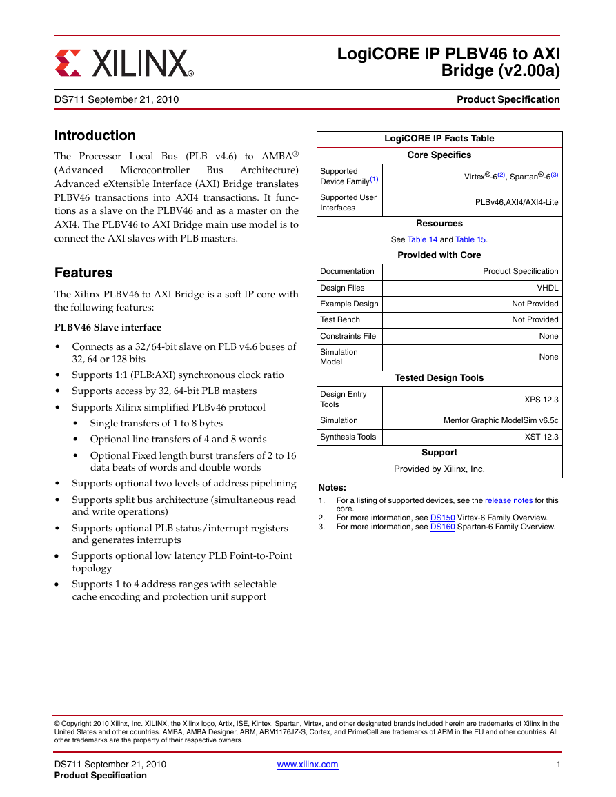
LogiCORE IP Facts Table
Core Specifics
Virtex®-6(2), Spartan®-6(3)
PLBv46,AXI4/AXI4-Lite
Resources
See Table 14 and Table 15.
Provided with Core
Product Specification
VHDL
Not Provided
Not Provided
None
None
XPS 12.3
Tested Design Tools
Mentor Graphic ModelSim v6.5c
XST 12.3
Support
Provided by Xilinx, Inc.
Notes:
1.
For a listing of supported devices, see the release notes for this
core.
For more information, see DS150 Virtex-6 Family Overview.
For more information, see DS160 Spartan-6 Family Overview.
2.
3.
© Copyright 2010 Xilinx, Inc. XILINX, the Xilinx logo, Artix, ISE, Kintex, Spartan, Virtex, and other designated brands included herein are trademarks of Xilinx in the
United States and other countries. AMBA, AMBA Designer, ARM, ARM1176JZ-S, Cortex, and PrimeCell are trademarks of ARM in the EU and other countries. All
other trademarks are the property of their respective owners.
DS711 September 21, 2010
Product Specification
www.xilinx.com
1
�
LogiCORE IP PLBV46 to AXI Bridge (v2.00a)
Features (contd)
AXI Master interface
Connects as a 32/64-bit master on 32/64-bit AXI4 interface
Connects as a 32-bit master on 32-bit AXI4-Lite interface
Supports AXI4/AXI4-Lite interfaces
Support burst transfers of 1 to 32 words or 1 to 16 double words of INCR type and burst transfers of 4 and 8
only of WRAP type
Supports optional generation of two outstanding addresses and supports out-of-order read transaction
completion and out-of-order write transaction completion
Supports optional limited cache encoding (cacheable/bufferable) and limited protection unit support
(secure/non-secure)
Functional Description
Overview
The PLBV46 to AXI Bridge translates PLB transactions into AXI transactions. The bridge functions as a slave on the
PLB and as a master on the AXI.
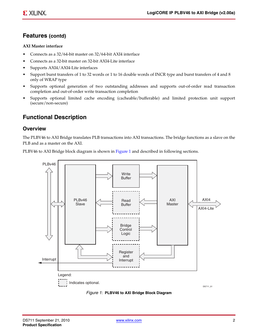
PLBV46 to AXI Bridge block diagram is shown in Figure 1 and described in following sections.
X-Ref Target - Figure 1
PLBv46
PLBv46
Slave
Write
Buffer
Read
Buffer
Bridge
Control
Logic
AXI
Master
AXI4
AXI Full/AXI Lite
AXI4-Lite
Register
and
Interrupt
Interrupt
Legend:
Indicates optional.
Figure 1: PLBV46 to AXI Bridge Block Diagram
DS711_01
DS711 September 21, 2010
Product Specification
www.xilinx.com
2
�
LogiCORE IP PLBV46 to AXI Bridge (v2.00a)
PLBv46 Slave
The PLBv46 Slave module provides a bi-directional slave interface to the PLB. The PLB data bus width can be con-
figured by setting the parameters as shown in Table 2. This module decodes the address for the bridge registers and
for the slaves on the AXI when C_SPLB_P2P = 0. This module also implements the logic to detect if overlapping
write and read requests are issued from PLB. As AXI has independent read and write channels, these requests are
issued in such a way that the data coherency is maintained.
Write Buffer
The Write Buffer stores the write data from the PLBv46 Slave module during the posted write transactions. This is
enabled when C_SPLB_SUPPORT_BURSTS = 1. The write buffer is implemented in the bridge to free up the master
transactions to other cores that may be on the PLB. The Write Buffer contains a FIFO of width 32/64-bit and depth
of 16. The width of the FIFO is directly dependent on C_SPLB_NATIVE_DWIDTH. The Write Buffer passes the
write data to the AXI Master module.
Read Buffer
The Read Buffer stores the read data from the AXI Master module during out-of-order read transactions. This is
enabled when C_M_AXI_SUPPORTS_THREADS = 1. When enabled the address pipelining depth on PLB is two
and outstanding addresses issued on AXI are two. The read buffer is needed when these back to back read transfers
on AXI are responded in out-of-order by AXI slaves. The Read Buffer contains a FIFO of width 32/64-bit and depth
of 16. The width of the FIFO is directly dependent on C_SPLB_NATIVE_DWIDTH. The Read Buffer passes the read
data to the PLBv46 Slave module.
Bridge Control Logic
The PLBV46 to AXI Bridge needs to split a burst transfer that crosses a 4K byte boundary as required by AXI. The
Bridge Control Logic module generates the 4KB crossing control signals and provides the length and address sig-
nals to the AXI Master module. This module is not used when C_SPLB_SUPPORT_BURSTS = 0 as AXI4-Lite inter-
face is used on AXI side.
Register and Interrupt
The Register and Interrupt module contains the bridge registers and generates interrupt. This is enabled when both
parameters C_EN_ERR_REGS and C_SPLB_SUPPORT_BURSTS are set to 1. These registers capture the PLB
request status and qualifiers as well as the target address when a write or read transaction generates an error on the
AXI side. Interrupt is generated to report these errors. Please refer Register Descriptions section for more details.
The register accesses are always 32-bit and only PLB single transfers are acknowledged in register address space.
The slave size is always 32-bit even when C_SPLB_NATIVE_DWIDTH is 64. This module is not implemented when
C_SPLB_SUPPORT_BURSTS = 0 and the error information is sent on Sl_MRdErr and Sl_MWrErr signals. Also the
interrupt signal is not used.
AXI Master
The AXI Master module provides a bi-directional AXI master interface on the AXI. This interface can be AXI mem-
ory-mapped interface (full AXI4) or AXI4-Lite interface (control interface) depending on the parameter
C_SPLB_SUPPORT_BURSTS. When C_SPLB_SUPPORT_BURST = 0, only single transfers on PLB will be sup-
ported and AXI4-Lite interface will be used on AXI side. When C_SPLB_SUPPORT_BURSTS = 1, AXI full interface
is used on AXI. The AXI data bus width can be 32 or 64-bits in AXI full interface and always fixed at 32 when AXI4-
Lite interface is used. This module receives read data from AXI and transmits to either read buffer when read buffer
is enabled or to PLBv46 Slave module when read buffer is disabled. During write transfers the write data is received
DS711 September 21, 2010
Product Specification
www.xilinx.com
3
�
LogiCORE IP PLBV46 to AXI Bridge (v2.00a)
from the write buffer. Depending on the design parameters, AXI Master module controls the supported limited
cache encoding (cacheable/bufferable) and limited protection encoding (secure/non-secure) signals.
I/O Signals
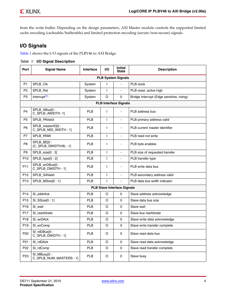
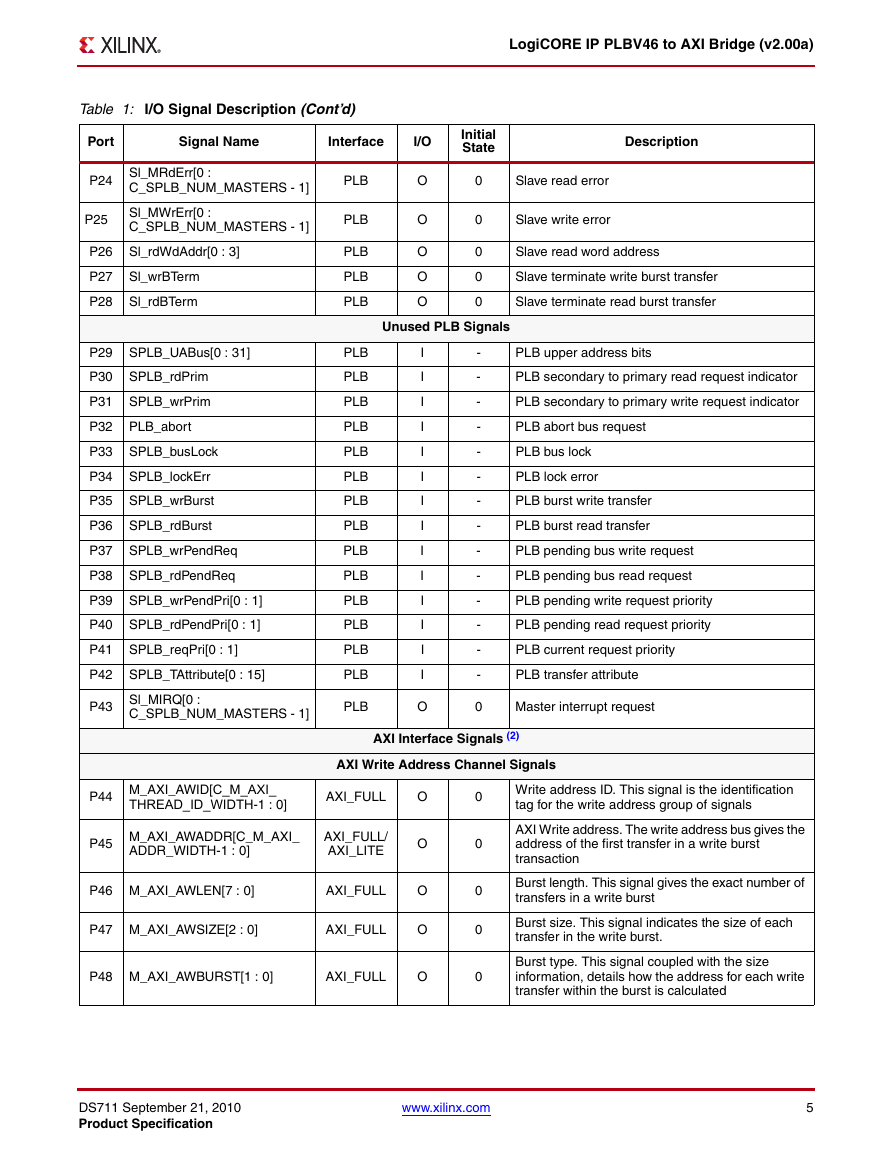
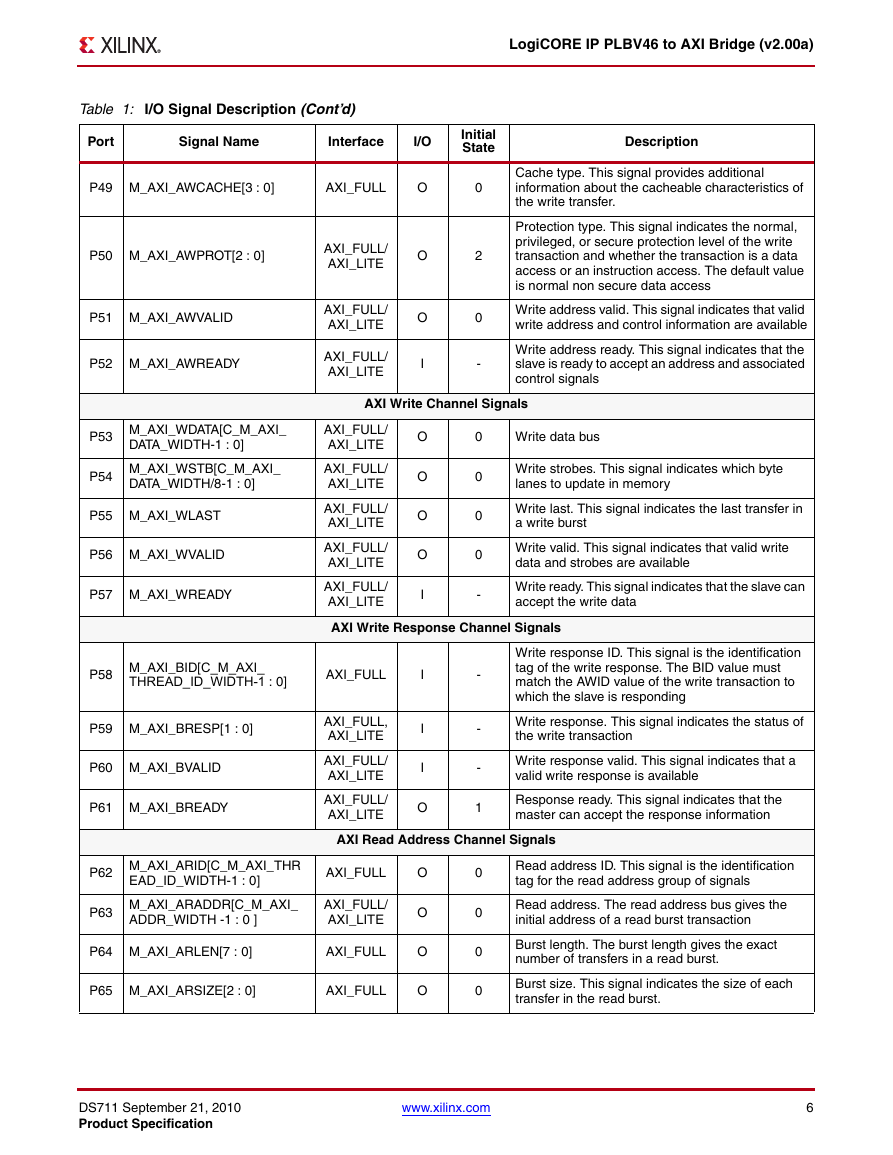
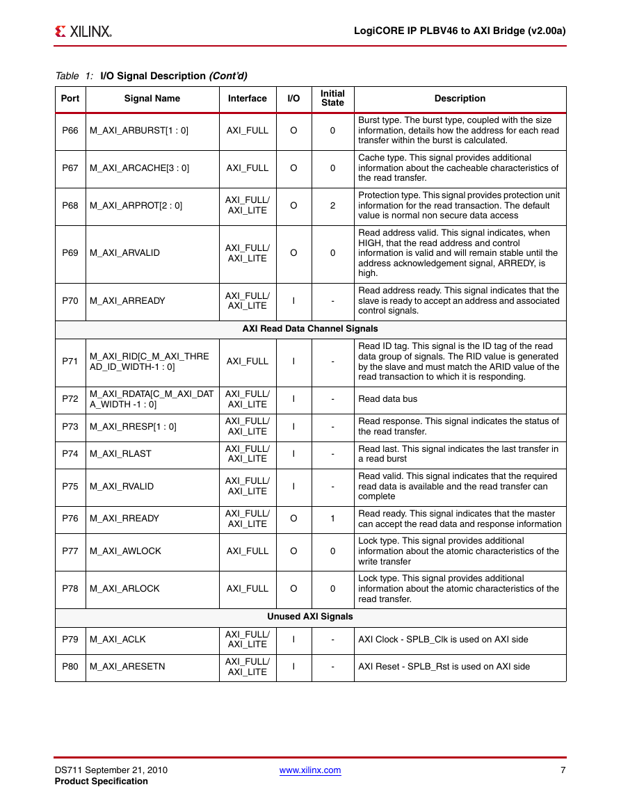
Table 1 shows the I/O signals of the PLBV46 to AXI Bridge.
Table 1: I/O Signal Description
Port
Signal Name
Interface
I/O
Initial
State
Description
P1
P2
P3
P4
P5
P6
P7
P8
P9
SPLB_Clk
SPLB_Rst
Interrupt(1)
SPLB_ABus[0 :
C_SPLB_AWIDTH -1]
SPLB_PAValid
SPLB_masterID[0 :
C_SPLB_MID_WIDTH - 1]
SPLB_RNW
SPLB_BE[0 :
(C_SPLB_DWIDTH/8) - 1]
SPLB_size[0 : 3]
P10 SPLB_type[0 : 2]
P11 SPLB_wrDBus[0 :
C_SPLB_DWIDTH - 1]
P12 SPLB_SAValid
P13 SPLB_MSize[0 : 1]
P14 Sl_addrAck
P15 Sl_SSize[0 : 1]
P16 Sl_wait
P17 Sl_rearbitrate
P18 Sl_wrDAck
P19 Sl_wrComp
P20 Sl_rdDBus[0 :
C_SPLB_DWIDTH - 1]
P21 Sl_rdDAck
P22 Sl_rdComp
P23 Sl_MBusy[0 :
C_SPLB_NUM_MASTERS - 1]
PLB System Signals
System
System
System
I
I
O
-
-
0
PLB Interface Signals
PLB clock
PLB reset, active high
Bridge Interrupt (Edge sensitive, rising)
PLB
PLB
PLB
PLB
PLB
PLB
PLB
PLB
PLB
PLB
I
I
I
I
I
I
I
I
I
I
-
-
-
-
-
-
-
-
-
-
PLB address bus
PLB primary address valid
PLB current master identifier
PLB read not write
PLB byte enables
PLB size of requested transfer
PLB transfer type
PLB write data bus
PLB secondary address valid
PLB data bus width indicator
PLB Slave Interface Signals
PLB
PLB
PLB
PLB
PLB
PLB
PLB
PLB
PLB
PLB
O
O
O
O
O
O
O
O
O
O
0
0
0
0
0
0
0
0
0
0
Slave address acknowledge
Slave data bus size
Slave wait
Slave bus rearbitrate
Slave write data acknowledge
Slave write transfer complete
Slave read data bus
Slave read data acknowledge
Slave read transfer complete
Slave busy
DS711 September 21, 2010
Product Specification
www.xilinx.com
4
�
LogiCORE IP PLBV46 to AXI Bridge (v2.00a)
Table 1: I/O Signal Description (Cont’d)
Port
Signal Name
Interface
I/O
Initial
State
Description
P24 Sl_MRdErr[0 :
C_SPLB_NUM_MASTERS - 1]
P25
Sl_MWrErr[0 :
C_SPLB_NUM_MASTERS - 1]
P26 Sl_rdWdAddr[0 : 3]
P27 Sl_wrBTerm
P28 Sl_rdBTerm
P29 SPLB_UABus[0 : 31]
P30 SPLB_rdPrim
P31 SPLB_wrPrim
P32 PLB_abort
P33 SPLB_busLock
P34 SPLB_lockErr
P35 SPLB_wrBurst
P36 SPLB_rdBurst
P37 SPLB_wrPendReq
P38 SPLB_rdPendReq
P39 SPLB_wrPendPri[0 : 1]
P40 SPLB_rdPendPri[0 : 1]
P41 SPLB_reqPri[0 : 1]
P42 SPLB_TAttribute[0 : 15]
P43 Sl_MIRQ[0 :
C_SPLB_NUM_MASTERS - 1]
PLB
PLB
PLB
PLB
PLB
PLB
PLB
PLB
PLB
PLB
PLB
PLB
PLB
PLB
PLB
PLB
PLB
PLB
PLB
PLB
O
O
O
O
O
0
0
0
0
0
Slave read error
Slave write error
Slave read word address
Slave terminate write burst transfer
Slave terminate read burst transfer
Unused PLB Signals
I
I
I
I
I
I
I
I
I
I
I
I
I
I
-
-
-
-
-
-
-
-
-
-
-
-
-
-
PLB upper address bits
PLB secondary to primary read request indicator
PLB secondary to primary write request indicator
PLB abort bus request
PLB bus lock
PLB lock error
PLB burst write transfer
PLB burst read transfer
PLB pending bus write request
PLB pending bus read request
PLB pending write request priority
PLB pending read request priority
PLB current request priority
PLB transfer attribute
O
0
Master interrupt request
AXI Interface Signals (2)
AXI Write Address Channel Signals
P44 M_AXI_AWID[C_M_AXI_
THREAD_ID_WIDTH-1 : 0]
AXI_FULL
P45 M_AXI_AWADDR[C_M_AXI_
ADDR_WIDTH-1 : 0]
AXI_FULL/
AXI_LITE
P46 M_AXI_AWLEN[7 : 0]
AXI_FULL
P47 M_AXI_AWSIZE[2 : 0]
AXI_FULL
P48 M_AXI_AWBURST[1 : 0]
AXI_FULL
O
O
O
O
O
0
0
0
0
0
Write address ID. This signal is the identification
tag for the write address group of signals
AXI Write address. The write address bus gives the
address of the first transfer in a write burst
transaction
Burst length. This signal gives the exact number of
transfers in a write burst
Burst size. This signal indicates the size of each
transfer in the write burst.
Burst type. This signal coupled with the size
information, details how the address for each write
transfer within the burst is calculated
DS711 September 21, 2010
Product Specification
www.xilinx.com
5
�
LogiCORE IP PLBV46 to AXI Bridge (v2.00a)
Table 1: I/O Signal Description (Cont’d)
Port
Signal Name
Interface
I/O
Initial
State
Description
P49 M_AXI_AWCACHE[3 : 0]
AXI_FULL
O
P50 M_AXI_AWPROT[2 : 0]
P51 M_AXI_AWVALID
P52 M_AXI_AWREADY
AXI_FULL/
AXI_LITE
AXI_FULL/
AXI_LITE
AXI_FULL/
AXI_LITE
O
O
I
0
2
0
-
Cache type. This signal provides additional
information about the cacheable characteristics of
the write transfer.
Protection type. This signal indicates the normal,
privileged, or secure protection level of the write
transaction and whether the transaction is a data
access or an instruction access. The default value
is normal non secure data access
Write address valid. This signal indicates that valid
write address and control information are available
Write address ready. This signal indicates that the
slave is ready to accept an address and associated
control signals
AXI Write Channel Signals
P53 M_AXI_WDATA[C_M_AXI_
DATA_WIDTH-1 : 0]
P54 M_AXI_WSTB[C_M_AXI_
DATA_WIDTH/8-1 : 0]
P55 M_AXI_WLAST
P56 M_AXI_WVALID
P57 M_AXI_WREADY
AXI_FULL/
AXI_LITE
AXI_FULL/
AXI_LITE
AXI_FULL/
AXI_LITE
AXI_FULL/
AXI_LITE
AXI_FULL/
AXI_LITE
O
O
O
O
I
0
0
0
0
-
Write data bus
Write strobes. This signal indicates which byte
lanes to update in memory
Write last. This signal indicates the last transfer in
a write burst
Write valid. This signal indicates that valid write
data and strobes are available
Write ready. This signal indicates that the slave can
accept the write data
AXI Write Response Channel Signals
P58 M_AXI_BID[C_M_AXI_
THREAD_ID_WIDTH-1 : 0]
P59 M_AXI_BRESP[1 : 0]
P60 M_AXI_BVALID
P61 M_AXI_BREADY
AXI_FULL
AXI_FULL,
AXI_LITE
AXI_FULL/
AXI_LITE
AXI_FULL/
AXI_LITE
I
I
I
O
Write response ID. This signal is the identification
tag of the write response. The BID value must
match the AWID value of the write transaction to
which the slave is responding
Write response. This signal indicates the status of
the write transaction
Write response valid. This signal indicates that a
valid write response is available
Response ready. This signal indicates that the
master can accept the response information
-
-
-
1
AXI Read Address Channel Signals
P62 M_AXI_ARID[C_M_AXI_THR
EAD_ID_WIDTH-1 : 0]
AXI_FULL
P63 M_AXI_ARADDR[C_M_AXI_
ADDR_WIDTH -1 : 0 ]
AXI_FULL/
AXI_LITE
P64 M_AXI_ARLEN[7 : 0]
AXI_FULL
P65 M_AXI_ARSIZE[2 : 0]
AXI_FULL
O
O
O
O
0
0
0
0
Read address ID. This signal is the identification
tag for the read address group of signals
Read address. The read address bus gives the
initial address of a read burst transaction
Burst length. The burst length gives the exact
number of transfers in a read burst.
Burst size. This signal indicates the size of each
transfer in the read burst.
DS711 September 21, 2010
Product Specification
www.xilinx.com
6
�
LogiCORE IP PLBV46 to AXI Bridge (v2.00a)
Table 1: I/O Signal Description (Cont’d)
Port
Signal Name
Interface
I/O
Initial
State
Description
P66 M_AXI_ARBURST[1 : 0]
AXI_FULL
P67 M_AXI_ARCACHE[3 : 0]
AXI_FULL
P68 M_AXI_ARPROT[2 : 0]
P69 M_AXI_ARVALID
P70 M_AXI_ARREADY
AXI_FULL/
AXI_LITE
AXI_FULL/
AXI_LITE
AXI_FULL/
AXI_LITE
O
O
O
O
I
0
0
2
0
-
Burst type. The burst type, coupled with the size
information, details how the address for each read
transfer within the burst is calculated.
Cache type. This signal provides additional
information about the cacheable characteristics of
the read transfer.
Protection type. This signal provides protection unit
information for the read transaction. The default
value is normal non secure data access
Read address valid. This signal indicates, when
HIGH, that the read address and control
information is valid and will remain stable until the
address acknowledgement signal, ARREDY, is
high.
Read address ready. This signal indicates that the
slave is ready to accept an address and associated
control signals.
AXI Read Data Channel Signals
P71 M_AXI_RID[C_M_AXI_THRE
AD_ID_WIDTH-1 : 0]
AXI_FULL
P72 M_AXI_RDATA[C_M_AXI_DAT
A_WIDTH -1 : 0]
AXI_FULL/
AXI_LITE
P73 M_AXI_RRESP[1 : 0]
P74 M_AXI_RLAST
P75 M_AXI_RVALID
P76 M_AXI_RREADY
AXI_FULL/
AXI_LITE
AXI_FULL/
AXI_LITE
AXI_FULL/
AXI_LITE
AXI_FULL/
AXI_LITE
P77 M_AXI_AWLOCK
AXI_FULL
P78 M_AXI_ARLOCK
AXI_FULL
I
I
I
I
I
O
O
O
-
-
-
-
-
1
0
0
Read ID tag. This signal is the ID tag of the read
data group of signals. The RID value is generated
by the slave and must match the ARID value of the
read transaction to which it is responding.
Read data bus
Read response. This signal indicates the status of
the read transfer.
Read last. This signal indicates the last transfer in
a read burst
Read valid. This signal indicates that the required
read data is available and the read transfer can
complete
Read ready. This signal indicates that the master
can accept the read data and response information
Lock type. This signal provides additional
information about the atomic characteristics of the
write transfer
Lock type. This signal provides additional
information about the atomic characteristics of the
read transfer.
P79 M_AXI_ACLK
P80 M_AXI_ARESETN
Unused AXI Signals
AXI_FULL/
AXI_LITE
AXI_FULL/
AXI_LITE
I
I
-
-
AXI Clock - SPLB_Clk is used on AXI side
AXI Reset - SPLB_Rst is used on AXI side
DS711 September 21, 2010
Product Specification
www.xilinx.com
7
�
LogiCORE IP PLBV46 to AXI Bridge (v2.00a)
Table 1: I/O Signal Description (Cont’d)
Port
Signal Name
Interface
I/O
Initial
State
Description
Notes:
1.
This signal is not used when C_SPLB_SUPPORT_BURSTS = 0 or C_EN_ERR_REGS = 0 as error registers are not enabled.
2. AXI_FULL interface refers to AXI Memory mapped interface (AXI Full) enabled when C_SPLB_SUPPORT_BURSTS = 1 and
AXI_LITE interface refers to AXI4-Lite interface enable when C_SPLB_SUPPORT_BURSTS = 0.
Design Parameters
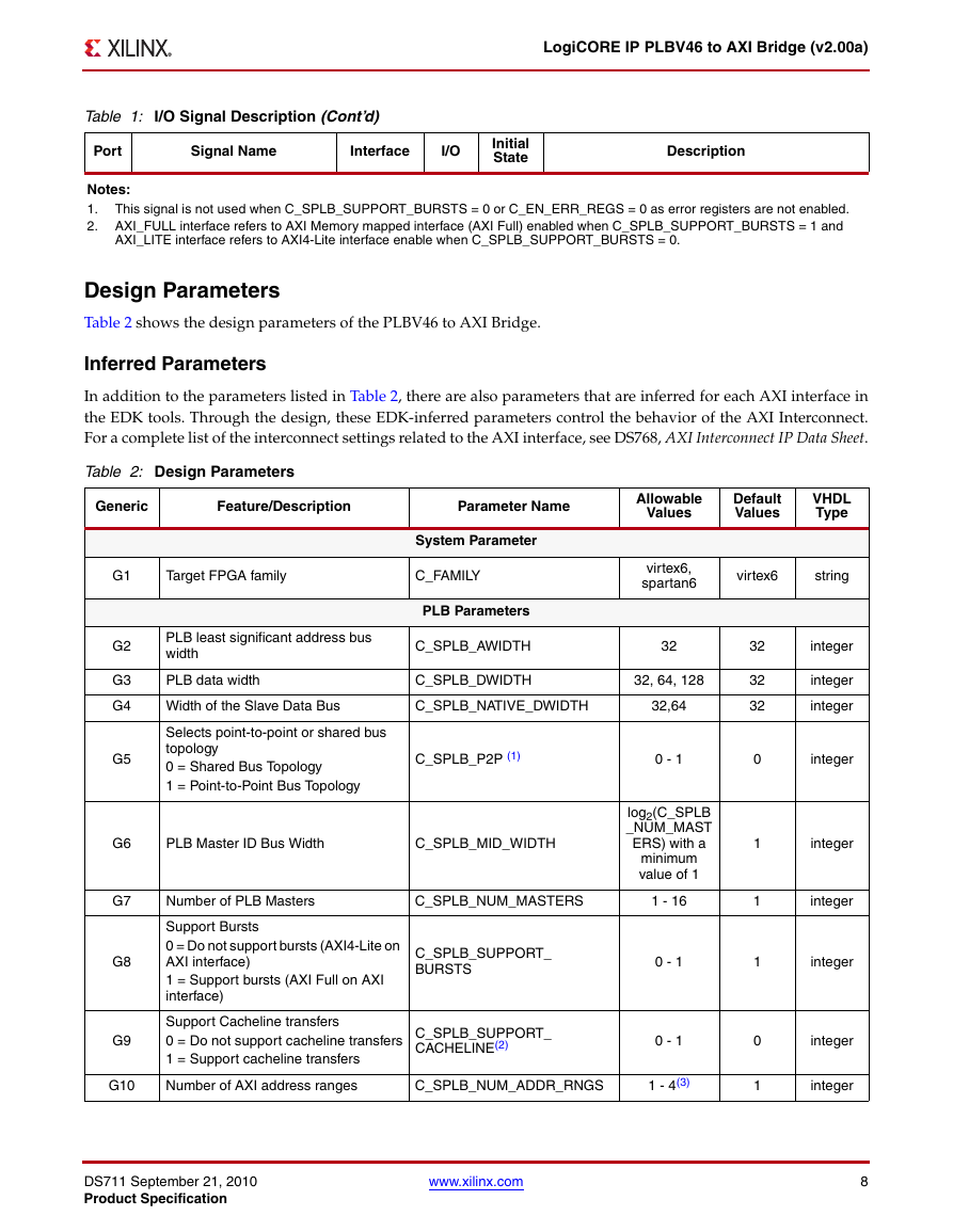
Table 2 shows the design parameters of the PLBV46 to AXI Bridge.
Inferred Parameters
In addition to the parameters listed in Table 2, there are also parameters that are inferred for each AXI interface in
the EDK tools. Through the design, these EDK-inferred parameters control the behavior of the AXI Interconnect.
For a complete list of the interconnect settings related to the AXI interface, see DS768, AXI Interconnect IP Data Sheet.
Table 2: Design Parameters
Generic
Feature/Description
Parameter Name
G1
Target FPGA family
C_FAMILY
System Parameter
Allowable
Values
Default
Values
VHDL
Type
virtex6,
spartan6
virtex6
string
G2
G3
G4
G5
PLB Parameters
PLB least significant address bus
width
C_SPLB_AWIDTH
32
PLB data width
C_SPLB_DWIDTH
32, 64, 128
Width of the Slave Data Bus
C_SPLB_NATIVE_DWIDTH
32,64
Selects point-to-point or shared bus
topology
0 = Shared Bus Topology
1 = Point-to-Point Bus Topology
C_SPLB_P2P (1)
0 - 1
G6
PLB Master ID Bus Width
C_SPLB_MID_WIDTH
log2(C_SPLB
_NUM_MAST
ERS) with a
minimum
value of 1
G7
Number of PLB Masters
C_SPLB_NUM_MASTERS
1 - 16
G8
G9
Support Bursts
0 = Do not support bursts (AXI4-Lite on
AXI interface)
1 = Support bursts (AXI Full on AXI
interface)
Support Cacheline transfers
0 = Do not support cacheline transfers
1 = Support cacheline transfers
C_SPLB_SUPPORT_
BURSTS
C_SPLB_SUPPORT_
CACHELINE(2)
G10
Number of AXI address ranges
C_SPLB_NUM_ADDR_RNGS
0 - 1
0 - 1
1 - 4(3)
32
32
32
0
1
1
1
0
1
integer
integer
integer
integer
integer
integer
integer
integer
integer
DS711 September 21, 2010
Product Specification
www.xilinx.com
8
�


 2023年江西萍乡中考道德与法治真题及答案.doc
 2012年重庆南川中考生物真题及答案.doc
 2013年江西师范大学地理学综合及文艺理论基础考研真题.doc
 2020年四川甘孜小升初语文真题及答案I卷.doc
 2020年注册岩土工程师专业基础考试真题及答案.doc
 2023-2024学年福建省厦门市九年级上学期数学月考试题及答案.doc
 2021-2022学年辽宁省沈阳市大东区九年级上学期语文期末试题及答案.doc
 2022-2023学年北京东城区初三第一学期物理期末试卷及答案.doc
 2018上半年江西教师资格初中地理学科知识与教学能力真题及答案.doc
 2012年河北国家公务员申论考试真题及答案-省级.doc
 2020-2021学年江苏省扬州市江都区邵樊片九年级上学期数学第一次质量检测试题及答案.doc
 2022下半年黑龙江教师资格证中学综合素质真题及答案.doc