ADS 2011 EM Basics (v2 October 2011)
LAB EXERCISE 2
EM Basics (Momentum)
Topics: EM simulation in ADS, focusing on Momentum, including substrate and
port setups, 3D viewing, visualization, and more.
Audience: Engineers who have a basic working knowledge of ADS 2011, have
completed the prerequisite course, or who require EM training.
Prerequisites: Completion of the course, Workspaces and Simulation Tools or
equivalent experience, including ADS layout skills.
Objectives: Be able to set up and run EM simulations from ADS layout,
including creating a substrate and defining Technology layers and materials.
© Copyright Agilent Technologies 2011
�
Table of Contents: Lab 2
1. Create a New Workspace and Layout
2. Define Dielectric Materials: Technology File
3. Draw a layout: 2 metal strips and a via
4. Open the EM Simulation Setup
5. Add a new Substrate
6. Define strip conductors (metal)
7. Add a Substrate Layer
8. Map a Via and Intruded Conductor
9.
Importing Substrates
10. EM Setup: Yellow Caution Signs
11. Selecting Pins and Defining Ports
12. Using the 3D EM Preview
13. Defining Frequency Plan, Output Plan, and Mesh Options
14. EM Model and Simulation
15. EM Simulation Data
16. Optional: Visualization of Current
Lab 2: EM Basics
3
4
5
6
6
8
9
9
11
11
12
13
14
15
16
17
Copyright 2011 Agilent Technologies
2
�
Lab 2: EM Basics
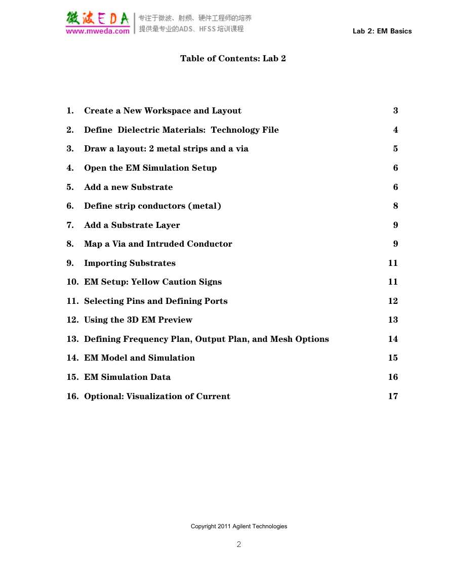
1. Create a New Workspace and Layout
a. In the ADS Main window, use the wizard to create a new workspace: File >
New > Workspace or use the icon. Name the workspace and library:
My_EM_wrk - add only the Analog/RF library as shown here and finish.
b. Create a new layout using the default cell name:
cell1, as shown here.
c. In the Layout window, select Options > Technology > Material Definitions.
When the dialog appears, select the Dielectrics tab – notice it is empty. Of
course, if you are using a PDK or library with substrates already setup, then
you might be able to see some materials listed here. This lab will show you how
to create materials for use with a substrate.
Copyright 2011 Agilent Technologies
3
�
Lab 2: EM Basics
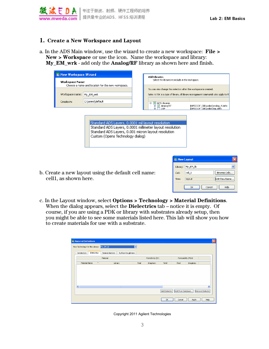
2. Define Dielectric Materials: Technology File
a. Click the Add Dielectric button and a default name (Dielectric_1) will be
added. Next, change the Real value = 6 (Permittivity) as shown here and click
Apply. You could set other values but this is enough.
b. Click the Add From
Database button and
click on Alumina from
the list of pre-defined
dielectrics. Click OK
and your two dielectrics
should appear.
Notice that you can change
the type, but leave it as
Svensson/Djordjvic.
Copyright 2011 Agilent Technologies
4
�
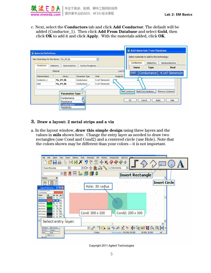
c. Next, select the Conductors tab and click Add Conductor. The default will be
added (Conductor_1). Then click Add From Database and select Gold, then
click OK to add it and click Apply. With the materials added, click OK.
Lab 2: EM Basics
3. Draw a layout: 2 metal strips and a via
a. In the layout window, draw this simple design using three layers and the
values in mils shown here. Change the entry layer as needed to draw two
rectangles (use Cond and Cond2) and a centered circle (use Hole). Note that
the colors shown may be different than your colors – it is not important.
Copyright 2011 Agilent Technologies
5
�
Lab 2: EM Basics
b. Save the layout when you have finished – you will add pins/ports later.
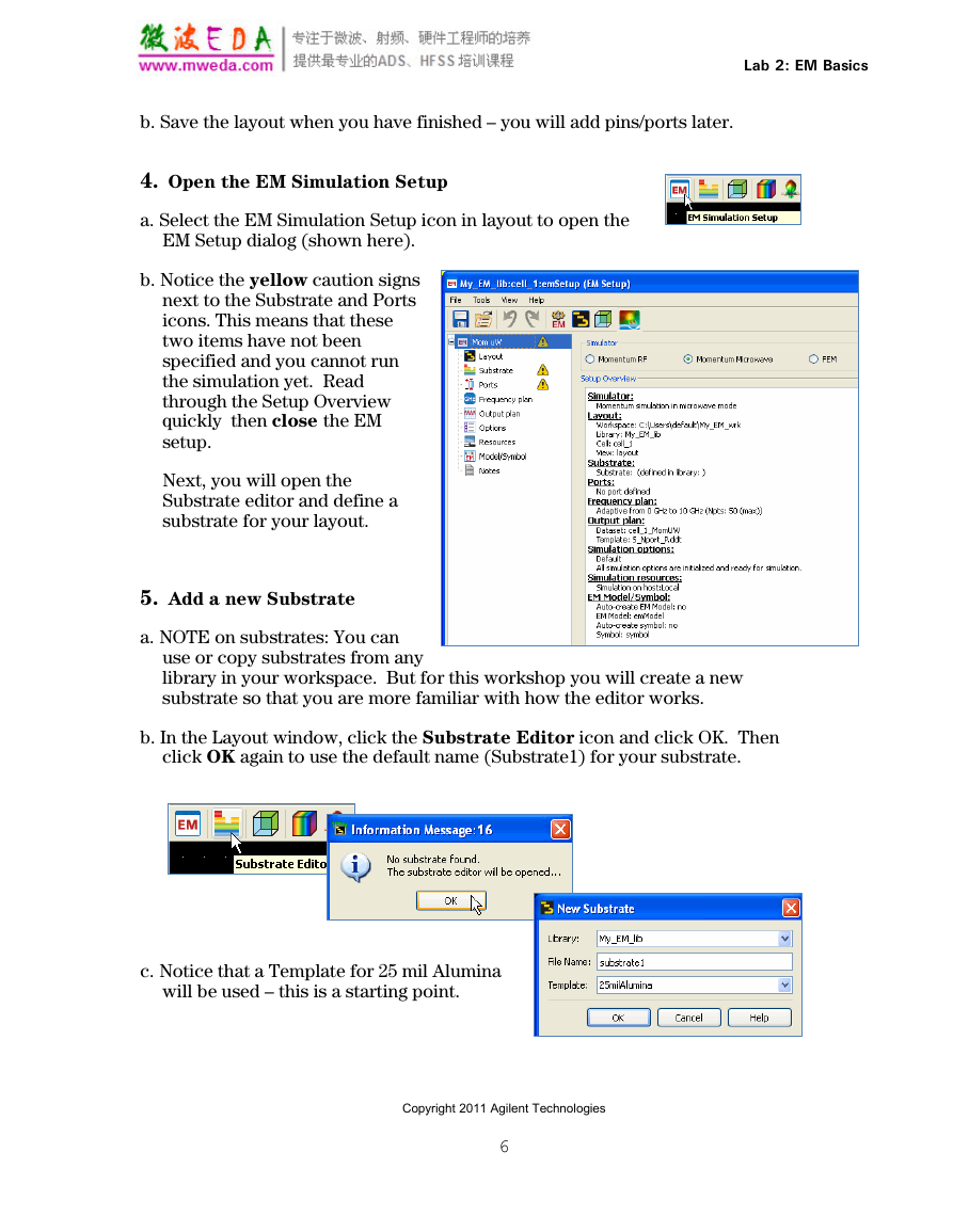
4. Open the EM Simulation Setup
a. Select the EM Simulation Setup icon in layout to open the
EM Setup dialog (shown here).
b. Notice the yellow caution signs
next to the Substrate and Ports
icons. This means that these
two items have not been
specified and you cannot run
the simulation yet. Read
through the Setup Overview
quickly then close the EM
setup.
Next, you will open the
Substrate editor and define a
substrate for your layout.
5. Add a new Substrate
a. NOTE on substrates: You can
use or copy substrates from any
library in your workspace. But for this workshop you will create a new
substrate so that you are more familiar with how the editor works.
b. In the Layout window, click the Substrate Editor icon and click OK. Then
click OK again to use the default name (Substrate1) for your substrate.
c. Notice that a Template for 25 mil Alumina
will be used – this is a starting point.
Copyright 2011 Agilent Technologies
6
�
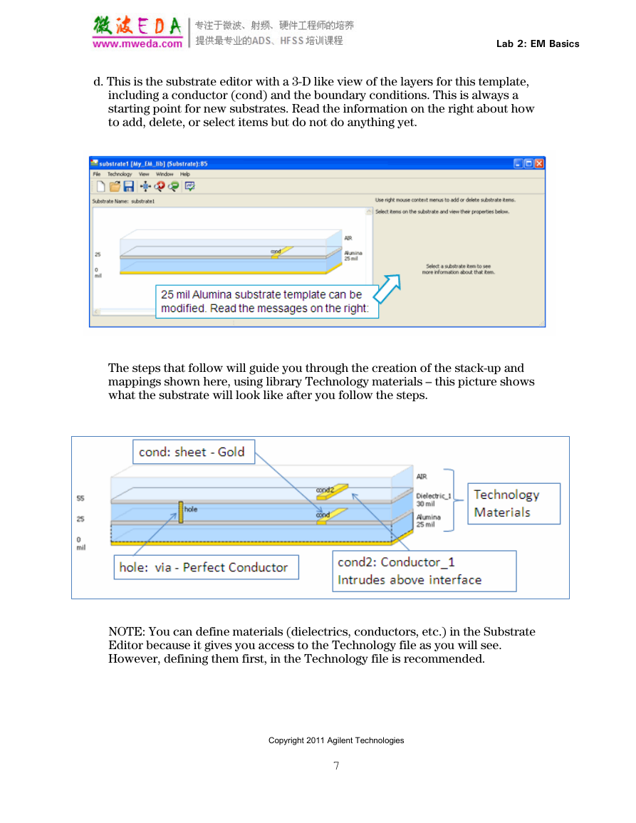
d. This is the substrate editor with a 3-D like view of the layers for this template,
including a conductor (cond) and the boundary conditions. This is always a
starting point for new substrates. Read the information on the right about how
to add, delete, or select items but do not do anything yet.
Lab 2: EM Basics
The steps that follow will guide you through the creation of the stack-up and
mappings shown here, using library Technology materials – this picture shows
what the substrate will look like after you follow the steps.
NOTE: You can define materials (dielectrics, conductors, etc.) in the Substrate
Editor because it gives you access to the Technology file as you will see.
However, defining them first, in the Technology file is recommended.
Copyright 2011 Agilent Technologies
7
�
Lab 2: EM Basics
6. Define strip conductors (metal)
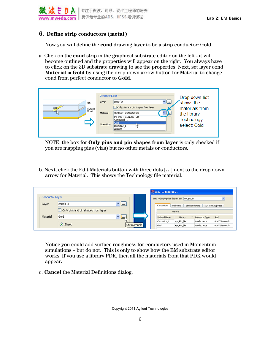
Now you will define the cond drawing layer to be a strip conductor: Gold.
a. Click on the cond strip in the graphical substrate editor on the left - it will
become outlined and the properties will appear on the right. You always have
to click on the 3D substrate drawing to see the properties. Next, set layer cond
Material = Gold by using the drop-down arrow button for Material to change
cond from perfect conductor to Gold.
NOTE: the box for Only pins and pin shapes from layer is only checked if
you are mapping pins (vias) but no other metals or conductors.
b. Next, click the Edit Materials button with three dots […] next to the drop down
arrow for Material. This shows the Technology file material.
Notice you could add surface roughness for conductors used in Momentum
simulations – but do not. This is only to show how the EM substrate editor
works. If you use a library PDK, then all the materials from that PDK would
appear.
c. Cancel the Material Definitions dialog.
Copyright 2011 Agilent Technologies
8
�


 2023年江西萍乡中考道德与法治真题及答案.doc
 2012年重庆南川中考生物真题及答案.doc
 2013年江西师范大学地理学综合及文艺理论基础考研真题.doc
 2020年四川甘孜小升初语文真题及答案I卷.doc
 2020年注册岩土工程师专业基础考试真题及答案.doc
 2023-2024学年福建省厦门市九年级上学期数学月考试题及答案.doc
 2021-2022学年辽宁省沈阳市大东区九年级上学期语文期末试题及答案.doc
 2022-2023学年北京东城区初三第一学期物理期末试卷及答案.doc
 2018上半年江西教师资格初中地理学科知识与教学能力真题及答案.doc
 2012年河北国家公务员申论考试真题及答案-省级.doc
 2020-2021学年江苏省扬州市江都区邵樊片九年级上学期数学第一次质量检测试题及答案.doc
 2022下半年黑龙江教师资格证中学综合素质真题及答案.doc