logo资料库

cpri_useguide.pdf

第1页 / 共180页
第2页 / 共180页
第3页 / 共180页
第4页 / 共180页
第5页 / 共180页
第6页 / 共180页
第7页 / 共180页
第8页 / 共180页
资料共180页,剩余部分请下载后查看
CPRI v8.7
Table of Contents
IP Facts
Ch. 1: Overview
Feature Summary
Applications
System Requirements
Recommended Design Experience
Licensing and Ordering Information
License Checkers
License Type
Ch. 2: Product Specification
Chip Period (TC) in This Document
Related Information
Performance
Maximum Frequencies
Resource Utilization
Speed Grade Support
CPRI Core Structure
Port Descriptions
Management Register Map
Status Code and Alarm Register (0x0)
Miscellaneous Status Register (0x1)
Current HDLC Rate Register (0x2)
Current Ethernet Pointer Register (0x3)
Received Subchannel 2, Word 0 Register (0x4)
Received Subchannel 2, Word 1 Register (0x5)
Received Subchannel 2, Word 2 Register (0x6)
Received Subchannel 2, Word 3 Register (0x7)
Transceiver Loopback and Ethernet Reset Request Register (0x8)
Transceiver Barrel Shift Position Register(0x9)
Preferred HDLC Rate Register (0xA)
Preferred Ethernet Pointer Register (0xB)
Current Line Speed Register (0xC)
Line Speed Capability Register (0xD)
General Configuration and Transmit CPRI Alarms Register (0xE)
R21 Timers Register (0xF)
Current Protocol Version Register (0x10)
Preferred Protocol Version Register (0x11)
Scrambler Seed Register (0x12)
Descrambler Seed Register (0x13)
Transmit FIFO Transit Time Register (0x14)
Watchdog Timeout Value Register (0x15)
Gearbox Latency Register (0x16)
FIFO Fill Level Register (0x17)
General Debug Register (0x18)
High Resolution FIFO Transit Time—Integer Part Register (0x19)
High Resolution FIFO Transit Time—Fractional Part Register (0x1A)
FEC Status Register (0x1B)
FEC CW Count Register (0x1C)
FEC Corrected CW Count Register (0x1D)
FEC Uncorrected CW Count Register (0x1E)
Ch. 3: Designing with the Core
General Design Guidelines
Use the Example Design as a Starting Point
Know the Degree of Difficulty
Keep It Registered
Recognize Timing Critical Signals
Use Supported Design Flows
Make Only Allowed Modifications
Clocking and Resets
Interfacing to the Core
Data Interfaces
I/Q Interface
UTRA-FDD I/Q Module
E-UTRA I/Q Module
Legacy Raw I/Q Module
Vendor-Specific Data Interface
Real Time Vendor-Specific Support
Frame and Synchronization Interface
HDLC Interface
Ethernet Interface
MII Interface
GMII Interface
Bandwidth Timing on the MII Interface
Connecting the CPRI core to an Ethernet MAC on the FPGA
Interface with Ethernet Frame Buffers Bypassed
ORI Module
Serial Interface
Transceiver Interface
Transceiver Debug Interface
Transceiver Data Monitor Interface
Management Interface
AXI4-Lite Memory Mapped Interface
Status and Alarm Interfaces
Static Configuration Interface
Dynamic Configuration Interface
Ch. 4: Design Considerations
Reference Clock Selection
Clock Configuration
Virtex-7, Zynq-7000, and Kintex-7 Devices
Supporting Line Rates up to 3,072.0 Mb/s
Supporting Line Rates up to 6,144.0 Mb/s
Supporting Line Rates up to 9,830.4 Mb/s
Supporting Line Rates up to 10,137.6 Mb/s
Supporting Line Rates up to 12,165.12 Mb/s
Artix-7 Devices
Supporting Line Rates up to 3,072.0 Mb/s
Supporting Line Rates up to 6,144.0 Mb/s
UltraScale Architecture Devices
Supporting Line Rates up to 3,072.0 Mb/s and 6,144 Mb/s
Supporting Line Rates up to 9,830.4 Mb/s
Supporting Line Rates up to 10,137.6 Mb/s and 12,165.12 Mb/s
Supporting Line Rates up to 24,330.24 Mb/s
UltraScale GTYE3-based Devices (368.64 MHz Reference Clock)
UltraScale GTYE3-based and UltraScale+ GTYE4-based Devices (245.76 MHz Reference Clock)
Free Running Receiver Reference Clock (Artix-7 Only)
Using the PLL to Generate the Core Clock
Resource Sharing
Transmitter Clock Sharing
Transceiver Common Block Sharing
Core Support Layer
_clocking.vhd
_tx_alignment.vhd
_gt_common.vhd
_resets.vhd
Line Speed Configuration and Negotiation
Single Speed Operation
Multi-speed Operation with Rate Negotiation
Disabling the Core
RS-FEC Enabled Mode
Using an External GMII Interface
Delay Measurement and Requirement 21 (R21)
Delay Model
Delay Through the GTXE2 Transceiver
Delay Through the GTHE2 Transceiver
Delay Through the GTPE2 Transceiver
Delay Through the GTHE3 Transceiver
Delay Through the GTYE3 Transceiver
Delay Across the CDC FIFO
Overall Delay
Core I/Q Interface
UTRA-FDD I/Q Module
R21 Calculation
Coarse Delay Measurement
Additional Pipeline Delays
Cores Supporting 3,072.0 Mb/s
Cores Supporting 4,915.2/6,144.0 Mb/s
Cores Supporting 9,830.4 Mb/s
Cores Supporting 10,137.6 Mb/s
Cores Supporting 12,165.12 Mb/s and Above
Cores supporting FEC Enabled Mode
Performing the Cable Delay Calculation
Calculating T14 (CPRI Master)
Calculating Toffset (CPRI Slave)
Calculating the Cable Delay
Example R21 Delay Calculation
R21A Calculation
R19 Calculation
Ch. 5: Design Flow Steps
Customizing and Generating the Core
Component Name
Master/Slave
Speed and Reference Clock Selection
Use 32-bit Datapath
Use 64-bit Datapath
Free Running Receive Clock
Management Clock Rate
Transceiver Settings
Transceiver Location
Reference Clock Location
GT Type
Additional Transceiver Control and Status Ports
Optional Features
Include R21 Timers
AXI4-Lite Management Interface
ORI Support
Include Ethernet Logic
Use GMII Interface
Bypass Ethernet FIFOs
Real Time Vendor-Specific Support
Line Rate Support
FEC Enabled Mode
Shared Logic
Advanced
User Parameters
Output Generation
Constraining the Core
Required Constraints
Device, Package, and Speed Grade Selections
Clock Frequencies and Clock Management
System Clock Domain
Recovered Clock Domain
Management Clock Domain
Reset Block Clock Domain
Ethernet Clock Domain
Hi-Speed Clock Domain
Clock Placement
Banking
Transceiver Placement
I/O Standard and Placement
Simulation
Synthesis and Implementation
Ch. 6: Example Design
Ch. 7: Test Bench
Appx. A: Verification, Compliance, and Interoperability
Simulation
Hardware Testing
Appx. B: Migrating and Upgrading
Migrating to the Vivado Design Suite
Upgrading in the Vivado Design Suite
Device Migration
Port Changes in Version 8.7
Port Changes in Version 8.6
Port Changes in Version 8.5
Port Changes in Version 8.4
Ports Added in Version 8.3
Ports Added in Version 8.2
Ports Added in Version 8.1
Ports Added in Version 8.0
Changed Ports in Version 8.0
Appx. C: Debugging
Finding Help on Xilinx.com
Documentation
Answer Records
Technical Support
Vivado Design Suite Debug Feature
Hardware Debug
Hardware Demonstration Design
General Checks
CPRI Specific Checks
AXI4-Lite Interface Debug
Appx. D: Additional Resources and Legal Notices
Xilinx Resources
References
Revision History
Please Read: Important Legal Notices
CPRI v8.7 LogiCORE IP Product Guide Vivado Design Suite PG056 April 5, 2017
Table of Contents IP Facts Chapter 1: Overview Feature Summary. . . . . . . . . . . . . . . . . . . . . . . . . . . . . . . . . . . . . . . . . . . . . . . . . . . . . . . . . . . . . . . . . . 5 Applications . . . . . . . . . . . . . . . . . . . . . . . . . . . . . . . . . . . . . . . . . . . . . . . . . . . . . . . . . . . . . . . . . . . . . . 6 System Requirements . . . . . . . . . . . . . . . . . . . . . . . . . . . . . . . . . . . . . . . . . . . . . . . . . . . . . . . . . . . . . . 7 Recommended Design Experience . . . . . . . . . . . . . . . . . . . . . . . . . . . . . . . . . . . . . . . . . . . . . . . . . . . . 7 Licensing and Ordering Information. . . . . . . . . . . . . . . . . . . . . . . . . . . . . . . . . . . . . . . . . . . . . . . . . . . 7 Chapter 2: Product Specification Chip Period (TC) in This Document . . . . . . . . . . . . . . . . . . . . . . . . . . . . . . . . . . . . . . . . . . . . . . . . . . . 11 Related Information. . . . . . . . . . . . . . . . . . . . . . . . . . . . . . . . . . . . . . . . . . . . . . . . . . . . . . . . . . . . . . . 11 Performance. . . . . . . . . . . . . . . . . . . . . . . . . . . . . . . . . . . . . . . . . . . . . . . . . . . . . . . . . . . . . . . . . . . . . 11 Resource Utilization. . . . . . . . . . . . . . . . . . . . . . . . . . . . . . . . . . . . . . . . . . . . . . . . . . . . . . . . . . . . . . . 12 Speed Grade Support. . . . . . . . . . . . . . . . . . . . . . . . . . . . . . . . . . . . . . . . . . . . . . . . . . . . . . . . . . . . . . 12 CPRI Core Structure . . . . . . . . . . . . . . . . . . . . . . . . . . . . . . . . . . . . . . . . . . . . . . . . . . . . . . . . . . . . . . . 13 Port Descriptions . . . . . . . . . . . . . . . . . . . . . . . . . . . . . . . . . . . . . . . . . . . . . . . . . . . . . . . . . . . . . . . . . 15 Management Register Map. . . . . . . . . . . . . . . . . . . . . . . . . . . . . . . . . . . . . . . . . . . . . . . . . . . . . . . . . 16 Chapter 3: Designing with the Core General Design Guidelines . . . . . . . . . . . . . . . . . . . . . . . . . . . . . . . . . . . . . . . . . . . . . . . . . . . . . . . . . 28 Clocking and Resets . . . . . . . . . . . . . . . . . . . . . . . . . . . . . . . . . . . . . . . . . . . . . . . . . . . . . . . . . . . . . . . 29 Interfacing to the Core. . . . . . . . . . . . . . . . . . . . . . . . . . . . . . . . . . . . . . . . . . . . . . . . . . . . . . . . . . . . . 33 Chapter 4: Design Considerations Reference Clock Selection . . . . . . . . . . . . . . . . . . . . . . . . . . . . . . . . . . . . . . . . . . . . . . . . . . . . . . . . . . 95 Clock Configuration . . . . . . . . . . . . . . . . . . . . . . . . . . . . . . . . . . . . . . . . . . . . . . . . . . . . . . . . . . . . . . . 96 Using the PLL to Generate the Core Clock . . . . . . . . . . . . . . . . . . . . . . . . . . . . . . . . . . . . . . . . . . . . 111 Resource Sharing . . . . . . . . . . . . . . . . . . . . . . . . . . . . . . . . . . . . . . . . . . . . . . . . . . . . . . . . . . . . . . . . 113 Line Speed Configuration and Negotiation . . . . . . . . . . . . . . . . . . . . . . . . . . . . . . . . . . . . . . . . . . . 121 RS-FEC Enabled Mode . . . . . . . . . . . . . . . . . . . . . . . . . . . . . . . . . . . . . . . . . . . . . . . . . . . . . . . . . . . . 122 Using an External GMII Interface . . . . . . . . . . . . . . . . . . . . . . . . . . . . . . . . . . . . . . . . . . . . . . . . . . . 122 Delay Measurement and Requirement 21 (R21) . . . . . . . . . . . . . . . . . . . . . . . . . . . . . . . . . . . . . . . 124 CPRI v8.7 PG056 April 5, 2017 www.xilinx.com 2 Send Feedback
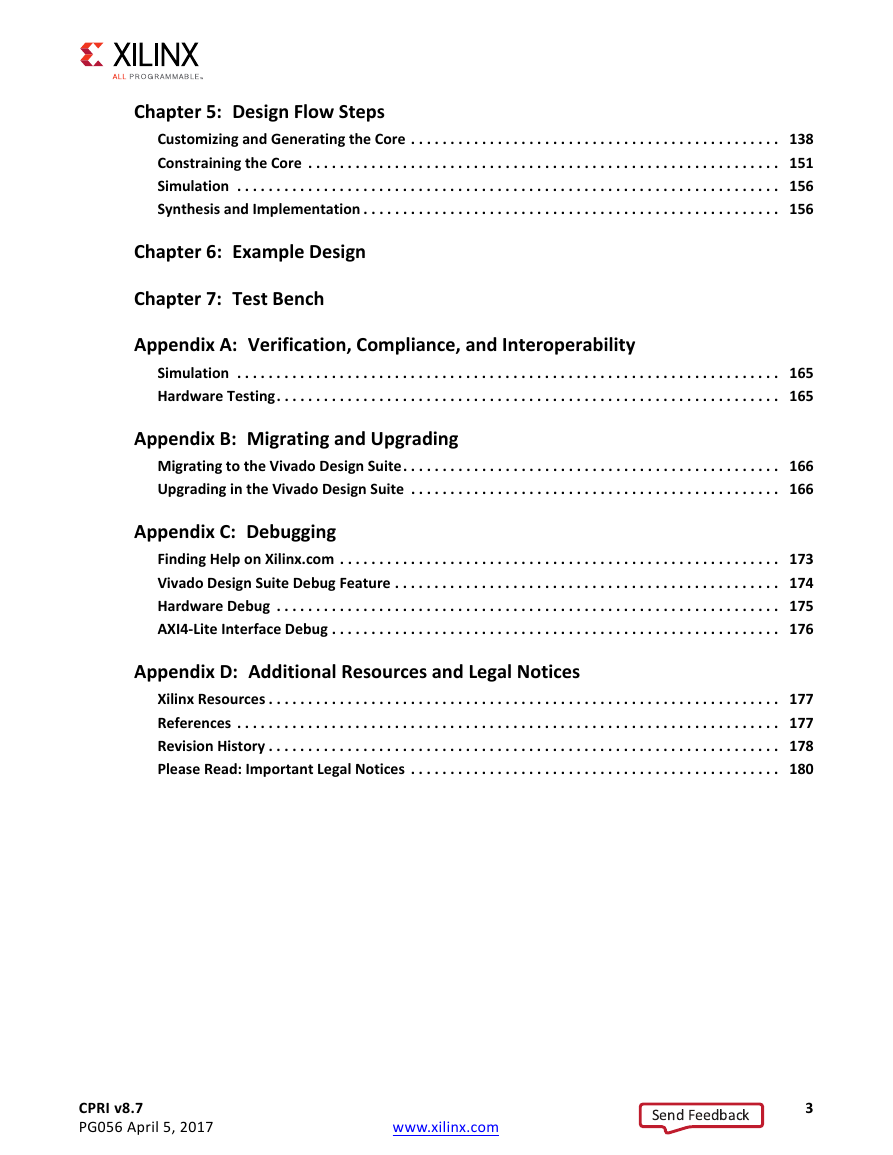
Chapter 5: Design Flow Steps Customizing and Generating the Core . . . . . . . . . . . . . . . . . . . . . . . . . . . . . . . . . . . . . . . . . . . . . . . 138 Constraining the Core . . . . . . . . . . . . . . . . . . . . . . . . . . . . . . . . . . . . . . . . . . . . . . . . . . . . . . . . . . . . 151 Simulation . . . . . . . . . . . . . . . . . . . . . . . . . . . . . . . . . . . . . . . . . . . . . . . . . . . . . . . . . . . . . . . . . . . . . 156 Synthesis and Implementation . . . . . . . . . . . . . . . . . . . . . . . . . . . . . . . . . . . . . . . . . . . . . . . . . . . . . 156 Chapter 6: Example Design Chapter 7: Test Bench Appendix A: Verification, Compliance, and Interoperability Simulation . . . . . . . . . . . . . . . . . . . . . . . . . . . . . . . . . . . . . . . . . . . . . . . . . . . . . . . . . . . . . . . . . . . . . 165 Hardware Testing. . . . . . . . . . . . . . . . . . . . . . . . . . . . . . . . . . . . . . . . . . . . . . . . . . . . . . . . . . . . . . . . 165 Appendix B: Migrating and Upgrading Migrating to the Vivado Design Suite. . . . . . . . . . . . . . . . . . . . . . . . . . . . . . . . . . . . . . . . . . . . . . . . 166 Upgrading in the Vivado Design Suite . . . . . . . . . . . . . . . . . . . . . . . . . . . . . . . . . . . . . . . . . . . . . . . 166 Appendix C: Debugging Finding Help on Xilinx.com . . . . . . . . . . . . . . . . . . . . . . . . . . . . . . . . . . . . . . . . . . . . . . . . . . . . . . . . 173 Vivado Design Suite Debug Feature . . . . . . . . . . . . . . . . . . . . . . . . . . . . . . . . . . . . . . . . . . . . . . . . . 174 Hardware Debug . . . . . . . . . . . . . . . . . . . . . . . . . . . . . . . . . . . . . . . . . . . . . . . . . . . . . . . . . . . . . . . . 175 AXI4-Lite Interface Debug . . . . . . . . . . . . . . . . . . . . . . . . . . . . . . . . . . . . . . . . . . . . . . . . . . . . . . . . . 176 Appendix D: Additional Resources and Legal Notices Xilinx Resources . . . . . . . . . . . . . . . . . . . . . . . . . . . . . . . . . . . . . . . . . . . . . . . . . . . . . . . . . . . . . . . . . 177 References . . . . . . . . . . . . . . . . . . . . . . . . . . . . . . . . . . . . . . . . . . . . . . . . . . . . . . . . . . . . . . . . . . . . . 177 Revision History . . . . . . . . . . . . . . . . . . . . . . . . . . . . . . . . . . . . . . . . . . . . . . . . . . . . . . . . . . . . . . . . . 178 Please Read: Important Legal Notices . . . . . . . . . . . . . . . . . . . . . . . . . . . . . . . . . . . . . . . . . . . . . . . 180 CPRI v8.7 PG056 April 5, 2017 www.xilinx.com 3 Send Feedback
IP Facts LogiCORE IP Facts Core Specifics Zynq® UltraScale+™ MPSoC UltraScale+ UltraScale™ Zynq-7000 All Programmable SoC(2) 7 Series(3) See Speed Grade Support. Generic data, status, configuration and management interfaces, AXI4-Lite management interface Performance and Resource Utilization web page Provided with Core Encrypted register transfer level (RTL) VHDL VHDL Xilinx Design Constraints (XDC) VHDL, Verilog N/A Tested Design Flows(4) Vivado® Design Suite For supported simulators, see the Xilinx Design Tools: Release Notes Guide. Vivado Synthesis Support Supported Device Family(1) Supported User Interfaces Resources Design Files Example Design Test Bench Constraints File Simulation Models Supported S/W Drivers Design Entry Simulation Synthesis Provided by Xilinx at the Xilinx Support web page Notes: 1. For a complete list of supported devices, see the Vivado IP catalog. 2. Excludes the Zynq-7000 010 and 020 devices. 3. Excludes the Artix-7 100T device in CSG324 and FTG256 packages. 4. For the supported version of the tool, see the Xilinx Design Tools: Release Notes Guide. Introduction The LogiCORE™ IP Common Public Radio Interface (CPRI™) core is a high-performance, low-cost flexible solution for implementation of the CPRI interface. It uses state-of-the-art transceivers to implement the Physical Layer. A compact and customizable Data Link Layer is implemented in the FPGA logic. Features • UltraScale architecture device designs operate at line rates of 614.4, 1,228.8, 2,457.6, 3,072, 4,915.2, 6,144, 8,110.08, 9,830.4, 10,137.6, 12,165.12, and 24,330.24 Mb/s using GTHE3, GTYE3, GTHE4 or GTYE4 transceivers. • Optional RS-FEC supported using GTYE3 • and GTYE4 transceivers at 24,330.24, 12,165.12, 10,137.6 and 8,110.08 Mb/s line rates. Zynq-7000, Virtex®-7, and Kintex®-7 device designs operate at line rates of 614.4, 1,228.8, 2,457.6, 3,072, 4,915.2, 6,144, 9,830.4, and 10,137.6 Mb/s using GTXE2, GTHE2 transceivers. • Artix®-7 devices designs operate at line rates of 614.4, 1,228.86 2,457.6, 3,072, 4,915.2, and 6,144 Mb/s using GTPE2 transceivers. • UTRA-FDD in-phase and quadrature-phase data (I/Q) module supporting 1 to 48 Antenna-Carriers per core • Automatic speed negotiation • Supports both Fast (Ethernet) and Slow High-Level Data Link Control (HDLC) Control and Management (C&M) channels per CPRI Specification v7.0 [Ref 1]. CPRI v8.7 PG056 April 5, 2017 www.xilinx.com 4 Product Specification Send Feedback
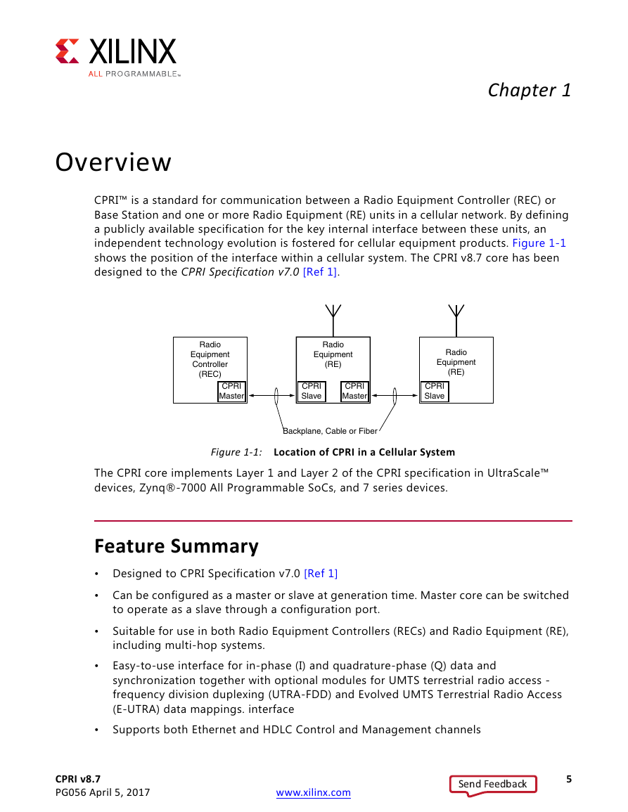
Chapter 1 Overview CPRI™ is a standard for communication between a Radio Equipment Controller (REC) or Base Station and one or more Radio Equipment (RE) units in a cellular network. By defining a publicly available specification for the key internal interface between these units, an independent technology evolution is fostered for cellular equipment products. Figure 1-1 shows the position of the interface within a cellular system. The CPRI v8.7 core has been designed to the CPRI Specification v7.0 [Ref 1]. X-Ref Target - Figure 1-1 Figure 1-1: Location of CPRI in a Cellular System The CPRI core implements Layer 1 and Layer 2 of the CPRI specification in UltraScale™ devices, Zynq®-7000 All Programmable SoCs, and 7 series devices. Feature Summary • Designed to CPRI Specification v7.0 [Ref 1] • Can be configured as a master or slave at generation time. Master core can be switched to operate as a slave through a configuration port. Suitable for use in both Radio Equipment Controllers (RECs) and Radio Equipment (RE), including multi-hop systems. Easy-to-use interface for in-phase (I) and quadrature-phase (Q) data and synchronization together with optional modules for UMTS terrestrial radio access - frequency division duplexing (UTRA-FDD) and Evolved UMTS Terrestrial Radio Access (E-UTRA) data mappings. interface Supports both Ethernet and HDLC Control and Management channels • • • CPRI v8.7 PG056 April 5, 2017 www.xilinx.com 5 Send Feedback
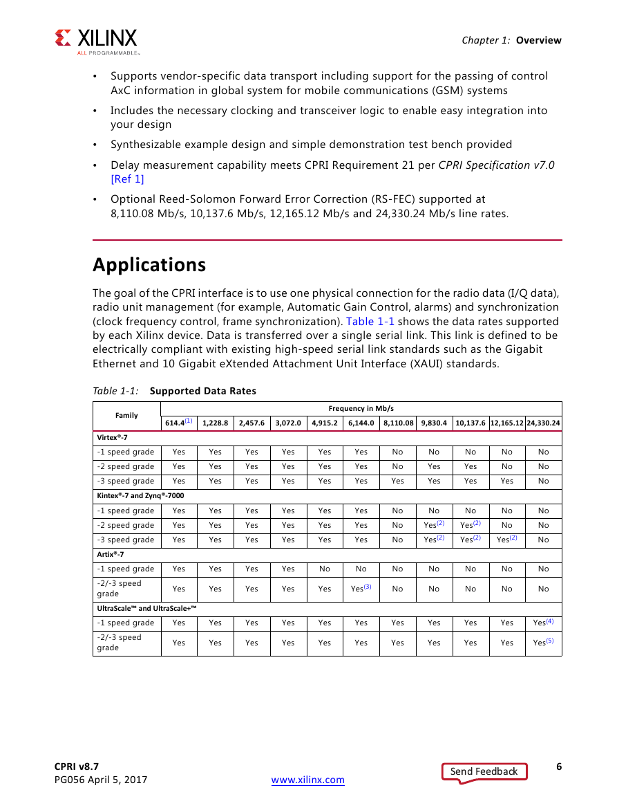
Chapter 1: Overview • • Supports vendor-specific data transport including support for the passing of control AxC information in global system for mobile communications (GSM) systems Includes the necessary clocking and transceiver logic to enable easy integration into your design Synthesizable example design and simple demonstration test bench provided • • Delay measurement capability meets CPRI Requirement 21 per CPRI Specification v7.0 [Ref 1] • Optional Reed-Solomon Forward Error Correction (RS-FEC) supported at 8,110.08 Mb/s, 10,137.6 Mb/s, 12,165.12 Mb/s and 24,330.24 Mb/s line rates. Applications The goal of the CPRI interface is to use one physical connection for the radio data (I/Q data), radio unit management (for example, Automatic Gain Control, alarms) and synchronization (clock frequency control, frame synchronization). Table 1-1 shows the data rates supported by each Xilinx device. Data is transferred over a single serial link. This link is defined to be electrically compliant with existing high-speed serial link standards such as the Gigabit Ethernet and 10 Gigabit eXtended Attachment Unit Interface (XAUI) standards. Table 1-1: Supported Data Rates Family 614.4(1) 1,228.8 2,457.6 3,072.0 4,915.2 6,144.0 8,110.08 9,830.4 10,137.6 12,165.12 24,330.24 Frequency in Mb/s Virtex®-7 Yes -1 speed grade Yes -2 speed grade Yes -3 speed grade Kintex®-7 and Zynq®-7000 Yes -1 speed grade Yes -2 speed grade -3 speed grade Yes Artix®-7 -1 speed grade -2/-3 speed grade UltraScale™ and UltraScale+™ -1 speed grade -2/-3 speed grade Yes Yes Yes Yes Yes Yes Yes Yes Yes Yes Yes Yes Yes Yes Yes Yes Yes Yes Yes Yes Yes Yes Yes Yes Yes Yes Yes Yes Yes Yes Yes Yes Yes Yes Yes Yes Yes Yes Yes Yes No Yes Yes Yes Yes Yes Yes Yes Yes Yes No Yes(3) Yes Yes No No Yes No No No No No Yes Yes No Yes Yes No Yes Yes No No Yes No Yes(2) Yes(2) No Yes(2) Yes(2) No No Yes(2) No No Yes Yes No No Yes Yes No No Yes Yes No No No No No No No No Yes(4) Yes(5) CPRI v8.7 PG056 April 5, 2017 www.xilinx.com 6 Send Feedback
Chapter 1: Overview Table 1-1: Supported Data Rates (Cont’d) Family 614.4(1) 1,228.8 2,457.6 3,072.0 4,915.2 6,144.0 8,110.08 9,830.4 10,137.6 12,165.12 24,330.24 Frequency in Mb/s Zynq UltraScale™+ MPSoC -1 speed grade Yes -2/-3 speed grade Yes Yes Yes Yes Yes Yes Yes Yes Yes Yes Yes Yes Yes Yes Yes Yes Yes Yes Yes Yes(4) Yes(5) Notes: 1. The 614.4 Mb/s line rate is not supported when the ORI option is selected. 2. Not supported on non Pb-free flip-chip BGA (FFG) packages. 3. Not supported on wire-bond packages. 4. Only supported on UltraScale+ devices using GTYE4 transceivers. 5. Only supported on UltraScale devices using GTYE3 transceivers and on UltraScale+ devices using GTYE4 transceivers. System Requirements For a list of System Requirements, see the Xilinx Design Tools: Release Notes Guide. Recommended Design Experience Although the CPRI core is a fully-verified solution, the challenge associated with implementing a complete design varies depending on the configuration and functionality of the application. For best results, previous experience building high performance, pipelined FPGA designs using Xilinx implementation software and the XDC file is recommended. Contact your local Xilinx sales representative for a closer review and estimation for your specific requirements. Licensing and Ordering Information License Checkers If the IP requires a license key, the key must be verified. The Vivado® design tools have several license check points for gating licensed IP through the flow. If the license check succeeds, the IP can continue generation. Otherwise, generation halts with error. License checkpoints are enforced by the following tools: Vivado design tools: Vivado synthesis, Vivado implementation, write_bitstream (Tcl Command). CPRI v8.7 PG056 April 5, 2017 www.xilinx.com 7 Send Feedback
Chapter 1: Overview IMPORTANT: The IP license level is ignored at checkpoints. The test confirms a valid license exists. It does not check IP license level. IMPORTANT: To use the optional 32G Fiber Channel (32GFC) RS-FEC sub-core, contact your local Xilinx sales representative to obtain your free license. License Type This Xilinx LogiCORE™ IP module is provided under the terms of the Xilinx Core License Agreement. For full access to all core functionalities in simulation and in hardware, you must purchase a license for the core. Contact your local Xilinx sales representative for information about pricing and availability of Xilinx LogiCORE IP. For more information, visit the CPRI product page. Information about this and other Xilinx LogiCORE IP modules is available at the Xilinx Intellectual Property page. For information on pricing and availability of other Xilinx LogiCORE IP modules and tools, contact your local Xilinx sales representative. CPRI v8.7 PG056 April 5, 2017 www.xilinx.com 8 Send Feedback
分享到:
收藏