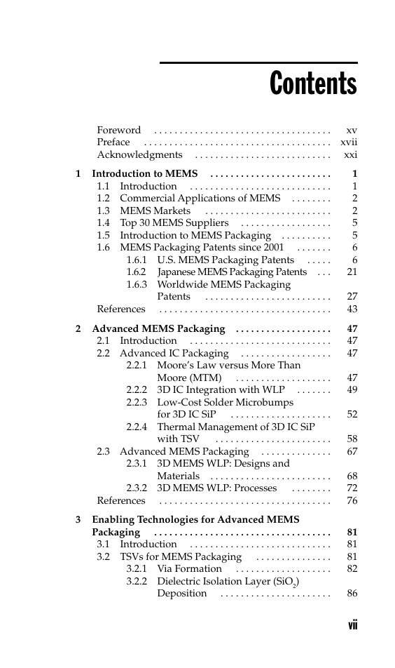
Contents
Foreword
Preface
Acknowledgments
1 Introduction to MEMS
1.1 Introduction
1.2 Commercial Applications of MEMS
1.3 MEMS Markets
1.4 Top 30 MEMS Suppliers
1.5 Introduction to MEMS Packaging
1.6 MEMS Packaging Patents since 2001
1.6.1 U.S. MEMS Packaging Patents
1.6.2 Japanese MEMS Packaging Patents
1.6.3 Worldwide MEMS Packaging Patents
References
2 Advanced MEMS Packaging
2.1 Introduction
2.2 Advanced IC Packaging
2.2.1 Moore’s Law versus More Than Moore (MTM)
2.2.2 3D IC Integration with WLP
2.2.3 Low-Cost Solder Microbumps for 3D IC SiP
2.2.4 Thermal Management of 3D IC SiP with TSV
2.3 Advanced MEMS Packaging
2.3.1 3D MEMS WLP: Designs and Materials
2.3.2 3D MEMS WLP: Processes
References
3 Enabling Technologies for Advanced MEMS Packaging
3.1 Introduction
3.2 TSVs for MEMS Packaging
3.2.1 Via Formation
3.2.2 Dielectric Isolation Layer (SiO[sub(2)]) Deposition
3.2.3 Barrier/Adhesion and Seed Metal Layer Deposition
3.2.4 Via Filling
3.2.5 Cu Polishing by Chemical/Mechanical Polish (CMP)
3.2.6 Fabrication of an ASIC Wafer with TSVs
3.2.7 Fabrication of Cap Wafer with TSVs and Cavity
3.3 Piezoresistive Stress Sensors for MEMS Packaging
3.3.1 Design and Fabrication of Piezoresistive Stress Sensors
3.3.2 Calibration of Stress Sensors
3.3.3 Stresses in Wafers after Mounting on a Dicing Tape
3.3.4 Stresses in Wafers after Thinning (Back-Grinding)
3.4 Wafer Thinning and Thin-Wafer Handling
3.4.1 3M Wafer Support System
3.4.2 EVG’s Temporary Bonding and Debonding System
3.4.3 A Simple Support-Wafer Method for Thin-Wafer Handling
3.5 Low-Temperature Bonding for MEMS Packaging
3.5.1 How Does Low-Temperature Bonding with Solders Work?
3.5.2 Low-Temperature C2C Bonding
3.5.3 Low-Temperature C2W Bonding
3.5.4 Low-Temperature W2W Bonding
3.6 MEMS Wafer Dicing
3.6.1 Fundamentals of SD Technology
3.6.2 Dicing of SOI Wafers
3.6.3 Dicing of Silicon-on-Silicon Wafers
3.6.4 Dicing of Silicon-on-Glass Wafers
3.7 RoHS-Compliant MEMS Packaging
3.7.1 EU RoHS
3.7.2 What Is the Definition of X-Free (e.g., Pb-Free)?
3.7.3 What Is a Homogeneous Material?
3.7.4 What Is the TAC?
3.7.5 How Is a Law Published in the EU RoHS Directive?
3.7.6 EU RoHS Exemptions
3.7.7 Current Status of RoHS Compliance in the Electronics Industry
3.7.8 Lead-Free Solder-Joint Reliability of MEMS Packages
References
4 Advanced MEMS Wafer-Level Packaging
4.1 Introduction
4.2 Micromachining, Wafer-Bonding Technologies, and Interconnects
4.2.1 Thin-Film Technologies
4.2.2 Bulk Micromachining Technologies
4.2.3 Conventional Wafer-Bonding Technologies for Packaging
4.2.4 Plasma-Assisted Wafer-Bonding Technologies
4.2.5 Electrical Interconnects
4.2.6 Solder-Based Intermediate-Layer Bonding
4.3 Wafer-Level Encapsulation
4.3.1 High-Temperature Encapsulation Process
4.3.2 Low-Temperature Encapsulation Process
4.4 Wafer-Level Chip Capping and MCM Technologies
4.5 Wafer-Level MEMS Packaging Based on Low-Temperature Solders: Case Study
4.5.1 Case Study: In/Ag System of Noneutectic Composition
4.5.2 Case Study: Eutectic InSn Solder for Cu-Based Metallization
4.6 Summary and Future Outlook
References
5 Optical MEMS Packaging: Communications
5.1 Introduction
5.2 Actuation Mechanisms and Integrated Micromachining Processes
5.2.1 Electrostatic Actuation
5.2.2 Thermal Actuation
5.2.3 Magnetic Actuation
5.2.4 Piezoelectric Actuation
5.2.5 Integrated Micromachining Processes
5.3 Optical Switches
5.3.1 Small-Scale Optical Switches
5.3.2 Large-Scale Optical Switches
5.4 Variable Optical Attenuators
5.4.1 Early Development Work
5.4.2 Surface-Micromachined VOAs
5.4.3 DRIE-Derived Planar VOAs Using Electrostatic Actuators
5.4.4 DRIE-Derived Planar VOAs Using Electrothermal (Thermal) Actuators
5.4.5 3D VOAs
5.4.6 VOAs Using Various Mechanisms
5.5 Packaging, Testing, and Reliability Issues
5.5.1 Manufacturability and Self-Assembly
5.5.2 Case Study: VOAs
5.5.3 Case Study: Optical Switches
5.6 Summary and Future Outlook
References
6 Optical MEMS Packaging: Bubble Switch
6.1 Introduction
6.2 3D Packaging
6.3 Boundary-Value Problem
6.3.1 Geometry
6.3.2 Materials
6.3.3 Boundary Conditions
6.4 Nonlinear Analyses of the 3D Photonic Switch
6.4.1 Creep Hysteresis Loops
6.4.2 Deflections
6.4.3 Shear-Stress Time-History
6.4.4 Shear-Creep-Strain Time-History
6.4.5 Creep-Strain Energy-Density Range
6.5 Isothermal Fatigue Tests and Results
6.5.1 Sample Preparation
6.5.2 Test Setup and Procedures
6.5.3 Test Results
6.6 Thermal Fatigue Life Prediction of the Sealing Ring
6.7 Appendix A: Package Deflection by Twyman-Green Interferometry Method
6.7.1 Sample Preparation
6.7.2 Test Setup and Procedure
6.7.3 Temperature Conditions
6.7.4 Measurement Results
6.8 Appendix B: Package Deflection by Finite-Element Method
6.9 Appendix C: Finite-Element Modeling of the Bolt
6.9.1 Description of the Bolted Model
6.9.2 Responses of the Bolted Photonic Switch
References
7 Optical MEMS: Microbolometer Packaging
7.1 Introduction
7.2 Bolometer Chip
7.3 Thermal Optimization
7.3.1 Final Temperature Stability Testing
7.4 Structural Optimization of the Package
7.5 Vacuum Packaging of Bolometer
7.5.1 Ge Window
7.6 Getter Attachment and Activation
7.7 Outgassing Study in a Vacuum Package
7.8 Testing Setup for Bolometer
7.8.1 Package Testing
7.8.2 Image Testing
References
8 Bio-MEMS Packaging
8.1 Introduction
8.2 Bio-MEMS Chip
8.3 Microfluidic Components
8.3.1 Microfluidic Cartridge
8.3.2 Biocompatible Polymeric Materials
8.4 Microfluidic Packaging
8.4.1 Polymer Microfabrication Techniques
8.4.2 Replication Technologies
8.4.3 Overview of Existing DNA and RNA Extractor Biocartridges
8.5 Fabrication of PDMS Layers
8.6 Assembly of PDMS Microfluidic Packages
8.6.1 Microfluidic Package without Reservoirs
8.6.2 Development of Reservoir and Valve
8.7 Self-Contained Microfluidic Cartridge
8.7.1 Microfluidic Package with Self-Contained Reservoirs
8.7.2 Pin-Valve Design
8.7.3 Fluid Flow-Control Mechanism
8.8 Fabrication
8.8.1 Substrate Fabrication
8.8.2 Material Selection for the Reservoir Membrane
8.9 Permeability of Material
8.10 Thermocompression Bonding
8.10.1 Bonding of PMMA to PMMA for the Channel Layer
8.10.2 Polypropylene to PMMA for Reservoir and Channel Layer
8.10.3 Tensile Test
8.11 Microfluidic Package Testing
8.11.1 Fluid Testing
8.11.2 Biologic Testing on a Biosample
8.12 Sample Preparation and Setup
8.12.1 Pretreatment of the Cartridge
8.12.2 PCR Amplification
References
9 Biosensor Packaging
9.1 Introduction
9.1.1 Review of Optical Coherence Tomography (OCT)
9.2 Biosensor Packaging
9.2.1 Micromirror
9.2.2 Single-Mode Optical Fiber and GRIN Lens
9.2.3 Upper Substrate
9.2.4 Lower Substrate
9.3 The Package
9.3.1 Configuration of the Probe
9.3.2 Optical Properties and Theories
9.3.3 Evaluations of Parameters
9.4 Optical Simulation
9.4.1 Optical Model of the Probe
9.4.2 Effect of Mirror Curvature on Coupling Efficiency
9.4.3 Effect of Lateral Tilt of a Flat Micromirror on a Curved Sample
9.4.4 Effect of Vertical Tilt of a Flat Micromirror on a Curved Sample
9.4.5 Effect of Vertical Tilt of a Flat Micromirror on a Flat Sample
9.5 Assembly of the Optical Probe
9.5.1 Fabrication of SiOB
9.5.2 Probe Assembly
9.5.3 Probe Housing
9.6 Testing of the Probe
9.6.1 Optical Alignment
9.6.2 Axial Scanning Test Result
9.6.3 Probe Imaging
9.6.4 Optical Efficiency Testing
References
10 Accelerometer Packaging
10.1 Introduction
10.2 Wafer-Level Package Requirements
10.2.1 Electrical Modeling
10.2.2 Package Structure
10.2.3 Extraction Methodology of the Interconnection Characteristics
10.3 Wafer-Level Packaging Process
10.3.1 Method 1: TSV with Sacrificial Wafer
10.3.2 Method 2: TSV without Sacrificial Wafer
10.3.3 Method 3: TSV with MEMS Wafer
10.4 Wafer Separation Process
10.4.1 Process Integration
10.5 Sacrificial Wafer Removal
10.6 Wafer-Level Vacuum Sealing
10.7 Vacuum Measurement Using a MEMS Motion Analyzer
10.8 Reliability Testing: Vacuum Maintenance
10.9 Wafer-Level 3D Package for an Accelerometer
References
11 Radiofrequency MEMS Switches
11.1 Introduction
11.2 Design of RF MEMS Switches
11.2.1 Design of Capacitive Switches
11.2.2 Design of Metal-Contact Switches
11.2.3 Mechanical Design of RF MEMS Switches
11.3 Fabrication of RF MEMS Switches
11.3.1 Surface Micromachining of RF MEMS Switches
11.3.2 Bulk Micromachining of RF MEMS Switches
11.4 Characterization of RF MEMS Switches
11.4.1 RF Performance
11.4.2 Mechanical Performance
11.5 Reliability of RF MEMS Switches
11.5.1 Reliability of Capacitive Switches
11.5.2 Reliability of Metal-Contact Switches
11.6 Summary
References
12 RF MEMS Tunable Capacitors and Tunable Band-Pass Filters
12.1 Introduction
12.2 RF MEMS Tunable Capacitors
12.2.1 Analog Tuning of RF MEMS Capacitors
12.2.2 Digital Tuning of RF MEMS Capacitors
12.3 RF MEMS Tunable Band-Pass Filters
12.3.1 Analog Tuning of a MEMS Band-Pass Filter
12.3.2 Digital Tuning of an RF MEMS Filter
12.4 Summary
References
13 Advanced Packaging of RF MEMS Devices
13.1 Introduction
13.2 Zero-Level Packaging
13.2.1 Chip Capping
13.2.2 Thin-Film Capping
13.3 One-Level Packaging
13.4 Reliability of Packaged RF MEMS Devices
13.5 Summary
References
Index
A
B
C
D
E
F
G
H
I
J
K
L
M
N
O
P
R
S
T
U
V
W
X
Y
Z





 2023年江西萍乡中考道德与法治真题及答案.doc
 2012年重庆南川中考生物真题及答案.doc
 2013年江西师范大学地理学综合及文艺理论基础考研真题.doc
 2020年四川甘孜小升初语文真题及答案I卷.doc
 2020年注册岩土工程师专业基础考试真题及答案.doc
 2023-2024学年福建省厦门市九年级上学期数学月考试题及答案.doc
 2021-2022学年辽宁省沈阳市大东区九年级上学期语文期末试题及答案.doc
 2022-2023学年北京东城区初三第一学期物理期末试卷及答案.doc
 2018上半年江西教师资格初中地理学科知识与教学能力真题及答案.doc
 2012年河北国家公务员申论考试真题及答案-省级.doc
 2020-2021学年江苏省扬州市江都区邵樊片九年级上学期数学第一次质量检测试题及答案.doc
 2022下半年黑龙江教师资格证中学综合素质真题及答案.doc