High Efficiency 1.2MHz 2A Step Up Converter 85T
High Efficiency 1.2MHz 2A Step Up Converter 85T
High Efficiency 1.2MHz 2A Step Up Converter 85T
High Efficiency 1.2MHz 2A Step Up Converter 85T
FEATURES
• Integrated 80mΩ Power MOSFET
• 2V to 24V Input Voltage
• 1.2MHz Fixed Switching Frequency
• Internal 4A Switch Current Limit
• Adjustable Output Voltage
• Internal Compensation
• Up to 28V Output Voltage
• Automatic Pulse Frequency Modulation
Mode at Light Loads
• up to 96% Efficiency
• Available in a 6-Pin SOT23-6 Package
APPLICATIONS
• Battery-Powered Equipment
• Set-Top Boxed
• LCD Bais Supply
• DSL and Cable Modems and Routers
• Networking cards powered from PCI
or PCI express slots
TYPICAL APPLICATION
includes under-voltage
GENERAL DESCRIPTION
The SX1308 is a constant frequency, 6-pin SOT23
current mode step-up converter intended for small,
low power applications. The SX1308 switches at
1.2MHz and allows the use of tiny, low cost
capacitors and inductors 2mm or less in height.
Internal soft-start results in small inrush current and
extends battery life.
The SX1308 features automatic shifting to pulse
frequency modulation mode at light loads. The
SX1308
lockout, current
limiting, and thermal overload protection to prevent
damage in the event of an output overload. The
SX1308 is available in a small 6-pin SOT-23
package.
SX1308
85T
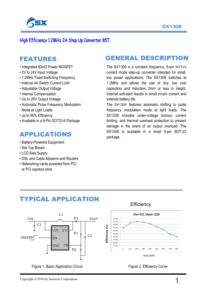
Efficiency
)
%
(
y
c
n
e
i
c
i
f
f
E
Iout (mA)
Figure 2. Efficiency Curve
Figure 1. Basic Application Circuit
Copyright ©2010 by Suosemi Corporation
1
�
SX1308
ABSOLUTE MAXIMUM RATINGS
IN, EN voltages ………..….…… -0.3V to 26V
Operating Temperature….... -40°C to +85°C
FB Voltages ................................-0.3V to 6V
Junction Temperature ………………...160°C
PACKAGE/ORDER INFORMATION
SW Voltage ……………………..-0.3V to 30V
Storage Temperature Range -65°C to 150°C
Peak SW Sink and Source Current ………4A
Lead Temperature (Soldering, 10s) ...+300°C
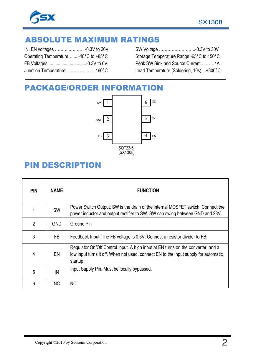
SW
GND
FB
1
2
3
6
5
4
NC
IN
EN
PIN DESCRIPTION
SOT23-6
SOT23-5
(MT3540)
(SX1308)
PIN
NAME
FUNCTION
1
2
3
4
5
6
SW
GND
Power Switch Output. SW is the drain of the internal MOSFET switch. Connect the
power inductor and output rectifier to SW. SW can swing between GND and 28V.
Ground Pin
FB
EN
IN
NC
Feedback Input. The FB voltage is 0.6V. Connect a resistor divider to FB.
Regulator On/Off Control Input. A high input at EN turns on the converter, and a
low input turns it off. When not used, connect EN to the input supply for automatic
startup.
Input Supply Pin. Must be locally bypassed.
NC
Copyright ©2010 by Suosemi Corporation
2
�
SX1308
MAX
24
1.98
1
200
2.2
0.4
0.612
150
1
unit
V
V
mV
µA
µA
mA
MHz
%
V
V
V
nA
mΩ
A
μA
℃
MIN
2
90
1.5
0.588
-50
TYP
100
0.1
100
1.6
1.2
0.6
-10
80
4
155
VEN= 0V
VFB=0.7V,No switch
VFB=0.5V,switch
VFB = 0V
VFB = 0.6V
VIN= 5V, Duty cycle=50%
VSW = 20V
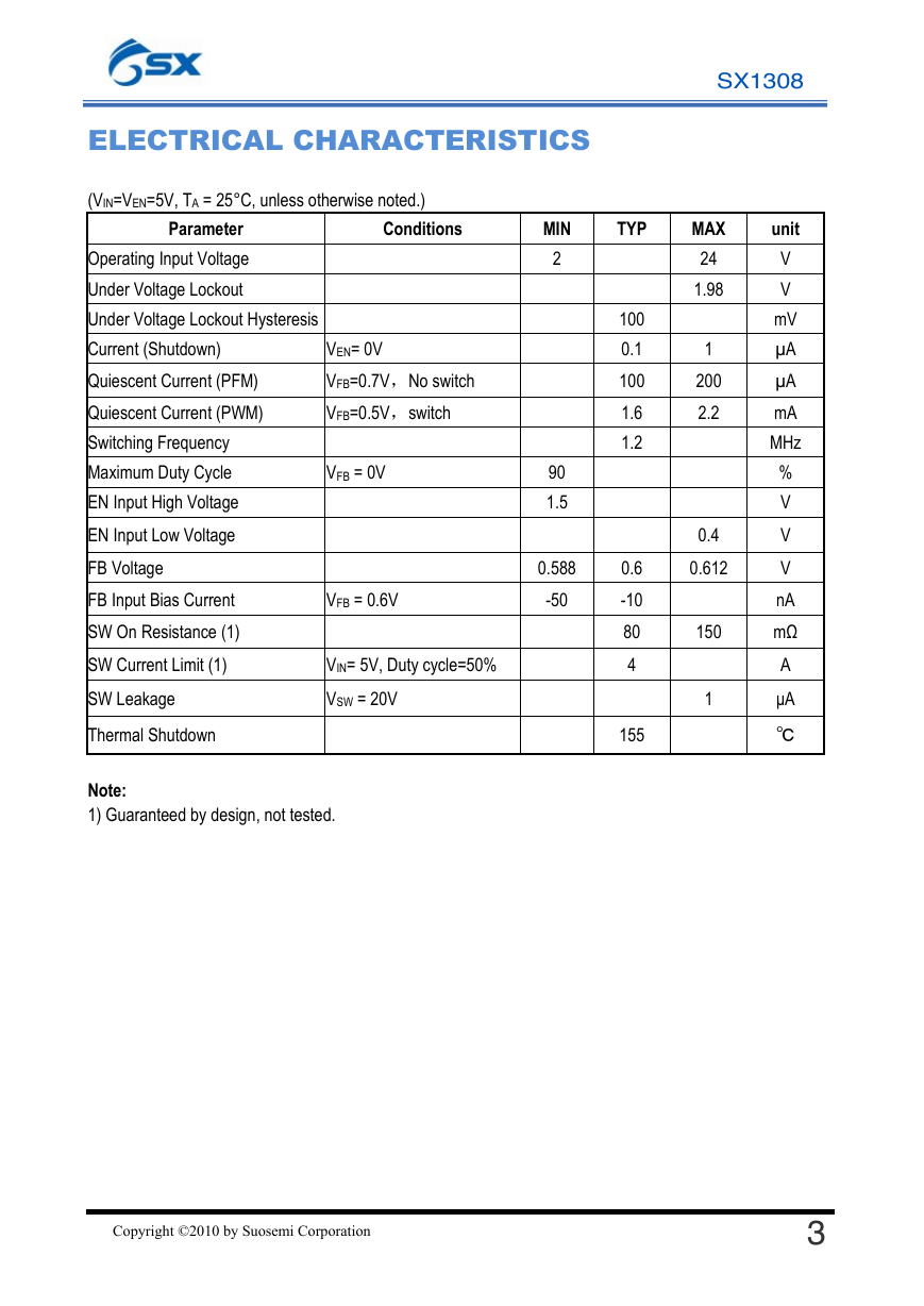
ELECTRICAL CHARACTERISTICS
(VIN=VEN=5V, TA = 25°C, unless otherwise noted.)
Conditions
Parameter
Operating Input Voltage
Under Voltage Lockout
Under Voltage Lockout Hysteresis
Current (Shutdown)
Quiescent Current (PFM)
Quiescent Current (PWM)
Switching Frequency
Maximum Duty Cycle
EN Input High Voltage
EN Input Low Voltage
FB Voltage
FB Input Bias Current
SW On Resistance (1)
SW Current Limit (1)
SW Leakage
Thermal Shutdown
Note:
1) Guaranteed by design, not tested.
Copyright ©2010 by Suosemi Corporation
3
�
to
regulator architecture
OPERATION
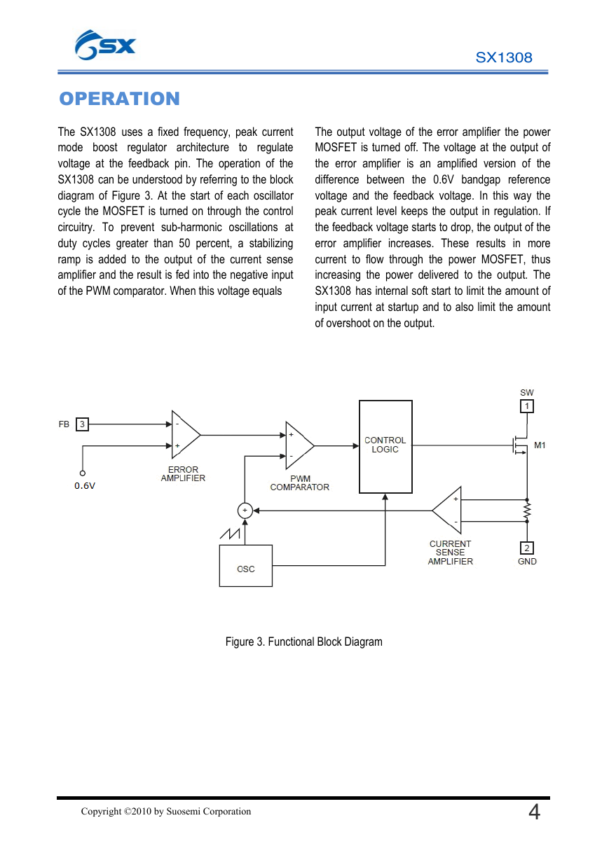
The SX1308 uses a fixed frequency, peak current
mode boost
regulate
voltage at the feedback pin. The operation of the
SX1308 can be understood by referring to the block
diagram of Figure 3. At the start of each oscillator
cycle the MOSFET is turned on through the control
circuitry. To prevent sub-harmonic oscillations at
duty cycles greater than 50 percent, a stabilizing
ramp is added to the output of the current sense
amplifier and the result is fed into the negative input
of the PWM comparator. When this voltage equals
SX1308
The output voltage of the error amplifier the power
MOSFET is turned off. The voltage at the output of
the error amplifier is an amplified version of the
difference between the 0.6V bandgap reference
voltage and the feedback voltage. In this way the
peak current level keeps the output in regulation. If
the feedback voltage starts to drop, the output of the
error amplifier increases. These results in more
current to flow through the power MOSFET, thus
increasing the power delivered to the output. The
SX1308 has internal soft start to limit the amount of
input current at startup and to also limit the amount
of overshoot on the output.
Figure 3. Functional Block Diagram
Copyright ©2010 by Suosemi Corporation
4
�
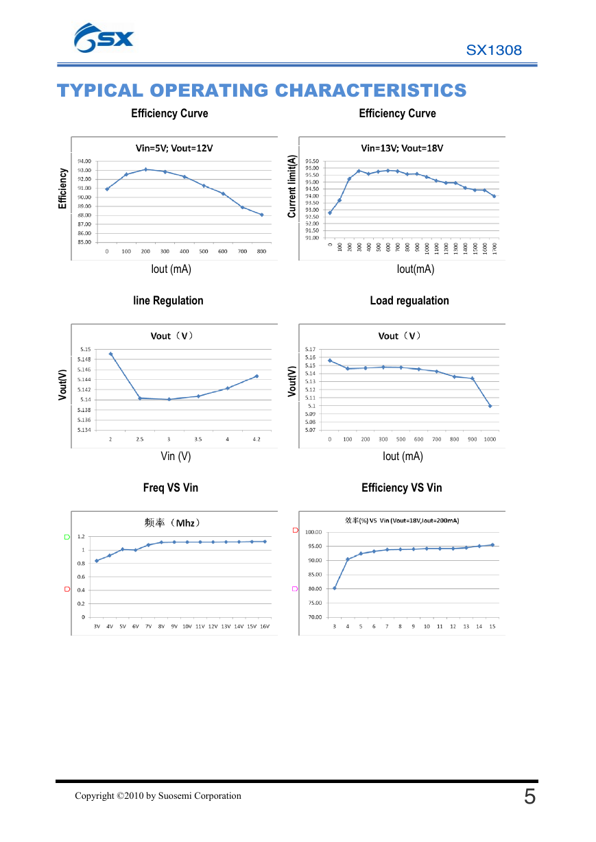
TYPICAL OPERATING CHARACTERISTICS
SX1308
y
c
n
e
c
i
f
f
i
E
)
V
(
t
u
o
V
Efficiency Curve
Iout (mA)
line Regulation
Vin (V)
Freq VS Vin
Efficiency Curve
)
A
(
t
i
m
i
l
t
n
e
r
r
u
C
Iout(mA)
Load regualation
)
V
(
t
u
o
V
Iout (mA)
Efficiency VS Vin
Copyright ©2010 by Suosemi Corporation
5
�
SX1308
APPLICATION INFORMATION
Setting the Output Voltage
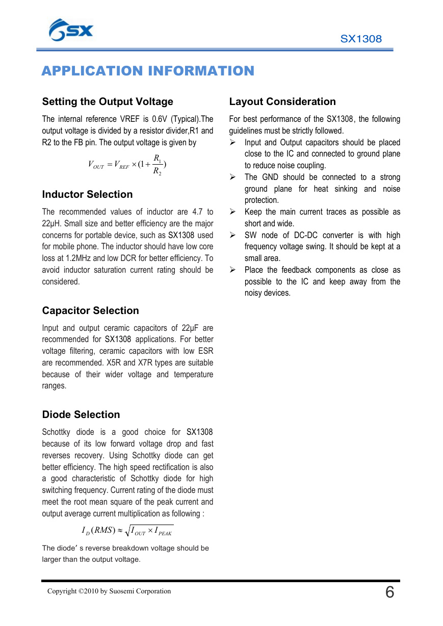
The internal reference VREF is 0.6V (Typical).The
output voltage is divided by a resistor divider,R1 and
R2 to the FB pin. The output voltage is given by
Layout Consideration
For best performance of the SX1308, the following
guidelines must be strictly followed.
V
OUT
=
V
REF
1(
+×
)
R
1
R
2
Inductor Selection
The recommended values of inductor are 4.7 to
22μH. Small size and better efficiency are the major
concerns for portable device, such as SX1308 used
for mobile phone. The inductor should have low core
loss at 1.2MHz and low DCR for better efficiency. To
avoid inductor saturation current rating should be
considered.
Capacitor Selection
Input and output ceramic capacitors of 22μF are
recommended for SX1308 applications. For better
voltage filtering, ceramic capacitors with low ESR
are recommended. X5R and X7R types are suitable
because of their wider voltage and temperature
ranges.
Diode Selection
Schottky diode
for SX1308
because of its low forward voltage drop and fast
reverses recovery. Using Schottky diode can get
better efficiency. The high speed rectification is also
a good characteristic of Schottky diode for high
switching frequency. Current rating of the diode must
meet the root mean square of the peak current and
output average current multiplication as following :
is a good choice
I
D
(
RMS
≈)
I
OUT
×
I
PEAK
The diode’ s reverse breakdown voltage should be
larger than the output voltage.
Copyright ©2010 by Suosemi Corporation
Input and Output capacitors should be placed
close to the IC and connected to ground plane
to reduce noise coupling.
The GND should be connected to a strong
for heat sinking and noise
ground plane
protection.
short and wide.
Keep the main current traces as possible as
SW node of DC-DC converter is with high
frequency voltage swing. It should be kept at a
small area.
Place the feedback components as close as
possible to the IC and keep away from the
noisy devices.
6
�
PACKAGE DESCRIPTION
TOP VIEW RECOMMENDED LAND PATTERN
FRONT VIEW SIDE VIEW
SX1308
DETAIL “A”
Figure 4. TSOT23-6/SOT23-6 Physical Dimensions
NOTE:
1)ALL DIMENSIONS ARE IN MILLIMETERS.
2) PACKAGE LENGTH DOES NOT INCLUDE MOLD FLASH,PROTRUSION OR GATE BURR.
3) PACKAGE WIDTH DOES NOT INCLUDE INTERLEAD FLASH OR PROTRUSION.
4) LEAD COPLANARITY (BOTTOM OF LEADS AFTER FORMING) SHALL BE 0.10 MILLIMETERS MAX.
5) DRAWING CONFORMS TO JEDEC MO-193, VARIATION AB.
6) DRAWING IS NOT TO SCALE.
7) PIN 1 IS LOWER LEFT PIN WHEN READING TOP MARK FROM LEFT TO RIGHT, (SEE EXAMPLE TOP MARK)
Copyright ©2010 by Suosemi Corporation
7
�


 2023年江西萍乡中考道德与法治真题及答案.doc
 2012年重庆南川中考生物真题及答案.doc
 2013年江西师范大学地理学综合及文艺理论基础考研真题.doc
 2020年四川甘孜小升初语文真题及答案I卷.doc
 2020年注册岩土工程师专业基础考试真题及答案.doc
 2023-2024学年福建省厦门市九年级上学期数学月考试题及答案.doc
 2021-2022学年辽宁省沈阳市大东区九年级上学期语文期末试题及答案.doc
 2022-2023学年北京东城区初三第一学期物理期末试卷及答案.doc
 2018上半年江西教师资格初中地理学科知识与教学能力真题及答案.doc
 2012年河北国家公务员申论考试真题及答案-省级.doc
 2020-2021学年江苏省扬州市江都区邵樊片九年级上学期数学第一次质量检测试题及答案.doc
 2022下半年黑龙江教师资格证中学综合素质真题及答案.doc